Thin double-sided package substrate and manufacture method thereof
US20080315239A1
2008-12-25
12/128,163
2008-05-28
✅ Patent granted
US 8,013,434 B2
2011-09-06
-
-
Benjamin Sandvik | Krista Soderholm
2029-12-20
Abstract:
The present invention discloses a manufacture method for a thin double-sided package substrate, which includes steps: providing a carrier; respectively forming a first conductive layer and a second conductive layer on the upper and lower surfaces of the carrier; forming a through-hole penetrating the first conductive layer and the carrier but not penetrating the second conductive layer; setting a conductive element in the through-hole to electrically connect the first conductive layer with the second conductive layer; forming desired circuits on the first conductive layer and/or the second conductive layer; forming a first metal layer on the first conductive layer and/or the second conductive layer; and removing the carrier located in a predetermined region to form a chip receiving bay. The present invention also discloses a package substrate made by the abovementioned manufacture method, which can reduce the overall thickness of a chip package structure, increase the heat-dissipation effect of the chip and prevent the chip package structure from humidity penetration.
Inventors:
- Hung Jen Wang 7 🇹🇼 Gueishan Township, Taiwan
- Jen Feng Tseng 5 🇹🇼 Jhongli City, Taiwan
- Chi Chih Lin 3 🇹🇼 Pingihen City, Taiwan
- Bo Sun 3 🇹🇼 Pingihen City, Taiwan
- Chi Chih Lin 1 🇹🇼 Pingihen, Taiwan
- Bo Sun 1 🇹🇼 Pingihen, Taiwan
- Jen Feng Tseng 1 🇹🇼 Jhongli, Taiwan
Assignee:
- Taiwan Solutions System Corp. 1 🇹🇼 Hsinchu City, Taiwan
- Light Ocean Technology Corp. 2 🇹🇼 Taoyuan County, Taiwan
Interested in similar patents?
Get notified when new applications in this technology area are published.
Classification:
H01L23/3735 » CPC main
Details of semiconductor or other solid state devices; Arrangements for cooling, heating, ventilating or temperature compensation ; Temperature sensing arrangements; Selection of materials, or shaping, to facilitate cooling or heating, e.g. heatsinks; Cooling facilitated by selection of materials for the device or materials for thermal expansion adaptation, e.g. carbon Laminates or multilayers, e.g. direct bond copper ceramic substrates
H01L21/486 » CPC further
Processes or apparatus adapted for the manufacture or treatment of semiconductor or solid state devices or of parts thereof; Manufacture or treatment of semiconductor devices or of parts thereof the devices having at least one potential-jump barrier or surface barrier, e.g. PN junction, depletion layer or carrier concentration layer; Manufacture or treatment of parts, e.g. containers, prior to assembly of the devices, using processes not provided for in a single one of the subgroups -; Conductive parts; Leads on or in insulating or insulated substrates, e.g. metallisation Via connections through the substrate with or without pins
H01L23/13 » CPC further
Details of semiconductor or other solid state devices; Mountings, e.g. non-detachable insulating substrates characterised by the shape
H01L23/49822 » CPC further
Details of semiconductor or other solid state devices; Arrangements for conducting electric current to or from the solid state body in operation, e.g. leads, terminal arrangements ; Selection of materials therefor consisting of soldered constructions; Leads, on insulating substrates, Multilayer substrates
H01L23/49827 » CPC further
Details of semiconductor or other solid state devices; Arrangements for conducting electric current to or from the solid state body in operation, e.g. leads, terminal arrangements ; Selection of materials therefor consisting of soldered constructions; Leads, on insulating substrates, Via connections through the substrates, e.g. pins going through the substrate, coaxial cables
H01L33/486 » CPC further
Semiconductor devices with at least one potential-jump barrier or surface barrier specially adapted for light emission; Processes or apparatus specially adapted for the manufacture or treatment thereof or of parts thereof; Details thereof characterised by the semiconductor body packages; Containers adapted for surface mounting
H01L24/48 » CPC further
Arrangements for connecting or disconnecting semiconductor or solid-state bodies; Methods or apparatus related thereto; Means for bonding being attached to, or being formed on, the surface to be connected, e.g. chip-to-package, die-attach, "first-level" interconnects; Manufacturing methods related thereto; Wire connectors; Manufacturing methods related thereto; Structure, shape, material or disposition of the wire connectors after the connecting process of an individual wire connector
H01L24/73 » CPC further
Arrangements for connecting or disconnecting semiconductor or solid-state bodies; Methods or apparatus related thereto Means for bonding being of different types provided for in two or more of groups , , , , , , ,
H01L24/83 » CPC further
Arrangements for connecting or disconnecting semiconductor or solid-state bodies; Methods or apparatus related thereto; Methods for connecting semiconductor or other solid state bodies using means for bonding being attached to, or being formed on, the surface to be connected using a layer connector
H01L24/85 » CPC further
Arrangements for connecting or disconnecting semiconductor or solid-state bodies; Methods or apparatus related thereto; Methods for connecting semiconductor or other solid state bodies using means for bonding being attached to, or being formed on, the surface to be connected using a wire connector
H01L33/60 » CPC further
Semiconductor devices with at least one potential-jump barrier or surface barrier specially adapted for light emission; Processes or apparatus specially adapted for the manufacture or treatment thereof or of parts thereof; Details thereof characterised by the semiconductor body packages; Optical field-shaping elements Reflective elements
H01L2224/83801 » CPC further
Indexing scheme for arrangements for connecting or disconnecting semiconductor or solid-state bodies and methods related thereto as covered by; Methods for connecting semiconductor or other solid state bodies using means for bonding being attached to, or being formed on, the surface to be connected using a layer connector; Bonding techniques Soldering or alloying
H01L2224/85 » CPC further
Indexing scheme for arrangements for connecting or disconnecting semiconductor or solid-state bodies and methods related thereto as covered by; Methods for connecting semiconductor or other solid state bodies using means for bonding being attached to, or being formed on, the surface to be connected using a wire connector
H01L2924/01046 » CPC further
Indexing scheme for arrangements or methods for connecting or disconnecting semiconductor or solid-state bodies as covered by; Chemical elements Palladium [Pd]
H01L2924/01078 » CPC further
Indexing scheme for arrangements or methods for connecting or disconnecting semiconductor or solid-state bodies as covered by; Chemical elements Platinum [Pt]
H01L2924/01079 » CPC further
Indexing scheme for arrangements or methods for connecting or disconnecting semiconductor or solid-state bodies as covered by; Chemical elements Gold [Au]
H01L2924/15153 » CPC further
Indexing scheme for arrangements or methods for connecting or disconnecting semiconductor or solid-state bodies as covered by; Details of package parts other than the semiconductor or other solid state devices to be connected; Die mounting substrate; Shape the die mounting substrate comprising a recess for hosting the device
H01L2924/15165 » CPC further
Indexing scheme for arrangements or methods for connecting or disconnecting semiconductor or solid-state bodies as covered by; Details of package parts other than the semiconductor or other solid state devices to be connected; Die mounting substrate Monolayer substrate
H01L2924/1517 » CPC further
Indexing scheme for arrangements or methods for connecting or disconnecting semiconductor or solid-state bodies as covered by; Details of package parts other than the semiconductor or other solid state devices to be connected; Die mounting substrate Multilayer substrate
Y10T29/49165 » CPC further
Metal working; Method of mechanical manufacture; Electrical device making; Conductor or circuit manufacturing; On flat or curved insulated base, e.g., printed circuit, etc.; Manufacturing circuit on or in base by forming conductive walled aperture in base
H01L2224/73265 » CPC further
Indexing scheme for arrangements for connecting or disconnecting semiconductor or solid-state bodies and methods related thereto as covered by; Means for bonding being of different types provided for in two or more of groups; Location after the connecting process on different surfaces Layer and wire connectors
H01L2924/00011 » CPC further
Indexing scheme for arrangements or methods for connecting or disconnecting semiconductor or solid-state bodies as covered by; Technical content checked by a classifier Not relevant to the scope of the group, the symbol of which is combined with the symbol of this group
H01L2224/83851 » CPC further
Indexing scheme for arrangements for connecting or disconnecting semiconductor or solid-state bodies and methods related thereto as covered by; Methods for connecting semiconductor or other solid state bodies using means for bonding being attached to, or being formed on, the surface to be connected using a layer connector; Bonding techniques using a polymer adhesive, e.g. an adhesive based on silicone, epoxy, polyimide, polyester being an anisotropic conductive adhesive
H01L2924/12041 » CPC further
Indexing scheme for arrangements or methods for connecting or disconnecting semiconductor or solid-state bodies as covered by; Details of semiconductor or other solid state devices to be connected; Device type; Passive devices, e.g. 2 terminal devices; Optical Diode LED
H01L2924/00 » CPC further
Indexing scheme for arrangements or methods for connecting or disconnecting semiconductor or solid-state bodies as covered by
H01L2924/181 » CPC further
Indexing scheme for arrangements or methods for connecting or disconnecting semiconductor or solid-state bodies as covered by; Details of package parts other than the semiconductor or other solid state devices to be connected Encapsulation
H01L2924/00012 » CPC further
Indexing scheme for arrangements or methods for connecting or disconnecting semiconductor or solid-state bodies as covered by; Technical content checked by a classifier Relevant to the scope of the group, the symbol of which is combined with the symbol of this group
H01L2224/45099 » CPC further
Indexing scheme for arrangements for connecting or disconnecting semiconductor or solid-state bodies and methods related thereto as covered by; Means for bonding being attached to, or being formed on, the surface to be connected, e.g. chip-to-package, die-attach, "first-level" interconnects; Manufacturing methods related thereto; Wire connectors; Manufacturing methods related thereto; Structure, shape, material or disposition of the wire connectors prior to the connecting process of an individual wire connector; Core members of the connector Material
H01L2924/00014 » CPC further
Indexing scheme for arrangements or methods for connecting or disconnecting semiconductor or solid-state bodies as covered by; Technical content checked by a classifier the subject-matter covered by the group, the symbol of which is combined with the symbol of this group, being disclosed without further technical details
H01L2924/207 » CPC further
Indexing scheme for arrangements or methods for connecting or disconnecting semiconductor or solid-state bodies as covered by; Parameters Diameter ranges
H01L23/48 IPC
Details of semiconductor or other solid state devices Arrangements for conducting electric current to or from the solid state body in operation, e.g. leads, terminal arrangements ; Selection of materials therefor
H05K3/42 IPC
Apparatus or processes for manufacturing printed circuits; Forming printed elements for providing electric connections to or between printed circuits Plated through-holes or plated via connections
H05K3/42 IPC
Apparatus or processes for manufacturing printed circuits; Forming printed elements for providing electric connections to or between printed circuits Plated through-holes or plated via connections
H01L33/00 IPC
Semiconductor devices with at least one potential-jump barrier or surface barrier specially adapted for light emission; Processes or apparatus specially adapted for the manufacture or treatment thereof or of parts thereof; Details thereof
Description
BACKGROUND OF THE INVENTION
1. Field of the Invention
The present invention relates to a package substrate and a manufacture method thereof, particularly to a thin double-sided package substrate and a manufacture method thereof
2. Description of the Related Art
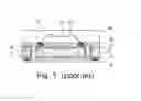
Refer to FIG. 1 In a conventional package substrate having circuits on both sides thereof, conductive layers 11 and 12 are respectively formed on the upper and lower surfaces of a carrier 11, and the desired circuits are formed on the conductive layers 11 and 12. A through-hole 14 penetrates the carrier 11, and a conductive element 15 is set inside the through-hole 14 to electrically connect the conductive layer 12 with the conductive layer 13. Besides, an insulating material, such as a resin or a solder mask, may further be filled into the through-hole 14. A metal finishing process is used to form a solder pad 17. A solder mask layer 16 is formed oil the conductive layers 12 and 13 with the solder pad 17 exposed.
As shown in FIG. 1, a chip 21 is fixedly installed on the package substrate, and wires 22 electrically connect the chip 21 with package substrate. Then, an encapsulant 23 is used to encapsulate the chip 21, the wires 22, etc., to complete the package of a chip. However, the abovementioned package structure has the following disadvantages: 1. The solder mask layer 16, the conductive layers 12 and 13, and carrier 11 are likely to peel off because of the poor bonding therebetween; 2. Humidity is likely to permeate from the non-encapsulated lower surface of the carrier 11 through the inner wall of the through-hole 14 to the upper surface of the carrier 11 because the through-hole 14 penetrates the carrier 11 and the conductive layers 12 and 13, and the reliability of the circuit is thus reduced. Besides, the chip 21 is fixedly installed on the package substrate which not only makes worse the heat dissipation of the chip 21 but also impairs the slimming of the chip package.
Therefore, how to promote reliability, reduce thickness, enhance heat dissipation and increase layout flexibility in a chip package has become an important topic in the fields concerned.
SUMMARY OF THE INVENTION
One objective of the present invention is to provide a thin double-sided package substrate and a manufacture method thereof to overcome the abovementioned problems, wherein the carrier is partially or totally removed to form a chip receiving bay accommodating a chip so as to reduce the package thickness and enhance the heat dissipation of the chip, and wherein the through-hole does not penetrate the lower conductive layer lest humidity permeate through the inner wall of the through-hole to the upper surface of the carrier, whereby the reliability of the chip package is promoted and the flexibility of the circuit layout is increased.
To achieve the abovementioned objective, one embodiment of the present invention proposes a thin double-sided package substrate, which includes: a carrier, at least one first conductive layer, at least one second conductive layer, a conductive element, a first metal layer and at least one chip receiving bay. The carrier has a first surface, a second surface and a through-hole, and the through-hole penetrates the first and second surfaces. The first conductive layer is formed on the first surface, and the second conductive layer is formed on the second surface, wherein the second conductive layer covers one opening of the through-hole. The conductive element is set in the through-hole and electrically connects the first conductive layer with the second conductive layer. The first metal layer is formed on the first conductive layer and/or the second conductive layer. The chip receiving bay is arranged in the carrier and accommodates at least one chip.
To achieve the abovementioned objective one embodiment of the present invention proposes a manufacture method for a thin double-sided package substrate. Which includes: providing a carrier having, a first surface and a second surface; forming a first conductive layer on the first surface; forming a second conductive layer on the second surface; forming a through-hole penetrating the first conductive layer and the carrier but not penetrating the second conductive layer; setting in the through-hole a conductive element electrically connecting the first conductive layer with the second conductive layer; forming desired circuits in the first conductive layer and/or the second conductive layer; forming a first metal layer in the first conductive layer and/or the second conductive layer; and removing a portion of the carrier in a predetermined region to form a chip receiving bay for accommodating at least one chip.
Below, the embodiments are described in detail in cooperation with the attached drawings to make easily understood the objectives, technical contents, characteristics and accomplishments of the present invention.
BRIEF DESCRIPTION OF THE DRAWINGS
FIG. 1 is a sectional view schematically showing a chip package structure using a conventional package substrate;
FIGS. 2a-2f are sectional views schematically showing the process of a manufacture method for a thin double-sided package substrate according to a preferred embodiment of the present invention:
FIGS. 3a-3c are sectional views schematically showing that the chip package structures using the thin double-sided package substrates according to embodiments of the present invention; and
FIGS. 4a-4c are sectional views schematically showing the chip package structures using the thin double-sided package substrates according to other embodiments of the present invention.
DETAILED DESCRIPTION OF THE INVENTION
Refer to from FIG. 2a to FIG. 2f for illustrating the process of a manufacture method for a thin double-sided package substrate according to a preferred embodiment of the present invention. Refer to FIG. 2a. Firstly, a carrier 31 having a first surface 311 and a second surface 312 is provided. The carrier 31 may be made of a copper clad laminate, an insulating material, a glass fiber prepreg, or a polymeric material etc. A first conductive layer 32 and a second conductive layer 33 are respectively formed on the first surface 311 and the second surface 312. The first and second conductive layers 32 and 33 may be made of a metal, preferably copper.
Refer to FIG. 2b. A through-hole 34 penetrates the first conductive layer 32, the first and second surfaces 311 and 312 of the carrier 31. It is to be noted that the through-hole 34 does not penetrate the second conductive layer 33. Therefore, humidity will not permeate through the inner wall of the through-hole 34 to the upper layer of the carrier 31 but will be blocked by the second conductive layer 33. The through-hole 34 is fabricated with an appropriate method, such as a plasma method, a laser-drilling method, a depth-control method, or a photolithographic method.
Refer to FIG. 2c. A conductive element 35 is set in the through-hole 34 to electrically connect the first conductive layer 32 with the second conductive layer 33. For example, the conductive element 35 is formed with a copper electroplating method, a metal electroplating method, or an electrodeless plating method. Alternatively, the conductive element 35 can be formed via filling a conductive glue into the through-hole 34.
Refer to FIG. 2d. The first conductive layer 32 and/or the second conductive layer are partially removed to form the desired circuits. It is to be noted that the first conductive layer 32 and/or the second conductive layer 33 is not limit to have a single layer of circuits but may have multiple layers of circuits. For example, if the first conductive layer 32 contains a plurality of layers of circuits, the through-hole 34 only needs to penetrate one layer of circuits thereof, which is sufficient to electrically connect the first conductive layer 32 with the second conductive layer 33.
Refer to FIG. 2e. A first metal layer 36 is formed on the first conductive layer 32 and/or the second conductive layer 33. For example, the first metal layer 36 may be fabricated into a solder pad where a wire is soldered to electrically connect a chip and the package substrate. The first metal layer 36 may be fabricated with a metal finishing process. It is to be noted that the metal finishing process can simultaneously process the circuits fabricated from the first and second conductive layers 32 and 33. Besides, the metal finishing process can also only process the selected areas with an appropriate method, such as an image-transfer method. The first metal layer 36 may be made of gold, nickel, palladium, tin, silver, or a combination of the abovementioned metals.
Refer to FIG. 2f. The carrier 31 located in a predetermined region is removed to form a chip receiving bay 37 for accommodating a chip. Thus is completed a thin double-sided package substrate according to one embodiment of the present invention. The chip receiving bay 37 is fabricated with an appropriate method, such as a plasma method, a laser method, a depth-control method, an image-transfer method, or a mechanical method. It is to be noted that the extent by which the carrier 31 is removed determines the depth of the chip receiving bay 37. In the package substrate shown in FIG. 2f; the carrier 31 located in the predetermined region is completely removed, and the bottom of the chip receiving bay 37 is exactly the second conductive layer 33. In other words, the chip receiving bay 37 has the maximum depth.
Refer to FIG. 2f again. According to the present invention, a preferred embodiment proposes a thin double-sided package substrate including: a carrier 31, at least one first conductive layer 32, at least one second conductive layer 33, a conductive element 35, a first metal layer 36, and a chip receiving bay 37. The carrier 31 has a first surface 311, a second surface 312 and a through-hole 34, and the through-hole 34 penetrates the first and second surfaces 311 and 312. The first and second conductive layers 32 and 33 are respectively formed on the first and second surfaces 311 and 312 of the carrier 31, and the second conductive layer 33 covers one opening of the through-hole 34. In this embodiment, the second conductive layer 33 covers the opening of the through-hole 34 on the second surface 312 of the carrier 31. The conductive element 35 is set in the through-hole 34 to electrically connect the first conductive layer 32 and the second conductive layer 33. The first metal layer 36 is formed on the first conductive layer 32 and/or the second conductive layer 33. The chip receiving bay 37 is formed in the carrier 31 to accommodate a chip.
Refer to FIGS. 3a-3c and FIGS. 4a-4c diagrams schematically showing that the embodiments of the thin double-sided package substrate of the present invention are applied to chip packaging. The package structure in FIG. 3a adopts the thin double-sided package substrate shown in FIG. 2f. As shown in FIG. 3a, the bottom of the chip receiving bay 37 is exactly the second conductive layer 33, and the chip 21 is fixedly installed on the second conductive layer 33. A wire 22 extending from the chip 21 is soldered to the first metal layer 36 to electrically connect the chip 21 and the package substrate. Then, an encapsulant 23 is used to encapsulate the chip 21 and the wire 22. As the chip 21 is fixedly installed on the second conductive layer 33, the heat generated by the chip 21 can be dissipated via the second conductive layer 33, and heat dissipation is thus improved. Further, as the chip 21 is accommodated in the chip receiving bay 37, the overall thickness of the package structure is reduced, and the objective of slimming the package structure is thus achieved.
Refer to FIG. 3b. If the chip is a light emitting diode, a second metal layer 38, such as an electroplated copper layer, is formed inside the chip receiving bay 37 to function as a reflective layer of the light emitting diode, and it is preferable to further form a third metal layer 39 on the second metal layer 38 with a metal finishing method to enhance the reflection effect, as shown in FIG. 3c. For example, the third metal layer 39 may be made of gold, nickel, palladium, tin, silver, or a combination of the abovementioned metals.
Refer to FIG. 4a. If the chip receiving bay 37′ does not penetrate tile carriers 31 (i.e. the carrier 31 located in the predetermined region is not thoroughly removed), the bottom of the chip receiving bay 37′ is still formed of the carrier 31, and the chip 21 is fixedly installed on the carrier 31. Thus, the second conductive layer 33 exactly below the chip receiving bay 37′ is not indispensable. Compared with the conventional technologies, the carrier 31 below the chip 21 has a smaller thickness, and the chip 21 can thus be heat-dissipated more efficiently. Refer to FIGS. 4c-4c. In this embodiment, a second metal layer 38 and a third metal layer 39 may be formed to function as the reflective layers of a light emitting diode to improve the total light efficiency.
The abovementioned embodiments that the carrier has one chip receiving bay accommodating one chip are only used to exemplify the present invention but not to limit the present invention. In the present invention, the carrier may have more than one chip receiving bay, and each chip receiving bay may accommodate at least one chip.
In conclusion, the present invention proposes a thin double-sided package substrate and a manufacture method thereof, wherein a chip receiving bay is formed in a package substrate for accommodating a chip, whereby the package thickness is reduced, and package slimming is achieved. Further, in the present invention, the carrier below the chip has a smaller thickness, or the chip is fixedly installed on a metallic conductive layer; therefore, the present invention has a better heat-dissipation efficiency. Besides, in the present invention, the through-hole used to electrically connect the upper and lower conductive layers does not penetrate the lower conductive layer, whereby humidity is hard to permeate through the inner wall of the through-hole to the upper layer of the carrier, and the reliability of the package structure is promoted.
The embodiments described above are to exemplify the present invention to enable the persons skilled in the art to understand, make and use the present invention. However, it is not intended to limit the scope of the present invention. Therefore, any equivalent modification or variation according to the spirit of the present invention is to be also included within the scope of the present invention.
Claims
What is claimed is:1. A thin double-sided package substrate, comprising:
a carrier having a first surface, a second surface and a through-hole, wherein the through-hole penetrates the first surface and the second surface;
at least one first conductive layer formed on the first surface;
at least one second conductive layer formed oil the second surface and covering an opening of the through-hole;
a conductive element set in the through-hole and used to electrically connect the first conductive layer with the second conductive layer;
a first metal layer formed on the first conductive layer and/or the second conductive layer; and
at least one chip receiving bay formed in the carrier and used to accommodate at least one chip.
2. The thin double-sided package substrate according to claim 1, wherein a bottom of the chip receiving bay is formed by the second conductive layer or the carrier.
3. The thin double-sided package substrate according to claim 1, wherein the through-hole penetrates the first conductive layer.
4. The thin double-sided package substrate according to claim 1, wherein the first conductive layer contains a plurality of layers of circuits, and the through-hole penetrates at least one layer of the circuits.
5. The thin double-sided package substrate according to claim 1, wherein the carrier is made of a copper clad laminate, an insulating material, a glass fiber prepreg, or a polymeric material.
6. The thin double-sided package substrate according to claim 1, wherein the first conductive layer and the second conductive layer are made of a metal or a copper.
7. The thin double-sided package substrate according to claim 1, wherein the conductive element is made of copper, a metal or a conductive glue.
8. The thin double-sided package substrate according to claim 1, wherein the first metal layer is made of gold, nickel, palladium, tin, silver or a combination thereof.
9. The thin double-sided package substrate according to claim 1 further comprising a second metal layer formed on inner walls of the chip receiving bay.
10. The thin double-sided package substrate according to claim 9 further comprising a third metal layer, which is formed on the second metal layer and is made of gold, nickel, palladium, tin, silver or a combination thereof.
11. The thin double-sided package substrate according to claim 1, wherein the chip is a light emitting diode.
12. A manufacture method for a thin double-sided package substrate, comprising steps:
providing a carrier having a first surface and a second surface;
forming a first conductive layer on the first surface;
forming a second conductive layer on the second surface;
forming a through-hole penetrating the first conductive layer and the carrier but not penetrating the second conductive layer;
setting a conductive element in the through-hole to electrically connect the first conductive layer with the second conductive layer;
forming desired circuits on the first conductive layer and/or the second conductive layer;
forming a first metal layer on the first conductive layer and/or the second conductive layer; and
removing the carrier located in a predetermined region to form at least one chip receiving bay for accommodating at least one chip.
13. The manufacture method for a thin double-sided package substrate according to claim 12.,wherein a bottom of the chip receiving bay is formed by the second conductive layer or the carrier.
14. The manufacture method for a thin double-sided package substrate according to claim 12, wherein the chip receiving bay is fabricated with a plasma method, a laser method, a depth-control method, an image-transfer method, or a mechanical method.
15. The manufacture method for a thin double-sided package substrate according to claim 12, wherein the through-hole is fabricated with a plasma method, a laser-drilling method, a depth-control method, or a photolithographic method.
16. The manufacture method for a thin double-sided package substrate according to claim 12, wherein the first metal layer is fabricated via performing an image-transfer process on surfaces of selected regions.
17. The manufacture method for a thin double-sided package substrate according to claim 12, wherein the carrier is made of a copper clad laminate, an insulating material, a glass fiber prepreg, or a polymeric material.
18. The manufacture method for a thin double-sided package substrate according to claim 12, wherein the first conductive layer and the second conductive layer are made of a metal or a copper.
19. The manufacture method for a thin double-sided package substrate according to claim 12, wherein the conductive element is formed with a copper electroplating method, a metal electroplating method or an electrodeless plating method, or the conductive element is formed via filling a conductive glue into the through-hole.
20. The manufacture method for a thin double-sided package substrate according to claim 12, wherein the first metal layer is made of gold, nickel, palladium, tin, silver or a combination thereof.
21. The manufacture method for a thin double-sided package substrate according to claim 12 further comprising a step: electroplating a second metal layer on inner walls of the chip receiving bay.
22. The manufacture method for a thin double-sided package substrate according to claim 21 further comprising a step: forming a third metal layer on the second metal layer, wherein the third metal layer is made of gold, nickel, palladium, tin, silver or a combination thereof
23. The manufacture method for a thin double-sided package substrate according to claim 12, wherein the chip is a light emitting diode.
Images & Drawings included:


Sources:
- United States Patent and Trademark Office - verify current appl. status at the USPTO↗
Recent applications in this class:
- » 20250285934 2025-09-11
THERMALLY-CONDUCTIVE CRYSTALLINE PEDESTAL FOR SEMICONDUCTOR DEVICE PACKAGES - » 20250279332 2025-09-04
FREQUENCY-SELECTIVE HEAT DISSIPATING DEVICE AND THIN FILM - » 20250279331 2025-09-04
HEAT DISSIPATION STRUCTURE FOR HEATING ELEMENT AND HOUSING STRUCTURE FOR BRAKE SYSTEM HAVING THE SAME - » 20250273532 2025-08-28
Interposer for Thermally Engineered Electro-Optical Multichip Modules - » 20250266318 2025-08-21
3DIC WITH HEAT DISSIPATION STRUCTURE AND WARPAGE CONTROL - » 20250259909 2025-08-14
A HEAT DISSIPATION SUBSTRATE FOR A POWER SEMICONDUCTOR MODULE, A POWER SEMICONDUCTOR MODULE INCLUDING THE SAME AND A POWER CONVERTER INCLUDING THE SAME, AND MANUFACTURING METHOD OF THE HEAT DISSIPATION SUBSTRATE FOR A POWER SEMICONDUCTOR MODULE - » 20250259908 2025-08-14
HEAT DISSIPATION SUBSTRATE FOR A POWER SEMICONDUCTOR MODULE, A POWER SEMICONDUCTOR MODULE INCLUDING THE SAME AND A POWER CONVERTER INCLUDING THE SAME, AND MANUFACTURING METHOD OF THE HEAT DISSIPATION SUBSTRATE FOR A POWER SEMICONDUCTOR MODULE - » 20250259907 2025-08-14
DISTINGUISHED FLIP CHIP PACKAGING FOR STRESS RELAXATION AND ENHANCED EM PROTECTION - » 20250253203 2025-08-07
METAL CERAMIC SUBSTRATE AND METHOD FOR PRODUCING THE SAME - » 20250246510 2025-07-31
COOLING STRUCTURE FOR A SEMICONDUCTOR DEVICE
Recent applications for this Assignee:
- » 20110121339 2011-05-26
Light-emitting diode module and manufacturing method thereof