Sensor package
US20090102004A1
2009-04-23
11/964,791
2007-12-27
✅ Patent granted
US 7,638,865 B2
2009-12-29
-
-
Allan R. Wilson
2028-07-02
Abstract:
A sensor package includes an image sensing chip having a front surface, a plurality of bumps, a glass cover plate, and a connector. The plurality of bumps are formed on the front surface, and are electrically connected to the image sensing chip. The glass cover plate has a bottom surface facing the front surface, and the glass cover plate has a plurality of transparent conductive wires formed on the bottom surface. A terminal of each of the transparent conductive wires is electrically connected to a respective bump, and another terminal of each of the transparent conductive wires extends out of an orthogonal projection area of the image sensing chip on the bottom surface. The connector is electrically connected to the another terminal of each of the transparent conductive wires.
Inventors:
- CHING-LUNG JAO 2 🇹🇼 Tu-Cheng, Taiwan
- YU-TE CHOU 2 🇹🇼 Tu-Cheng, Taiwan
- Ching-Lung Jao 2 🇹🇼 Taipei Hsien, Taiwan
- Yu-Te Chou 2 🇹🇼 Taipei Hsien, Taiwan
Assignee:
- HON HAI PRECISION INDUSTRY CO., LTD. 12,833 🇹🇼 Tu-Cheng, Taiwan
- HON HAI PRECISION INDUSTRY CO., LTD. 2,357 🇹🇼 Tu-Cheng, Taipei Hsien, Taiwan
Interested in similar patents?
Get notified when new applications in this technology area are published.
Classification:
H01L23/08 IPC
Details of semiconductor or other solid state devices; Containers; Seals characterised by the material of the container or its electrical properties the material being an electrical insulator, e.g. glass
H05K1/147 » CPC main
Printed circuits; Details; Structural association of two or more printed circuits at least one of the printed circuits being bent or folded, e.g. by using a flexible printed circuit
H05K1/147 » CPC main
Printed circuits; Details; Structural association of two or more printed circuits at least one of the printed circuits being bent or folded, e.g. by using a flexible printed circuit
H01L27/14618 » CPC further
Devices consisting of a plurality of semiconductor or other solid-state components formed in or on a common substrate including semiconductor components sensitive to infra-red radiation, light, electromagnetic radiation of shorter wavelength or corpuscular radiation and specially adapted either for the conversion of the energy of such radiation into electrical energy or for the control of electrical energy by such radiation; Devices controlled by radiation; Imager structures; Structural or functional details thereof Containers
H01L2224/73265 » CPC further
Indexing scheme for arrangements for connecting or disconnecting semiconductor or solid-state bodies and methods related thereto as covered by; Means for bonding being of different types provided for in two or more of groups; Location after the connecting process on different surfaces Layer and wire connectors
H05K1/0306 » CPC further
Printed circuits; Details; Use of materials for the substrate Inorganic insulating substrates, e.g. ceramic, glass
H05K1/0306 » CPC further
Printed circuits; Details; Use of materials for the substrate Inorganic insulating substrates, e.g. ceramic, glass
H05K2201/0326 » CPC further
Indexing scheme relating to printed circuits covered by; Conductive materials; Materials Inorganic, non-metallic conductor, e.g. indium-tin oxide [ITO]
H05K2201/0326 » CPC further
Indexing scheme relating to printed circuits covered by; Conductive materials; Materials Inorganic, non-metallic conductor, e.g. indium-tin oxide [ITO]
H05K2201/10121 » CPC further
Indexing scheme relating to printed circuits covered by; Details of components or other objects attached to or integrated in a printed circuit board; Types of components Optical component, e.g. opto-electronic component
H05K2201/10121 » CPC further
Indexing scheme relating to printed circuits covered by; Details of components or other objects attached to or integrated in a printed circuit board; Types of components Optical component, e.g. opto-electronic component
H01L2924/00014 » CPC further
Indexing scheme for arrangements or methods for connecting or disconnecting semiconductor or solid-state bodies as covered by; Technical content checked by a classifier the subject-matter covered by the group, the symbol of which is combined with the symbol of this group, being disclosed without further technical details
H01L31/0203 IPC
Semiconductor devices sensitive to infra-red radiation, light, electromagnetic radiation of shorter wavelength or corpuscular radiation and specially adapted either for the conversion of the energy of such radiation into electrical energy or for the control of electrical energy by such radiation; Processes or apparatus specially adapted for the manufacture or treatment thereof or of parts thereof; Details thereof; Details Containers; Encapsulations, e.g. encapsulation of photodiodes
Description
BACKGROUND
1. Field of the Invention
The present invention relates to semiconductor technology, and particularly, to a semiconductor sensor package.
2. Description of Related Art
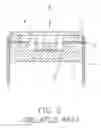
Semiconductor packages, such as a sensor package tend to be small and highly-integrated. Referring to FIG. 3, a typical sensor package 10 includes a substrate 1, a plurality of conductive pads 2, a semiconductor chip 3, and a plurality of wires 4, a plurality of conductive pins 5, a spacer 6, and a glass cover plate 7. A recess 8 is defined in the substrate 1 for accommodating the semiconductor chip 3. One terminal of each wire 4 is electrically connected to the semiconductor chip 3, and another terminal of each wire 4 is electrically connected to each conductive pad 2, and the plurality of conductive pads 2 are electrically connected to the plurality of conductive pins 5, respectively. The spacer 6 is arranged between the glass cover plate 7 and the conductive pad 2, and round the recess 8. The glass cover plate 7 is attached to the spacer 6 in a manner that the semiconductor chip 3 is sealed by glass cover plate 7.
However, a substrate 1 is needed for supporting and accommodating the semiconductor chip 3. Therefore, weight and volume of the sensor package 10 is increased.
What is needed, therefore, is to provided a sensor package with decreased weight and volume.
SUMMARY
The present invention relates to a sensor package. The sensor package includes an image sensing chip having a front surface, a plurality of bumps, a glass cover plate, and a connector. The plurality of bumps are formed on the front surface, and are electrically connected to the image sensing chip. The glass cover plate has a bottom surface facing the front surface, and the glass cover plate has a plurality of transparent conductive wires formed on the bottom surface. A terminal of each of the transparent conductive wires is electrically connected to a respective bump, and another terminal of each of the transparent conductive wires extends out of an orthogonal projection area of the image sensing chip on the bottom surface. The connector is electrically connected to the another terminal of each of the transparent conductive wires.
Other advantages and novel features of the present invention will become more apparent from the following detailed description of present embodiment when taken in conjunction with the accompanying drawings, in which:
BRIEF DESCRIPTION OF THE DRAWINGS
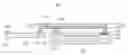
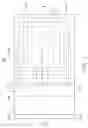
FIG. 1 is a plane view of a sensor package, in accordance with a present embodiment;
FIG. 2 is a cross-sectional view taken along line II-II of FIG. 1; and
FIG. 3 is a schematic, cross-sectional view of a typical sensor package.
DETAILED DESCRIPTION OF THE EMBODIMENT
Reference will now be made to the figures to describe the at least one present embodiment in detail.
Referring to FIGS. 1 and 2, a sensor package 100, according to a present embodiment, is shown. The sensor package 100 includes an image sensing chip 110, a plurality of bumps 120, a glass cover plate 140, and a connector 150.
The image sensing chip 110 is a complementary metal-oxide semiconductor (CMOS) or a charge-coupled device (CCD) for converting light signals into electrical signals. The image sensing chip 110 includes a front surface 112, and has a sensing area 114 for receiving light on the front surface 112. The image sensing chip 110 is provided with a plurality of soldering pads 116 on the front surface 112, and round the sensing area 114. Beneficially, quantity of the soldering pads 116 is same as that of the bumps 120. For preventing the sensing area 114 from accumulating dust, a first insulated adhesive 124 is arranged around the sensing area 114; and the glass cover plate 140, the first insulated adhesive 124, and the plurality of bumps 120 cooperatively seal the sensing area 114. Each bump 120 is a metallic bump.
The glass cover plate 140 includes a substrate 142 and a plurality of transparent conductive wires 146. The substrate 142 includes a bottom surface 144 facing the front surface 112 of the image sensing chip 110, and the plurality of transparent conductive wires 146 are formed on the bottom surface 144 so that some of the conductive wires 146 go across a part of the bottom surface 144 that faces toward sensing area 114. A length of the glass cover plate 140 along a cross-sectional view, as shown in FIG. 2, is greater than that of the image sensing chip 110. Therefore, a terminal of each transparent conductive wire 146 extends out of an orthogonal projection area of the image sensing chip 110 on the bottom surface 144, also as shown in FIG. 2. The plurality of conductive wires 146 are electrically connected to the plurality of bumps 120, and the plurality of bumps 120 and the first insulated adhesive 124 cooperatively make the image sensing chip 110 electrically and firmly attached to the glass cover plate 140. A material of the transparent conductive wires 146 is indium tin oxide (ITO) or carbon nanotubes.
The connector 150 includes a first connecting end 152 and a second connecting end 154. The connector 150 has a joint 158 arranged on the second connecting end 154, and has a plurality of connecting pads 156 spaced from each other on the first connecting end 152. The joint 158 is configured for being connected to a main circuit board (not shown) of an electronic device. The plurality of connecting pads 156 are electrically connected to the plurality of bumps 120 via the plurality of transparent conductive wires 146 respectively. For better structural connections, a second insulated adhesive 153 is filled in spaces between the plurality of connecting pads 146. Beneficially, the connector 150 is a flexible printed circuit board (FPCB).
Since the transparent conductive wires 146 are used in the sensor package 100, a substrate for supporting the image sensing chip 110 may be omitted from the sensor package 100. Therefore, weight and volume of the sensor package 100 is decreased.
It is to be understood, however, that even though numerous characteristics and advantages of the present invention have been set forth in the foregoing description, together with details of the structure and function of the invention, the disclosure is illustrative only, and changes may be made in detail, especially in matters of shape, size, and arrangement of parts within the principles of the invention to the full extent indicated by the broad general meaning of the terms in which the appended claims are expressed.
Claims
What is claimed is:1. A sensor package, comprising:
an image sensing chip having a front surface;
a plurality of bumps being formed on the front surface, and electrically connected to the image sensing chip;
a glass cover plate having a bottom surface facing the front surface, the glass cover plate having a plurality of transparent conductive wires formed on the bottom surface, a terminal of each of the transparent conductive wires being electrically connected to a respective bump, another terminal of each of the transparent conductive wires extending out of an orthogonal projection area of the image sensing chip on the bottom surface; and
a connector being electrically connected to the another terminal of each of the transparent conductive wires.
2. The sensor package as claimed in claim 1, wherein the image sensing chip has a sensing area for converting light signals into electrical signals on the front surface.
3. The sensor package as claimed in claim 2, further comprising a first insulated adhesive being arranged round the sensing area, and the glass cover plate, and wherein the first insulated adhesive, and the plurality of bumps cooperatively seal the sensing area.
4. The sensor package as claimed in claim 2, wherein the plurality of transparent conductive wires are formed on the bottom surface so that some of the conductive wires go across a part of the bottom surface that faces toward the sensing area.
5. The sensor package as claimed in claim 1, wherein the connector includes a plurality of connecting pads electrically connected to the plurality of transparent conductive wires respectively.
6. The sensor package as claimed in claim 5, further comprising a second insulated adhesive filled in spaces between the plurality of connecting pads.
7. The sensor package as claimed in claim 1, wherein a material of the plurality of transparent conductive wires is indium tin oxide or carbon nanotubes.
8. The sensor package as claimed in claim 1, wherein the plurality of bumps is metallic bumps.
Images & Drawings included:

Sources:
- United States Patent and Trademark Office - verify current appl. status at the USPTO↗
Similar patent applications:
- » 20250231337
SENSOR PACKAGE, METHOD FOR ATTACHING SENSOR PACKAGE, SET INCLUDING SENSOR PACKAGE AND CURING AGENT, AND BONDED STRUCTURE - » 20120324608
Mount for a scanning probe sensor package, scanning probe sensor package, scanning probe microscope and method of mounting or dismounting a scanning probe sensor package - » 20220082454
Sensor package and sensor package module including the same - » 20230119690
Fingerprint sensor package and sensor package - » 20250201725
FINGERPRINT SENSOR PACKAGE, FINGERPRINT SENSOR PACKAGE STACKED STRUCTURE AND FINGERPRINT AUTHENTICATION CARD - » 20220267142
Sensor package substrate, sensor module having the same, and sensor package substrate manufacturing method - » 20200343284
Image sensor packaging method, image sensor packaging structure, and lens module - » 20140124958
Sensor packaging method and sensor packages - » 20190123081
Image sensor packaging method, image sensor package and lens module - » 20140061948
Sensor packaging method and sensor packages
Recent applications in this class:
- » 20250261311 2025-08-14
DISPLAY PANEL AND DISPLAY APPARATUS - » 20250234460 2025-07-17
ELECTRONIC COMPONENTS - » 20250107000 2025-03-27
FLEXIBLE CIRCUIT FILM AND DISPLAY APPARATUS HAVING THE SAME - » 20250098070 2025-03-20
CIRCUIT BOARD ASSEMBLY AND ELECTRONIC DEVICE - » 20250024607 2025-01-16
CIRCUIT BOARD AND DISPLAY MODULE - » 20250008658 2025-01-02
DISPLAY DEVICE INCLUDING A FLEXIBLE CIRCUIT BOARD - » 20240431028 2024-12-26
ELECTRONIC DEVICE INCLUDING A PLURALITY OF FLEXIBLE PRINTED CIRCUIT BOARDS - » 20240397626 2024-11-28
Display Panel and Display Apparatus - » 20240389236 2024-11-21
CIRCUIT BOARD ASSEMBLY, DISPLAY MODULE AND MANUFACTURING METHOD THEREFOR, AND DISPLAY APPARATUS - » 20240284597 2024-08-22
DRIVE UNIT AND ELECTRICALLY ASSISTED BICYCLE
Recent applications for this Assignee:
- » 20140233961 2014-08-21
Optical communication module including optical-electrical signal converters and optical signal generators - » 20140083669 2014-03-27
HEAT SINK - » 20140063746 2014-03-06
Electronic device with heat dissipation assembly - » 20140061224 2014-03-06
AUTOMATIC VENDING MACHINE - » 20140060914 2014-03-06
Enclosure with shield apparatus - » 20140058727 2014-02-27
MULTIMEDIA RECORDING SYSTEM AND METHOD - » 20140055955 2014-02-27
Fastener - » 20140055322 2014-02-27
DISPLAY SYSTEM AND HEAD-MOUNTED DISPLAY APPARATUS - » 20140054439 2014-02-27
CONTAINER DATA CENTER WITH SUPPORTING APPARATUS - » 20140054311 2014-02-27
AUTOMATIC VENDING MACHINE WITH MOVING MEMBER FOR PRODUCTS