Method for suppressing lattice defects in a semiconductor substrate
US20090108293A1
2009-04-30
11/928,142
2007-10-30
✅ Patent granted
US 9,472,423 B2
2016-10-18
-
-
Daniel Whalen
Haynes Beffel & Wolfeld LLP
2030-07-07
Abstract:
A method for suppressing the formation of leakage-promoting defects in a crystal lattice following dopant implantation in the lattice. The process provides a compressive layer of atoms, these atoms having a size greater than that of the lattice member atoms. The lattice is then annealed for a time sufficient for interstitial defect atoms to be emitted from the compressive layer, and in that manner energetically stable defects are formed in the lattice at a distance from the compressive layer.
Inventors:
- Dipankar Pramanik 125 🇺🇸 Saratoga, CA, United States
- VICTOR MOROZ 164 🇺🇸 Saratoga, CA, United States
Assignee:
- SYNOPSYS INC. 2,038 🇺🇸 Mountain View, CA, United States
Applicant:
Interested in similar patents?
Get notified when new applications in this technology area are published.
Classification:
H01L29/778 IPC
Semiconductor devices adapted for rectifying, amplifying, oscillating or switching, or capacitors or resistors with at least one potential-jump barrier or surface barrier, e.g. PN junction depletion layer or carrier concentration layer; Details of semiconductor bodies or of electrodes thereof; Multistep manufacturing processes therefor; Types of semiconductor device ; Multistep manufacturing processes therefor controllable by only the electric current supplied, or only the electric potential applied, to an electrode which does not carry the current to be rectified, amplified or switched; Unipolar devices, e.g. field effect transistors; Field effect transistors with two-dimensional charge carrier gas channel, e.g. HEMT ; with two-dimensional charge-carrier layer formed at a heterojunction interface
H01L21/225 IPC
Processes or apparatus adapted for the manufacture or treatment of semiconductor or solid state devices or of parts thereof; Manufacture or treatment of semiconductor devices or of parts thereof the devices having at least one potential-jump barrier or surface barrier, e.g. PN junction, depletion layer or carrier concentration layer the devices having semiconductor bodies comprising elements of Group IV of the Periodic System or AB compounds with or without impurities, e.g. doping materials; Diffusion of impurity materials, e.g. doping materials, electrode materials, into or out of a semiconductor body, or between semiconductor regions; Interactions between two or more impurities; Redistribution of impurities using diffusion into or out of a solid from or into a solid phase, e.g. a doped oxide layer
H01L29/1079 » CPC further
Semiconductor devices adapted for rectifying, amplifying, oscillating or switching, or capacitors or resistors with at least one potential-jump barrier or surface barrier, e.g. PN junction depletion layer or carrier concentration layer; Details of semiconductor bodies or of electrodes thereof; Multistep manufacturing processes therefor; Semiconductor bodies ; Multistep manufacturing processes therefor characterised by their shape; characterised by the shapes, relative sizes, or dispositions of the semiconductor regions ; characterised by the concentration or distribution of impurities within semiconductor regions with semiconductor regions connected to an electrode not carrying current to be rectified, amplified or switched and such electrode being part of a semiconductor device which comprises three or more electrodes; Substrate region of field-effect devices of field-effect transistors with insulated gate
H01L21/324 » CPC main
Processes or apparatus adapted for the manufacture or treatment of semiconductor or solid state devices or of parts thereof; Manufacture or treatment of semiconductor devices or of parts thereof the devices having at least one potential-jump barrier or surface barrier, e.g. PN junction, depletion layer or carrier concentration layer the devices having semiconductor bodies comprising elements of Group IV of the Periodic System or AB compounds with or without impurities, e.g. doping materials; Treatment of semiconductor bodies using processes or apparatus not provided for in groups - Thermal treatment for modifying the properties of semiconductor bodies, e.g. annealing, sintering
H01L21/265 IPC
Processes or apparatus adapted for the manufacture or treatment of semiconductor or solid state devices or of parts thereof; Manufacture or treatment of semiconductor devices or of parts thereof the devices having at least one potential-jump barrier or surface barrier, e.g. PN junction, depletion layer or carrier concentration layer the devices having semiconductor bodies comprising elements of Group IV of the Periodic System or AB compounds with or without impurities, e.g. doping materials; Bombardment with radiation with high-energy radiation producing ion implantation
H01L29/10 IPC
Semiconductor devices adapted for rectifying, amplifying, oscillating or switching, or capacitors or resistors with at least one potential-jump barrier or surface barrier, e.g. PN junction depletion layer or carrier concentration layer; Details of semiconductor bodies or of electrodes thereof; Multistep manufacturing processes therefor; Semiconductor bodies ; Multistep manufacturing processes therefor characterised by their shape; characterised by the shapes, relative sizes, or dispositions of the semiconductor regions ; characterised by the concentration or distribution of impurities within semiconductor regions with semiconductor regions connected to an electrode not carrying current to be rectified, amplified or switched and such electrode being part of a semiconductor device which comprises three or more electrodes
H01L29/78 IPC
Semiconductor devices adapted for rectifying, amplifying, oscillating or switching, or capacitors or resistors with at least one potential-jump barrier or surface barrier, e.g. PN junction depletion layer or carrier concentration layer; Details of semiconductor bodies or of electrodes thereof; Multistep manufacturing processes therefor; Types of semiconductor device ; Multistep manufacturing processes therefor controllable by only the electric current supplied, or only the electric potential applied, to an electrode which does not carry the current to be rectified, amplified or switched; Unipolar devices, e.g. field effect transistors; Field effect transistors with field effect produced by an insulated gate
Description
BACKGROUND OF THE INVENTION
The present invention relates to the field of semiconductor fabrication. In particular, it relates to the fabrication of field effect transistors (FETs), involving the formation of semiconductor materials of selected conductivity, carried on by implantation of dopants.
Fabrication of metal oxide semiconductor (MOS) FETs requires the formation of source and drain regions in a substrate of generally pure silicon (Si). The Si is provided in the form of a wafer, grown as a single crystal. Zones of the Si lattice are converted into regions of N or P conductivity by the addition of donor-type dopants, such as arsenic, for N regions, and acceptor-type dopants, such as boron, for P regions. These dopants are generally introduced by ion bombardment, in which ionized dopant atoms are energized and fired at the lattice, penetrating the crystal structure to a depth largely dependent on the bombardment energy and the ion mass.
It can be immediately gathered that such bombardment introduces crystal damage, in which lattice atoms are knocked out of lattice sites, while at the same time a certain number of the newly-introduced atoms will likewise come to rest in positions outside the lattice positions. Such out-of-position phenomena are termed defects. A vacant lattice site is termed a vacancy defect, while an atom located at a non-lattice site is referred to as an interstitial defect. The restorative method generally employed in the art consists of annealing the crystal, applying heat to the lattice to mildly energize the atoms, allowing them to work themselves back into the lattice structure, which provides the arrangement having the lowest overall energy level.
SUMMARY OF THE INVENTION
An aspect of the claimed invention is a method for suppressing the formation of leakage-promoting defects in a crystal lattice following dopant implantation in the lattice. The process provides a compressive layer of atoms, these atoms having a size greater than that of the lattice member atoms. The lattice is then annealed for a time sufficient for interstitial defect atoms to be emitted from the compressive layer, and in that manner energetically stable defects are formed in the lattice at a distance from the compressive layer.
BRIEF DESCRIPTION OF THE DRAWINGS
FIG. 1 illustrates manner in which the problem of stress-induced defect formation occurs in a semiconductor substrate.
FIG. 2 schematically depicts the solution of the claimed invention.
FIG. 3 illustrates the mechanism by which the method of the presently claimed invention suppresses defects in a semiconductor substrate.
FIG. 4 depicts an embodiment of a semiconductor formed in accordance with the claimed invention.
FIG. 5 depicts an alternate embodiment of a semiconductor formed in accordance with the claimed invention.
FIG. 6 depicts a further alternate embodiment of a semiconductor formed in accordance with the claimed invention.
DETAILED DESCRIPTION
The following detailed description is made with reference to the figures. Preferred embodiments are described to illustrate the present invention, not to limit its scope, which is defined by the claims. Those of ordinary skill in the art will recognize a variety of equivalent variations on the description that follows.
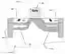
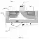
The problem addressed by the present disclosure is seen in FIG. 1, which depicts a typical MOSFET 100 after undergoing ion implantation. The transistor is formed on a silicon substrate 101 and includes source 102, drain 104 and gate 106. The depletion layer 108 adjacent each electrode and extending across the channel between the source and drain, is well known in the art. The depicted cell is one member of an array that can encompass millions of cells, as known in the art, and the cell is separated from other members of the array by Shallow Trench Isolators (STI) 109, filled with dielectric fill material.
The source and drain are formed in the silicon substrate by the implantation of dopants, as known in the art, and the implantation process produces defects in the lattice, which defects are addressed by annealing the substrate after implantation. While most defects are removed by annealing, some will coalesce into larger defects 112, often in the form of dislocation loops or area defects. These defects are generally collections of interstitial silicon atoms, knocked out of their lattice positions by dopant atoms. It has been found that large defects 112 tend to form more readily in portions of the substrate that either have no mechanical stress on the lattice, or preferably, where the lattice is subjected to tensile stress. For example, locations where the lattice passes around a convex point in an underlying strained structure, such as around corners in the SiGe source, SiGe drain and STI's, tend to favor the accumulation of defects, resulting in the situation seen in FIG. 1, where defects 112 are seen at the corners of the source and drain as well as the corners of the STI's.
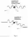
FIG. 2 illustrates an analogy to the mechanism at work in this situation. In each portion of the drawing, the lattice 200 is represented as having lattice sites, corresponding to the peaks in the figure, where an interstitial atom 201 can come to rest in between the lattice atoms, requiring some expenditure of energy to move to another interstitial position. In the upper portion of the drawing, the energy required to move to either side is identical, corresponding to the situation in an unstressed lattice. Probabilities of moving either left or right in the drawing are equal. The bottom portion of the drawing, however, shows one end of the line is higher than the other, analogous to the situation in which one portion of the lattice is subjected to compressive stress and the other is relaxed. Here, movement “uphill” toward the compressive stress clearly requires more energy than movement “downhill” toward the relaxed portion of the lattice. Thus, movement toward relaxed portions of the lattice, such as locations where the lattice is stressed by bending around a corner, are energetically favorable and will tend to collect more defects than compressively stressed areas.
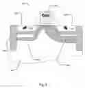
A conceptual view of the operation of the claimed invention is seen in FIG. 3. There, along with the implantation of dopants, a compressive layer 103 of atoms having a larger size than silicon, being higher on the periodic table, is implanted in the substrate. Germanium, lying directly below silicon in the periodic table, is a preferred element for this purpose. That layer produces an area of higher compression, causing a net migration of defects away from the compressive layer, indicated by arrows 105. After annealing, the structure formed by this process contains a number of large defects 112, in the form of area, line or dislocation loop defects, but all such defects occur outside the compressive layer.
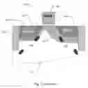
FIG. 4 illustrates an embodiment of the presently claimed invention in a transistor 100, with elements as set out above in connection with FIG. 1. Here, however, a compressive layer 103 of germanium is formed along with the dopant atoms. The germanium can be co-implanted—implanted at the same time—along with the dopants, or a layer of Ge can be epitaxially grown during formation of the substrate. Both of these techniques are effective in the illustrated context, and both are well-known in the art. Neither is particularly preferred, and thus the user can choose which process to employ based on other factors.
Most importantly, defects 112 are all located outside the compressive layer, and thus away from the depletion layer 108. Confined to portions of the substrate where they cannot form a leakage path, these defects are rendered entirely harmless.
An alternative embodiment locates the compressive layer at least partially within the depletion layer, as seen in FIG. 4. The exact position can lie entirely within the layer, or overlapping it. The primary goal of the compressive layer is to protect the depletion layer from defect formation, so having the compressive layer within the depletion layer altogether prevents the formation of defects there.
The optimum solution calls for the compressive layer 103 to lie entirely outside the depletion layer, between the depletion layer and the defects 112, as shown in FIG. 5. There, the compressive layer is positioned to prevent the movement of intersitials toward or into the depletion layer, completely precluding defect formation there.
Another embodiment, shown in FIG. 6, positions the compressive layer 103 at a level shallower than that of the depletion layer 108. Here, those in the art will understand that it would not be desirable to have the compressive layer extend into channel, and thus the compressive layer would be implanted after implantation of the source and drain regions 102 and 104, and like those operations, the gate structure would be employed as a mask, as known in the art. Thus, the compressive layer would lie wholly within the source and drain regions, as shown. As will be understood, the shape of the compressive layer will have substantially the same profile as does the source or drain region containing that layer, a fact that may not be clear from the drawing. Here, defects would form in the source and drain regions.
While the present invention is disclosed by reference to the preferred embodiments and examples detailed above, it is understood that these examples are intended in an illustrative rather than in a limiting sense. It is contemplated that modifications and combinations will readily occur to those skilled in the art, which modifications and combinations will be within the spirit of the invention and the scope of the following claims.
Claims
1. During fabrication of a semiconductor on a crystal substrate, the semiconductor having N-type and P-type regions, with a channel between the source and drain regions and a gate positioned above the channel, and having a depletion layer adjacent each region, a method for suppressing the formation of leakage-promoting defects in a crystal lattice following dopant implantation in the lattice, comprising the steps of
providing a compressive layer of atoms, such atoms being selected to impose a compressive stress on the crystal lattice;
annealing the lattice for a time sufficient for interstitial defect atoms to be emitted from the compressive layer;
whereby energetically stable defects are formed in the lattice at a distance from the compressive layer.
2. The method of claim 1, wherein the compressive layer atoms are larger than the lattice member atoms.
3. The method of claim 1, wherein the compressive atoms are electrically neutral.
4. The method of claim 1, wherein the compressive layer is provided by co-implantation of compressive atoms with dopant atoms.
5. The method of claim 1, wherein the compressive layer is provided by epitaxially growing the compressive layer.
6. The method of claim 1, wherein the lattice-member atoms are silicon, and the compressive layer atoms are germanium.
17. The semiconductor of claim 10, wherein the compressive layer lies outside the depletion layer, between the depletion layer and the defects.
18. The semiconductor of claim 10, wherein the compressive layer lies at a level shallower than that of the depletion layer, such that the defects lie in the source and drain regions
7. The method of claim 1, wherein the compressive layer is provided at least partially within the depletion layer.
8. The method of claim 1, wherein the compressive layer is provided outside the depletion layer, between the depletion layer and the defects
9. The method of claim 1, wherein the compressive layer is provided at a level shallower than that of the depletion layer, such that the defects lie in the source and drain regions.
10. A semiconductor formed on a crystal substrate, having N-type and P-type regions, with a channel between the source and drain regions and a gate positioned above the channel, and having a depletion layer adjacent each region, comprising a compressive layer of atoms, such atoms being selected to impose a compressive stress on the crystal lattice, wherein any existing energetically stable lattice defects, lie outside the compressive layer.
11. The semiconductor of claim 10, wherein the compressive layer atoms are larger than the lattice member atoms.
12. The semiconductor of claim 10, wherein the compressive layer atoms are electrically neutral
13. The semiconductor of claim 10, wherein the compressive layer is provided by co-implantation of compressive atoms with dopant atoms.
14. The semiconductor of claim 10, wherein the compressive layer is provided by epitaxially growing the compressive layer.
15. The semiconductor of claim 10, wherein the lattice-member atoms are silicon, and the compressive layer atoms are germanium.
16. The semiconductor of claim 10, wherein the compressive layer lies at least partially within the depletion layer.
Images & Drawings included:

Sources:
- United States Patent and Trademark Office - verify current appl. status at the USPTO↗
Similar patent applications:
Recent applications in this class:
- » 20250293047 2025-09-18
SEMICONDUCTOR DEVICE AND METHOD OF REPAIRING WAFER - » 20250201580 2025-06-19
METHOD OF MANUFACTURING SEMICONDUCTOR DEVICE - » 20250149344 2025-05-08
METHOD FOR FABRICATING SEMICONDUCTOR DEVICE - » 20250118572 2025-04-10
ANNEAL CHAMBER - » 20250105022 2025-03-27
METHOD OF MANUFACTURING SEMICONDUCTOR DEVICES AND VERTICAL POWER SEMICONDUCTOR DEVICE - » 20250096007 2025-03-20
SUBSTRATE TREATING APPARATUS AND SUBSTRATE TREATING METHOD - » 20250079186 2025-03-06
Opaque Thermal Layer for Silicon Carbide Substrates - » 20250079185 2025-03-06
METHOD OF BONDING SEMICONDUCTOR MATERIALS AND STRUCTURE FORMED BY THE SAME - » 20250054772 2025-02-13
HEAT TREATMENT METHOD FOR HEATING SUBSTRATE BY LIGHT IRRADIATION - » 20250022720 2025-01-16
TEMPERATURE CONTROL METHOD FOR SEMICONDUCTOR PROCESS
Recent applications for this Assignee:
- » 20240111660 2024-04-04
Managing high performance simulation representation of an emulation system - » 20240103761 2024-03-28
Buffer circuitry for store to load forwarding - » 20230352069 2023-11-02
ON-CHIP AUTOMATION OF CLOCK-TO-Q ACCESS TIME MEASUREMENT OF A MEMORY DEVICE - » 20230214574 2023-07-06
EXTENDED REGULAR EXPRESSION MATCHING IN A DIRECTED ACYCLIC GRAPH BY USING ASSERTION SIMULATION - » 20230206970 2023-06-29
SRAM non-clamping write driver with write assist - » 20230163032 2023-05-25
Forming a wrap-around contact to connect a source or drain epitaxial growth of a complimentary field effect transistor (CFET) to a buried power rail (BPR) of the CFET - » 20230154751 2023-05-18
Fabrication technique for forming ultra-high density integrated circuit components - » 20230086197 2023-03-23
Verification of Ethernet hardware based on checksum correction with cyclic redundancy check - » 20230065867 2023-03-02
Memory optimization for storing objects in nested hash maps used in electronic design automation systems - » 20230063149 2023-03-02
Low-area, wide range clocking scheme using inductance/capacitance oscillators