Multilayer structural body and method for cleaning the same
US20090133713A1
2009-05-28
11/988,648
2006-07-12
Abstract:
It has been difficult to provide a large-sized ceramic member quickly and economically. A multilayer structure is produced by forming a ceramic film on a base which is made of a material that can be shaped comparatively easily. The ceramic film is formed by a plasma spraying method, CVD method, PVD method, sol-gel method or the like. Alternatively, the ceramic film may be formed by a method combined with a spray deposit film.
Inventors:
- Tadahiro OHMI 230 🇯🇵 Miyagi, Japan
- Akinobu TERAMOTO 75 🇯🇵 Miyagi, Japan
- Hitoshi Morinaga 6 🇯🇵 Miyagi, Japan
- Yoshihumi Tsutai 2 🇯🇵 Miyagi, Japan
- Yukio Kishi 3 🇯🇵 Miyagi, Japan
- Hiromichi Ohtaki 1 🇯🇵 Miyagi, Japan
Interested in similar patents?
Get notified when new applications in this technology area are published.
Classification:
C23C4/00 » CPC main
Coating by spraying the coating material in the molten state, e.g. by flame, plasma or electric discharge
B08B3/02 » CPC further
Cleaning by methods involving the use or presence of liquid or steam Cleaning by the force of jets or sprays
C23C4/02 » CPC further
Coating by spraying the coating material in the molten state, e.g. by flame, plasma or electric discharge Pretreatment of the material to be coated, e.g. for coating on selected surface areas
C23C4/11 » CPC further
Coating by spraying the coating material in the molten state, e.g. by flame, plasma or electric discharge characterised by the coating material; Oxides, borides, carbides, nitrides or silicides; Mixtures thereof Oxides
C23C16/405 » CPC further
Chemical coating by decomposition of gaseous compounds, without leaving reaction products of surface material in the coating, i.e. chemical vapour deposition [CVD] processes characterised by the deposition of inorganic material, other than metallic material; Deposition of compounds, mixtures or solid solutions, e.g. borides, carbides, nitrides; Oxides of refractory metals or yttrium
B08B3/12 » CPC further
Cleaning by methods involving the use or presence of liquid or steam; Cleaning involving contact with liquid with additional treatment of the liquid or of the object being cleaned, e.g. by heat, by electricity, by vibration by sonic or ultrasonic vibrations
C23C16/545 » CPC further
Chemical coating by decomposition of gaseous compounds, without leaving reaction products of surface material in the coating, i.e. chemical vapour deposition [CVD] processes characterised by the method of coating; Apparatus specially adapted for continuous coating for coating elongated substrates
C23C26/00 » CPC further
Coating not provided for in groups -
C23C28/04 » CPC further
Coating for obtaining at least two superposed coatings either by methods not provided for in a single one of groups - or by combinations of methods provided for in subclasses and or only coatings of inorganic non-metallic material
B08B2203/0288 » CPC further
Details of cleaning machines or methods involving the use or presence of liquid or steam; Details of machines or methods for cleaning by the force of jets or sprays Ultra or megasonic jets
Y10T428/25 » CPC further
Stock material or miscellaneous articles Web or sheet containing structurally defined element or component and including a second component containing structurally defined particles
Y10T428/252 » CPC further
Stock material or miscellaneous articles; Web or sheet containing structurally defined element or component and including a second component containing structurally defined particles Glass or ceramic [i.e., fired or glazed clay, cement, etc.] [porcelain, quartz, etc.]
B32B5/16 IPC
Layered products characterised by the non- homogeneity or physical structure, i.e. comprising a fibrous, filamentary, particulate or foam layer; Layered products characterised by having a layer differing constitutionally or physically in different parts characterised by features of a layer formed of particles, e.g. chips, powder or granules
Description
TECHNICAL FIELD
This invention relates to a structural body used as a component or a member for use in an environment where high cleanness is required, such as in the dry process for electronic devices, the manufacture of medical supplies, or the processing/manufacture of foodstuffs, and to a cleaning method therefor.
BACKGROUND ART
The miniaturization of the design rule of semiconductors has been advanced following the improvement in integration thereof and thus it has been required to reduce the allowable size and amount of adhering substance and metal contaminants. Further, in terms of sanitation of medical supplies, foodstuffs, and so on, it is required to reduce adhering substance and metal contaminants. Normally, structural bodies that hate metal contaminants or the like employ ceramics as members thereof. Particularly, structural bodies forming semiconductor and liquid-crystal manufacturing apparatuses tend to increase in size following the increase in size of wafers and panels.
Herein, an explanation will be given using a microwave plasma processing apparatus as an example of a semiconductor manufacturing apparatus. The microwave plasma processing apparatus comprises a process chamber, a holding stage disposed in the process chamber for holding a processing substrate, a shower plate provided at a position facing the processing substrate, a cover plate disposed on the shower plate, and a radial line slot antenna provided on the cover plate. The shower plate is in the form of a plate made of alumina and having a number of gas ejection holes, while the cover plate is also made of alumina. Further, it is considered that the inner wall of the process chamber is also made of alumina or is made of yttria in terms of corrosion resistance to plasma.
It has been pointed out that, in the case where various members in a semiconductor manufacturing apparatus are formed of a ceramic such as alumina as described above, the ceramic members are subjected to formation of organic contaminants, metal contaminants, and contaminants due to adhesion of particles in various manufacturing processes such as baking, grinding, and polishing. If a wafer or a liquid crystal panel is brought into direct contact with such a member with the contaminants remaining thereon, the contaminants are accumulated on the surface of the wafer or the liquid crystal panel to cause a circuit failure. It has also been pointed out that the impurities diffuse into the wafer due to the contact.
Therefore, it is necessary to suppress adhesion of particles and metals as much as possible in order to obtain semiconductors or liquid crystal panels with high yield.
The requirement for high cleanness of various members forming semiconductor manufacturing apparatuses tends to be further increased in future along with the increase in size of wafers and liquid crystal panels.
The present inventors have previously proposed a method of cleaning ceramic members forming various members of a semiconductor manufacturing apparatus in Patent Document 1. According to this cleaning method, it is possible to clean the surface of the ceramic member. Specifically, the ceramic member cleaning method proposed in Patent Document 1 performs precleaning of the ceramic member by at least one method among wiping with a highly clean sponge or brush, ultrasonic cleaning with a degreaser, immersion cleaning with an organic chemical, ultrasonic cleaning with ozone water, SPM cleaning, and HF/HNO3 cleaning.
Further, this cleaning method performs, after the precleaning, cleaning with ozone water, ultrasonic cleaning with pure water containing hydrogen and controlled at an alkaline pH, and cleaning with at least one selected from HF, SPM, HPM, and HNO3/HF and finally performs ultrasonic cleaning using one kind selected from pure water containing hydrogen, ozone water, and ultrapure water.
By cleaning the ceramic member using the foregoing cleaning method, the number of particles having a particle size of 0.2 μm or more on the surface of the ceramic member can be reduced to two or less per mm2.
Therefore, since the surface of the ceramic member cleaned according to Patent Document 1 is extremely clean, it is possible to significantly improve the yield of wafers or liquid crystal panels.
As described above, along with the increase in size of semiconductor manufacturing apparatuses, various ceramic members for use in those semiconductor manufacturing apparatuses unavoidably increase in size. However, since a ceramic member is manufactured by baking at a high temperature of 1000° C. or more, shrinkage unavoidably occurs during the baking. As a result, it becomes more difficult to achieve dimensional accuracy as the ceramic member increases in size. Further, as the ceramic member increases in size, the baking is required for a longer time. Therefore, it is difficult to manufacture a ceramic member that is large in size and still has precise dimensions, in a short time and economically.
Therefore, the current situation is that it is practically difficult to quickly respond to the requirement for increase in size using a ceramic member alone.
- Patent Document 1: Japanese Unexamined Patent Application Publication (JP-A) No. 2004-279481
- Patent Document 2: Japanese Unexamined Patent Application Publication (JP-A) No. H5-339699
- Patent Document 3: Japanese Unexamined Patent Application Publication (JP-A) No. H5-202460
DISCLOSURE OF THE INVENTION
Problem to be Solved by the Invention
It is an object of this invention to provide, in response to the requirement for increase in size of semiconductor manufacturing apparatuses and so on, a structural body that exhibits functions and effects, for example, insulating properties, corrosion resistance in etching environment, and weight lightening, equivalent to a ceramic member and has an extremely clean surface.
It is another object of this invention to provide a structural body having a multilayer structure in order to reduce a burden in the case where a member of a semiconductor manufacturing apparatus or the like is formed by a ceramic member alone.
It is still another object of this invention to provide a multilayer structural body having a surface layer that is not subjected to stripping or the like even if cleaning is performed for increasing the cleanness.
It is a further object of this invention to provide a method of depositing a ceramic layer with a high adhesion strength as a surface layer forming the surface of a multilayer structural body.
It is another subject of this invention to provide a cleaning method for obtaining a ceramic surface with a high cleanness.
Means for Solving the Problem
The present inventors have made a study of a structural body with a multilayer structure instead of forming a ceramic member for a semiconductor manufacturing apparatus by a ceramic member alone. Specifically, the present inventors have examined a multilayer structural body in which a film (specifically a ceramic film) is deposited on a base member, and have found that, by improving a deposition method and a cleaning method for the ceramic film deposited on the base member, there is obtained a structural body having a surface equivalent to that of the ceramic member shown in Patent Document 1.
According to a first aspect of the present invention, there is provided a multilayer structural body, which comprises a base member and a film formed on a surface of the base member, wherein the number of adhering particles having a particle size of 0.2 μm or more is two or less per mm2 on the film.
According to a second aspect of the present invention, there is provided the multilayer structural body of the first aspect, wherein the base member is formed of a ceramic, a metal, or a composite material thereof.
According to a third aspect of the present invention, there is provided the multilayer structural body of the second aspect, wherein the film is a ceramic film.
According to a fourth aspect of the present invention, there is provided the multilayer structural body of the third aspect, wherein the ceramic film is a sprayed film deposited on the base member by spraying.
According to a fifth aspect of the present invention, there is provided the multilayer structural body of the fourth aspect, wherein the ceramic film is deposited on the base member by a CVD method.
According to a sixth aspect of the present invention, there is provided the multilayer structural body mentioned above, wherein the ceramic film is deposited on the base member by a PVD method.
According to a seventh aspect of the present invention, there is provided the multilayer structural body mentioned above, wherein the ceramic film is deposited on the base member by a sol-gel method.
According to an eighth aspect of the present invention, there is provided the multilayer structural body mentioned above, wherein the ceramic film is formed on a sprayed film by any one of the methods according to claims 5 to 7
According to a ninth aspect of the present invention, there is provided the multilayer structural body mentioned above, wherein the ceramic film has an adhesion strength of 10 MPa or more.
According to a tenth aspect of the present invention, there is provided a method of cleaning a multilayer structural body. The multilayer structural body includes a base member and a film formed on a surface of the base member. The method includes a step of cleaning the film by applying an ultrasonic wave of 5 W/cm2 or more and less than 30 W/cm2.
According to an eleventh aspect of the present invention, there is provided the method mentioned above, wherein the ultrasonic cleaning is performed using a nozzle-type cleaning apparatus.
According to a twelfth aspect of the present invention, there is provided the method according to the tenth or the eleventh aspect, wherein the ultrasonic cleaning is performed by preparing a solution in which a gas selected from the group consisting of hydrogen, ammonia, and carbon dioxide is dissolved in ultrapure water, and applying the ultrasonic wave to the solution.
EFFECT OF THE INVENTION
According to this invention, by providing a laminated structural body having a ceramic layer at its surface, there is an effect that it is possible to quickly and economically cope with an increase in size of a structural member. Further, since high-cleanness cleaning can be performed for the ceramic layer deposited on a base member, high cleanness can be maintained. Further, since the adhesion strength of the deposited ceramic layer is high, even if an ultrasonic wave of 5 W/cm2 or more and 30 W/cm2 or less is applied in the high-cleanness cleaning, there is no occurrence of stripping or the like.
BRIEF DESCRIPTION OF THE DRAWINGS
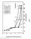
FIG. 1 is a relational diagram between the number of particles and the ultrasonic output in high-cleanness cleaning of Y2O3 films obtained by various manufacturing methods according to this invention.
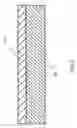
FIG. 2 is a sectional view of a multilayer structural body according to a first embodiment of this invention.
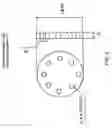
FIG. 3 is a sample shape diagram for measuring the number of adhering particles.
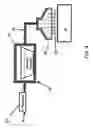
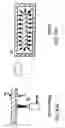
FIG. 4 is a schematic diagram explaining an atmosphere-open thermal CVD apparatus that forms a multilayer structural body according to a second embodiment of this invention.
FIGS. 5(a) and (b) are diagrams, in imitation of scanning electron microscope (SEM) photographs, showing a section and a plane of a multilayer structural body formed by the CVD apparatus shown in FIG. 3.
FIGS. 6(a) and (b) are diagrams explaining, in order of process, a sol-gel method that forms a multilayer structural body according to a third embodiment of this invention.
DESCRIPTION OF SYMBOLS
-
- 10 base member
- 11 ceramic layer
- 21 flowmeter
- 23 evaporator
- 25 nozzle
- 27 heater
- 29 heater
- 31 spray gun
- 33 ceramic precursor
- 35 oven
BEST MODE FOR CARRYING OUT THE INVENTION
Hereinbelow, embodiments of this invention will be described.
FIG. 1 is a relational diagram between the number of particles and the ultrasonic output in high-cleanness cleaning of Y2O3 films obtained by various manufacturing methods according to this invention. As shown in FIG. 1, since the adhesion strength of each deposited ceramic layer is high, even if an ultrasonic wave of 5 W/cm2 or more and 30 W/cm2 or less is applied for high-cleanness cleaning, there is no occurrence of stripping or the like.
Referring to FIG. 2, a multilayer structural body according to a first embodiment of this invention comprises, for example, a base member 10 and a ceramic layer 11 in the form of yttria deposited by plasma spraying (i.e. a plasma-sprayed Y2O3 layer) on the surface of the base member. Herein, an aluminum alloy with a diameter of 40 mm and a thickness of 3 mm is used as the base member 10 and the plasma-sprayed film is formed as the ceramic layer 11 on the surface of the base member 10. The illustrated plasma-sprayed film is the Y2O3 layer having a thickness of 200 μm. A spray apparatus described, for example, in Patent Document 2 or Patent Document 3 can be used for the plasma spraying.
A ceramic film is preferably Y2O3, Al2O3, MgO, or a compound thereof for a semiconductor manufacturing apparatus in terms of plasma resistance.
In the illustrated example, the ceramic layer 11 is directly formed on the surface of the aluminum alloy base member 10. However, the surface of the aluminum alloy base member 10 may be anodized to thereby form an anodized film and then a plasma-sprayed film may be formed. That is, a layer formed on the base member 10 may be a composite layer.
Normally, in the case of a plasma-sprayed film formed by plasma spraying, a dense ceramic layer cannot be obtained and, therefore, since adhering substances and so on caused by manufacturing processes remain in pores by a normal cleaning method, it is unsuitable for forming a member that requires high quality. However, according to the study by the present inventors, there has been obtained a multilayer structural body that can sufficiently withstand use as a member of a semiconductor manufacturing apparatus without causing film stripping or defect, by a developed cleaning method.
Quantitative evaluation of particles was carried out in the following manner.
Using a sample with a shape shown in FIG. 3, a mirror-finished ceramic film surface was, before and after cleaning, subjected to adsorption/transfer onto a silicon wafer at 0.107 Pa (about 0.8 mTorr) or less for 2 minutes, thereby transferring adhering particles on the surface of the sample onto the wafer side. Thereafter, the particles on the silicon wafer were measured by a particle counter (Surfscan6420 manufactured by Tencor).
The cleaning was performed such that miscellaneous adhering substances that could be visually observed were first removed by ultrasonic cleaning in pure water and then cleaning comprising first to fourth cleaning processes was applied to the sample precleaned using a clean-room sponge and a degreaser. The first cleaning process is an organic substance removal process, wherein ozone-dissolved ultrapure water is effective. The second process is a process of cleaning by selecting at least one from methods of cleaning by a nozzle-type ultrasonic cleaning apparatus (abbreviated as nozzle) using ultrapure water in which a gas selected from the group consisting of hydrogen, ammonia, and carbon dioxide is dissolved and cleaning by a bath-type ultrasonic cleaning apparatus (abbreviated as bath) using the same ultrapure water. The third process is a metal removal process and the fourth process is a rinsing process which is rinsing with only ultrapure water or with ultrapure water in which a gas selected from the group consisting of hydrogen, ammonia, and carbon dioxide is dissolved.
Tables 1 to 4 below show the particle measurement results along with ultrasonic cleaning conditions applied to Examples of this invention, respectively.
| TABLE 1 | |||||||||
| Film | Ultrasonic | Number of | Film Defect | ||||||
| Forming | Base | Cleaning | Output | Particles | ∘: no | ||||
| No. | Method | Member | Film | Method | W/cm2 | particles/mm2 | x: yes | Classification | Remarks |
| 1 | spraying | Al alloy | Y2O3 | nozzle type | 1 | 4 | ∘ | Comparative | |
| Example | |||||||||
| 2 | 4 | 3.0 | ∘ | ||||||
| 3 | 5 | 1.1 | ∘ | Example | |||||
| 4 | 15 | 0.5 | ∘ | ||||||
| 5 | 30 | 0.4 | ∘ | ||||||
| 6 | 33 | 0.4 | x | Comparative | film stripping | ||||
| Example | |||||||||
| 7 | bath type | 1 | 5.0 | ∘ | |||||
| 8 | 4 | 3.0 | ∘ | ||||||
| 9 | 5 | 1.5 | ∘ | Example | |||||
| 10 | Al2O3 | nozzle | 4 | 3.0 | ∘ | Comparative | |||
| type | Example | ||||||||
| 11 | 5 | 1.3 | ∘ | Example | |||||
| 12 | 15 | 1.1 | ∘ | ||||||
| 13 | 30 | 1.0 | ∘ | ||||||
| 14 | 33 | 1.0 | x | Comparative | film stripping | ||||
| Example | |||||||||
| 15 | bath type | 1 | 4.5 | ∘ | |||||
| 16 | 4 | 3.0 | ∘ | ||||||
| 17 | 5 | 1.5 | ∘ | Example | |||||
| 18 | ceramic | Y2O3 | nozzle | 4 | 3.0 | ∘ | Comparative | ||
| type | Example | ||||||||
| 19 | 5 | 1.1 | ∘ | Example | |||||
| 20 | 15 | 0.7 | ∘ | ||||||
| 21 | bath type | 4 | 3.0 | ∘ | Comparative | ||||
| Example | |||||||||
| 22 | 5 | 1.5 | ∘ | Example | |||||
| 23 | metal- | Y2O3 | nozzle | 4 | 6.0 | ∘ | Comparative | ||
| ceramic | type | Example | |||||||
| 24 | composite | 5 | 2.0 | ∘ | Example | ||||
| 25 | material | 15 | 1.5 | ∘ | |||||
| 26 | 30 | 1.0 | ∘ | ||||||
| 27 | 33 | 1.0 | x | Comparative | film stripping | ||||
| Example | |||||||||
| TABLE 2 | |||||||||
| Film | Ultrasonic | Number of | Film Defect | ||||||
| Forming | Base | Cleaning | Output | Particles | ∘: no | ||||
| No. | Method | Member | Film | Method | W/cm2 | particles/mm2 | x: yes | Classification | Remarks |
| 28 | CVD | ceramics | Y2O3 | nozzle | 1 | 3.5 | — | Comparative | |
| type | Example | ||||||||
| 29 | 4 | 2.8 | ∘ | ||||||
| 30 | 5 | 2.0 | ∘ | Example | |||||
| 31 | 15 | 1.0 | ∘ | ||||||
| 32 | 30 | 0.5 | ∘ | ||||||
| 33 | 33 | 0.5 | x | Comparative | film stripping | ||||
| Example | |||||||||
| 34 | bath type | 4 | 3.0 | ∘ | |||||
| 35 | 5 | 2.0 | ∘ | Example | |||||
| 36 | Al2O3 | nozzle | 4 | 2.5 | ∘ | Comparative | |||
| type | Example | ||||||||
| 37 | 5 | 2.0 | ∘ | Example | |||||
| 38 | 15 | 0.5 | ∘ | ||||||
| 39 | Si | Y2O3 | 5 | 1.0 | ∘ | ||||
| 40 | 15 | 0.5 | ∘ | ||||||
| 41 | SUS | Y2O3 | 4 | 2.5 | ∘ | Comparative | |||
| Example | |||||||||
| 42 | 5 | 1.5 | ∘ | Example | |||||
| 43 | 15 | 0.5 | ∘ | ||||||
| 44 | bath type | 4 | 4.0 | ∘ | Comparative | ||||
| Example | |||||||||
| 45 | 5 | 2.0 | ∘ | Example | |||||
| 46 | nozzle | 4 | 3.0 | ∘ | Comparative | ||||
| type | Example | ||||||||
| 47 | 5 | 1.5 | ∘ | Example | |||||
| 48 | 15 | 0.5 | ∘ | ||||||
| TABLE 3; | |||||||||
| Film | Ultrasonic | Number of | Film Defect | ||||||
| Forming | Base | Cleaning | Output | Particles | ∘: no | ||||
| No. | Method | Member | Film | Method | W/cm2 | particles/mm2 | x: yes | Classification | Remarks |
| 49 | PVD | ceramics | Y2O3 | nozzle | 1 | 4.5 | ∘ | Comparative | |
| type | Example | ||||||||
| 50 | 4 | 3.0 | ∘ | ||||||
| 51 | 5 | 2.0 | ∘ | Example | |||||
| 52 | 15 | 1.5 | ∘ | ||||||
| 53 | 30 | 1.0 | ∘ | ||||||
| 54 | 33 | 0.8 | x | Comparative | film stripping | ||||
| Example | |||||||||
| 55 | bath type | 4 | 3.5 | ∘ | |||||
| 56 | 5 | 2.0 | ∘ | Example | |||||
| 57 | Al2O3 | nozzle | 4 | 3.0 | ∘ | Comparative | |||
| type | Example | ||||||||
| 58 | 5 | 2.0 | ∘ | Example | |||||
| 59 | 15 | 1.0 | ∘ | ||||||
| 60 | Si | Y2O3 | 5 | 1.0 | ∘ | ||||
| 61 | 15 | 0.5 | ∘ | ||||||
| 62 | Al alloy | 4 | 2.5 | ∘ | Comparative | ||||
| Example | |||||||||
| 63 | 5 | 1.5 | ∘ | Example | |||||
| 64 | 15 | 0.5 | ∘ | ||||||
| 65 | bath type | 4 | 4.0 | ∘ | Comparative | ||||
| Example | |||||||||
| 66 | 5 | 2.0 | ∘ | Example | |||||
| 67 | nozzle | 4 | 3.0 | ∘ | Comparative | ||||
| type | Example | ||||||||
| 68 | 5 | 1.5 | ∘ | Example | |||||
| 69 | 15 | 0.5 | ∘ | ||||||
| TABLE 4 | |||||||||
| Film | Ultrasonic | Number of | Film Defect | ||||||
| Forming | Base | Cleaning | Output | Particles | ∘: no | ||||
| No. | Method | member | Film | Method | W/cm2 | particles/mm2 | x: yes | Classification | Remarks |
| 70 | sol-gel | ceramics | Y2O3 | nozzle | 1 | 3.5 | ∘ | Example | |
| 71 | type | 4 | 2.8 | ∘ | Comparative | ||||
| Example | |||||||||
| 72 | 5 | 1.2 | ∘ | Example | |||||
| 73 | 15 | 0.5 | ∘ | ||||||
| 74 | 30 | 0.5 | ∘ | ||||||
| 75 | 33 | 0.5 | x | Comparative | film stripping | ||||
| Example | |||||||||
| 76 | bath type | 4 | 3.0 | ∘ | |||||
| 77 | 5 | 1.5 | ∘ | Example | |||||
| 78 | Al2O3 | nozzle | 4 | 2.5 | ∘ | Comparative | |||
| type | Example | ||||||||
| 79 | 5 | 1.5 | ∘ | Example | |||||
| 80 | 15 | 1.0 | ∘ | ||||||
| 60 | SUS | Y2O3 | 5 | 1.5 | ∘ | ||||
| 61 | 15 | 0.8 | ∘ | ||||||
| 62 | Al alloy | 4 | 2.5 | ∘ | Comparative | ||||
| Example | |||||||||
| 63 | 5 | 1.5 | ∘ | Example | |||||
| 64 | 15 | 0.5 | ∘ | ||||||
| 65 | bath type | 4 | 3.5 | ∘ | Comparative | ||||
| Example | |||||||||
| 66 | 5 | 1.5 | ∘ | Example | |||||
| 67 | Al2O3 | nozzle | 4 | 2.5 | ∘ | Comparative | |||
| type | Example | ||||||||
| 68 | 5 | 2.0 | ∘ | Example | |||||
| 69 | 15 | 0.7 | ∘ | ||||||
Referring to Tables 1 to 4 above, in the case of an ultrasonic output of 4 W/cm2 or less, remaining particles are large in number and thus it is not suitable for use in a highly clean environment such as a semiconductor manufacturing apparatus. In the case of an ultrasonic output of 5 W/cm2 or more, the number of particles is reduced to 2/mm2. Further, it has been found that the nozzle-type method is effective for reducing particles as compared with the bath-type method as the ultrasonic method. However, in the case of an ultrasonic output exceeding 30 W/cm2, failure such as stripping occurred at a portion of the ceramic film.
It was confirmed that, as a result of actual measurement by a measuring method according to JIS H8666, the average adhesion force of a Y2O3 film as a plasma-sprayed film 11 on an aluminum alloy base member 10 was 11 MPa or more. Further, even when a composite film was formed on a base member 10, a plasma-sprayed film forming an uppermost layer had an adhesion strength of 12 MPa or more.
Referring to FIG. 4, a multilayer structural body according to a second embodiment of this invention will be described. The multilayer structural body according to this embodiment is formed using an atmosphere-open thermal CVD apparatus shown in FIG. 4. This CVD apparatus comprises a flowmeter 21, an evaporator 23, and a nozzle 25, wherein a silicon wafer forming a base member 10 is placed on a heater 27 and the illustrated silicon wafer has a diameter of 200 mm. As illustrated, the evaporator 23 and the nozzle 25 are covered by a heater 29.
An organic metal complex containing Y is stored as a material in the evaporator 23 where a nitrogen gas (N2) is introduced through the flowmeter 21 and this material is evaporated by heating and introduced onto the base member 10 through the nozzle 25. As a result, a Y2O3 film is deposited as a deposited film on the silicon wafer forming the base member 10. It has been found that this deposited film exhibits an adhesion strength higher than that of the plasma-sprayed film and, further, the number of adhering particles is smaller as compared with the plasma-sprayed film. That is, in the case of the deposited film, the number of adhering particles having a particle size of 0.2 μm or more was 2/mm2 or less and the adhesion strength was 10 MPa or more.
Referring to FIGS. 5(a) and (b), there are shown a section and a surface in the case where a silicon wafer was used as a base member and a Y2O3 film was formed on the silicon wafer using the CVD apparatus shown in FIG. 4. The illustrated Y2O3 film had a thickness of 2 μm and was formed at an evaporation temperature of 240° C. while the base member 10 was maintained at 500° C. As clear from FIGS. 5(a) and (b), the Y2O3 film formed by deposition had a very flat surface. Thus, this sample can be used for evaluation without applying a flattening treatment such as lapping. As a result of applying cleaning by the foregoing method to samples in which film formation was performed on a ceramic base member and a SUS base member, respectively, in the same manner as the film formation on the silicon wafer, it was possible to reduce the number of adhering particles of 0.2 μm or more to 2/mm2 or less at an ultrasonic output of 5 W/cm2 or more like the sprayed films as shown in Table 1.
Further, using a ceramic as a substrate, a Y2O3 film was deposited on the ceramic substrate by a PVD apparatus using an electron beam as a heat source, thereby obtaining a sample. Also in the case of this sample Y2O3 film, the very smooth film was obtained like in the case of the foregoing CVD method. As a result of applying cleaning by the foregoing method to samples in which film formation was performed on a silicon wafer base member and an Al base member, respectively, in the same manner as the film formation on the ceramic, it was possible to reduce the number of adhering particles of 0.2 μm or more to 2/mm2 or less at an ultrasonic output of 5 W/cm2 or more like the sprayed films as shown in Table 1.
Next, referring to FIGS. 6(a) and (b), a multilayer structural body according to a third embodiment of this invention will be described. The multilayer structural body is obtained by first coating a ceramic precursor 33 on a base member 10 using a spray gun 31 as shown in FIG. 6(a) and then baking them in an oven 35. By baking the precursor 33, formed by the spray gun 31, at a temperature of about 300° C. in the oven 35, there is obtained a high-purity, high-density ceramic film, for example, a Y2O3 film. The technique of forming the Y2O3 film in this manner is called herein a sol-gel method.
According to this method, it is possible to easily form a high-purity ceramic film at a relatively low temperature. Actually, when a Y2O3 film was formed on an aluminum base member 10, there was obtained the Y2O3 film having Ra of 0.11 μm when the base member 10 had Ra of 0.18 μm.
In the foregoing example, the description has been given of the case where the precursor is coated by the spray gun 31. However, the precursor may be coated by a dipping method.
In the foregoing embodiments, the description has been given of the case where the Y2O3 film is formed. However, it is also applicable in the same manner to the case where another ceramic film such as an Al2O3 film is formed. Further, the description has been given of the case where the aluminum alloy, aluminum, or silicon substrate is used as the base member, but use may be made of another metal, a ceramic, or a composite material thereof.
In the foregoing embodiments, the description has been given only of the case where the multilayer structural body according to this invention is used as the member or component of the semiconductor manufacturing apparatus. However, the multilayer structural body according to this invention is not limited thereto but can be applied to each of various apparatuses as a substitute for a ceramic member. Further, it is also applicable to a structural body used as a component or a member for use in an environment where high cleanness is required, such as in the manufacture of medical supplies or the processing/manufacture of foodstuffs, not limited to a semiconductor or liquid crystal manufacturing apparatus or the like.
INDUSTRIAL APPLICABILITY
As described above, the multilayer structural body according to this invention is not limited thereto but can be applied to each of various apparatuses as a substitute for a ceramic member. It is also applicable to a structural body used as a component or a member for use in an environment where high cleanness is required, such as in the manufacture of medical supplies or the processing/manufacture of foodstuffs, not limited to a semiconductor or liquid crystal manufacturing apparatus or the like.
Claims
1. A multilayer structural body comprising a base member and a film formed on a surface of said base member, wherein the number of adhering particles having a particle size of 0.2 μm or more is two or less per mm2 on said film.
2. A multilayer structural body according to claim 1, wherein said base member is formed of a ceramic, a metal, or a composite material thereof.
3. A multilayer structural body according to claim 2, wherein said film is a ceramic film.
4. A multilayer structural body according to claim 3, wherein said ceramic film is a sprayed film deposited on said base member by spraying.
5. A multilayer structural body according to claim 3, wherein said film is a ceramic film deposited on said base member by a CVD method.
6. A multilayer structural body according to claim 3, wherein said film is a ceramic film deposited on said base member by a PVD method.
7. A multilayer structural body according to claim 3, wherein said film is a ceramic film deposited on said base member by a sol-gel method.
8. A multilayer structural body according to claim 3, wherein said film is formed on a sprayed film by at least one kind of method selected from a CVD method, a PVD method, and a sol-gel method.
9. A multilayer structural body according to claim 2, wherein said ceramic film has an adhesion strength of 10 MPa or more.
10. A method of cleaning a multilayer structural body, said multilayer structural body comprising a base member and a film formed on a surface of said base member, said method comprising a step of cleaning said film by applying an ultrasonic wave of 5 W/cm2 or more and less than 30 W/cm2.
11. A method according to claim 10, wherein said ultrasonic cleaning is performed using a nozzle-type cleaning apparatus.
12. A method according to claim 10, wherein said ultrasonic cleaning is performed by preparing a solution in which a gas selected from the group consisting of hydrogen, ammonia, and carbon dioxide is dissolved in ultrapure water, and applying the ultrasonic wave to said solution.
13. A method according to claim 11, wherein said ultrasonic cleaning is performed by preparing a solution in which a gas selected from the group consisting of hydrogen, ammonia, and carbon dioxide is dissolved in ultrapure water, and applying the ultrasonic wave to said solution.
Images & Drawings included:
Sources:
- United States Patent and Trademark Office - verify current appl. status at the USPTO↗
Recent applications in this class:
- » 20160160336 2016-06-09
Transportable modular coating systems and methods - » 20130260047 2013-10-03
COATING AND METHODS THEREOF - » 20130062531 2013-03-14
Boron containing coating for neutron detection - » 20120189766 2012-07-26
Process for controlling coating deposition - » 20120037728 2012-02-16
DUAL NOZZLE CAP FOR THERMAL SPRAY COATING - » 20100178588 2010-07-15
FABRICATING SOLID OXIDE FUEL CELLS - » 20100107982 2010-05-06
VACUUM DEPOSITION APPARATUS PART AND VACUUM DEPOSITION APPARATUS USING THE PART - » 20100062172 2010-03-11
METHOD FOR THE PRODUCTION OF AN ABRADABLE SPRAY COATING - » 20090274848 2009-11-05
Impingement part cooling - » 20090169372 2009-07-02
METHOD OF PRODUCING A PROTECTIVE COATING, PROTECTIVE COATING, AND COMPONENT WITH A PROTECTIVE COATING