Semiconductor package, method for enhancing the bond of a bonding wire, and method for manufacturing a semiconductor package
US20100007010A1
2010-01-14
12/501,309
2009-07-10
✅ Patent granted
US 8,018,075 B2
2011-09-13
-
-
Alonzo Chambliss
2029-11-04
Abstract:
A wire bonding structure of a semiconductor package includes a bonding wire, a pad and a non-conductive adhesive material. The bonding wire includes a line portion and a block portion, wherein the block portion is physically connected to the line portion, and the sectional area of the block portion is bigger than that of the line portion. The pad is bonded to the block portion. The non-conductive adhesive material covers the pad and seals the whole block portion of the bonding wire.
Inventors:
- Hsiao-Chuan Chang 14 🇹🇼 Kaohsiung City, Taiwan
- Hsiao-Chuan Chang 17 🇹🇼 Kaohsiung, Taiwan
- Tsung-Yueh Tsai 5 🇹🇼 Kaohsiung County, Taiwan
- Wei-Chi Yih 6 🇹🇼 Taichung City, Taiwan
- Yi-Shao LAI 13 🇹🇼 Yonghe City, Taiwan
- Jian-Cheng CHEN 9 🇹🇼 Tainan County, Taiwan
- Ho Ming Tong 28 🇹🇼 Taipei, Taiwan
- Chang Ying Hung 5 🇹🇼 Kaohsiung, Taiwan
- Yi Shao Lai 10 🇹🇼 Yonghe, Taiwan
- Wei Chi Yih 5 🇹🇼 Taichung, Taiwan
Assignee:
- ADVANCED SEMICONDUCTOR ENGINEERING, INC. 1,972 🇹🇼 Kaohsiung, Taiwan
Interested in similar patents?
Get notified when new applications in this technology area are published.
Classification:
H01L24/85 » CPC main
Arrangements for connecting or disconnecting semiconductor or solid-state bodies; Methods or apparatus related thereto; Methods for connecting semiconductor or other solid state bodies using means for bonding being attached to, or being formed on, the surface to be connected using a wire connector
H01L24/03 » CPC further
Arrangements for connecting or disconnecting semiconductor or solid-state bodies; Methods or apparatus related thereto; Means for bonding being attached to, or being formed on, the surface to be connected, e.g. chip-to-package, die-attach, "first-level" interconnects; Manufacturing methods related thereto; Bonding areas ; Manufacturing methods related thereto Manufacturing methods
H01L24/05 » CPC further
Arrangements for connecting or disconnecting semiconductor or solid-state bodies; Methods or apparatus related thereto; Means for bonding being attached to, or being formed on, the surface to be connected, e.g. chip-to-package, die-attach, "first-level" interconnects; Manufacturing methods related thereto; Bonding areas ; Manufacturing methods related thereto; Structure, shape, material or disposition of the bonding areas prior to the connecting process of an individual bonding area
H01L24/48 » CPC further
Arrangements for connecting or disconnecting semiconductor or solid-state bodies; Methods or apparatus related thereto; Means for bonding being attached to, or being formed on, the surface to be connected, e.g. chip-to-package, die-attach, "first-level" interconnects; Manufacturing methods related thereto; Wire connectors; Manufacturing methods related thereto; Structure, shape, material or disposition of the wire connectors after the connecting process of an individual wire connector
H01L23/3128 » CPC further
Details of semiconductor or other solid state devices; Encapsulations, e.g. encapsulating layers, coatings, e.g. for protection characterised by the arrangement or shape the device being completely enclosed a substrate forming part of the encapsulation the substrate having spherical bumps for external connection
H01L24/45 » CPC further
Arrangements for connecting or disconnecting semiconductor or solid-state bodies; Methods or apparatus related thereto; Means for bonding being attached to, or being formed on, the surface to be connected, e.g. chip-to-package, die-attach, "first-level" interconnects; Manufacturing methods related thereto; Wire connectors; Manufacturing methods related thereto; Structure, shape, material or disposition of the wire connectors prior to the connecting process of an individual wire connector
H01L24/78 » CPC further
Arrangements for connecting or disconnecting semiconductor or solid-state bodies; Methods or apparatus related thereto; Apparatus for manufacturing arrangements for connecting or disconnecting semiconductor or solid-state bodies Apparatus for connecting with wire connectors
H01L2224/0401 » CPC further
Indexing scheme for arrangements for connecting or disconnecting semiconductor or solid-state bodies and methods related thereto as covered by; Means for bonding being attached to, or being formed on, the surface to be connected, e.g. chip-to-package, die-attach, "first-level" interconnects; Manufacturing methods related thereto; Bonding areas; Manufacturing methods related thereto; Structure, shape, material or disposition of the bonding areas prior to the connecting process Bonding areas specifically adapted for bump connectors, e.g. under bump metallisation [UBM]
H01L2224/04042 » CPC further
Indexing scheme for arrangements for connecting or disconnecting semiconductor or solid-state bodies and methods related thereto as covered by; Means for bonding being attached to, or being formed on, the surface to be connected, e.g. chip-to-package, die-attach, "first-level" interconnects; Manufacturing methods related thereto; Bonding areas; Manufacturing methods related thereto; Structure, shape, material or disposition of the bonding areas prior to the connecting process Bonding areas specifically adapted for wire connectors, e.g. wirebond pads
H01L2224/85201 » CPC further
Indexing scheme for arrangements for connecting or disconnecting semiconductor or solid-state bodies and methods related thereto as covered by; Methods for connecting semiconductor or other solid state bodies using means for bonding being attached to, or being formed on, the surface to be connected using a wire connector; Applying energy for connecting Compression bonding
H01L2224/85375 » CPC further
Indexing scheme for arrangements for connecting or disconnecting semiconductor or solid-state bodies and methods related thereto as covered by; Methods for connecting semiconductor or other solid state bodies using means for bonding being attached to, or being formed on, the surface to be connected using a wire connector; Bonding interfaces of the semiconductor or solid state body having an external coating, e.g. protective bond-through coating
H01L2224/8592 » CPC further
Indexing scheme for arrangements for connecting or disconnecting semiconductor or solid-state bodies and methods related thereto as covered by; Methods for connecting semiconductor or other solid state bodies using means for bonding being attached to, or being formed on, the surface to be connected using a wire connector; Post-treatment of the connector or wire bonding area Applying permanent coating, e.g. protective coating
H01L2924/01013 » CPC further
Indexing scheme for arrangements or methods for connecting or disconnecting semiconductor or solid-state bodies as covered by; Chemical elements Aluminum [Al]
H01L2924/01019 » CPC further
Indexing scheme for arrangements or methods for connecting or disconnecting semiconductor or solid-state bodies as covered by; Chemical elements Potassium [K]
H01L2924/01029 » CPC further
Indexing scheme for arrangements or methods for connecting or disconnecting semiconductor or solid-state bodies as covered by; Chemical elements Copper [Cu]
H01L2924/01079 » CPC further
Indexing scheme for arrangements or methods for connecting or disconnecting semiconductor or solid-state bodies as covered by; Chemical elements Gold [Au]
H01L2224/78301 » CPC further
Indexing scheme for arrangements for connecting or disconnecting semiconductor or solid-state bodies and methods related thereto as covered by; Apparatus for manufacturing arrangements for connecting or disconnecting semiconductor or solid-state bodies and for methods related thereto; Apparatus for connecting with wire connectors; Means for applying energy, e.g. heating means by means of pressure Capillary
H01L2924/00014 » CPC further
Indexing scheme for arrangements or methods for connecting or disconnecting semiconductor or solid-state bodies as covered by; Technical content checked by a classifier the subject-matter covered by the group, the symbol of which is combined with the symbol of this group, being disclosed without further technical details
H01L2924/15311 » CPC further
Indexing scheme for arrangements or methods for connecting or disconnecting semiconductor or solid-state bodies as covered by; Details of package parts other than the semiconductor or other solid state devices to be connected; Die mounting substrate; Connection portion the connection portion being formed only on the surface of the substrate opposite to the die mounting surface being a ball array, e.g. BGA
H01L2224/92247 » CPC further
Indexing scheme for arrangements for connecting or disconnecting semiconductor or solid-state bodies and methods related thereto as covered by; Methods for connecting semiconductor or solid state bodies including different methods provided for in two or more of groups - ; Specific sequence of method steps; Connecting different surfaces of the semiconductor or solid-state body with connectors of different types; Sequential connecting processes the first connecting process involving a layer connector the second connecting process involving a wire connector
H01L2224/73265 » CPC further
Indexing scheme for arrangements for connecting or disconnecting semiconductor or solid-state bodies and methods related thereto as covered by; Means for bonding being of different types provided for in two or more of groups; Location after the connecting process on different surfaces Layer and wire connectors
H01L2924/07802 » CPC further
Indexing scheme for arrangements or methods for connecting or disconnecting semiconductor or solid-state bodies as covered by; Polymers; Adhesive characteristics other than chemical not being an ohmic electrical conductor
H01L2924/00 » CPC further
Indexing scheme for arrangements or methods for connecting or disconnecting semiconductor or solid-state bodies as covered by
H01L2924/181 » CPC further
Indexing scheme for arrangements or methods for connecting or disconnecting semiconductor or solid-state bodies as covered by; Details of package parts other than the semiconductor or other solid state devices to be connected Encapsulation
H01L2924/00012 » CPC further
Indexing scheme for arrangements or methods for connecting or disconnecting semiconductor or solid-state bodies as covered by; Technical content checked by a classifier Relevant to the scope of the group, the symbol of which is combined with the symbol of this group
H01L23/49 IPC
Details of semiconductor or other solid state devices; Arrangements for conducting electric current to or from the solid state body in operation, e.g. leads, terminal arrangements ; Selection of materials therefor consisting of soldered constructions wire-like arrangements or pins or rods
H01L21/60 IPC
Processes or apparatus adapted for the manufacture or treatment of semiconductor or solid state devices or of parts thereof; Manufacture or treatment of semiconductor devices or of parts thereof the devices having at least one potential-jump barrier or surface barrier, e.g. PN junction, depletion layer or carrier concentration layer; Assembly of semiconductor devices using processes or apparatus not provided for in a single one of the subgroups - , e.g. sealing of a cap to a base of a container Attaching or detaching leads or other conductive members, to be used for carrying current to or from the device in operation
H01L21/56 IPC
Processes or apparatus adapted for the manufacture or treatment of semiconductor or solid state devices or of parts thereof; Manufacture or treatment of semiconductor devices or of parts thereof the devices having at least one potential-jump barrier or surface barrier, e.g. PN junction, depletion layer or carrier concentration layer; Assembly of semiconductor devices using processes or apparatus not provided for in a single one of the subgroups - , e.g. sealing of a cap to a base of a container Encapsulations, e.g. encapsulation layers, coatings
H01L23/48 IPC
Details of semiconductor or other solid state devices Arrangements for conducting electric current to or from the solid state body in operation, e.g. leads, terminal arrangements ; Selection of materials therefor
H01L21/44 IPC
Processes or apparatus adapted for the manufacture or treatment of semiconductor or solid state devices or of parts thereof; Manufacture or treatment of semiconductor devices or of parts thereof the devices having at least one potential-jump barrier or surface barrier, e.g. PN junction, depletion layer or carrier concentration layer the devices having semiconductor bodies not provided for in groups, , , and with or without impurities, e.g. doping materials Manufacture of electrodes on semiconductor bodies using processes or apparatus not provided for in groups -
Description
CROSS REFERENCE TO RELATED APPLICATION
This application claims the priority benefit of U.S. Patent Application Ser. No. 61/079,811, filed on Jul. 11, 2008 and Taiwan Patent Application Serial Number 097142797, filed on Nov. 6, 2008, the full disclosure of which is incorporated herein by reference.
BACKGROUND OF THE INVENTION
1. Field of the Invention
The present invention generally relates to a method for enhancing the bond of a bonding wire, and more particularly to a wire bonding structure of a semiconductor package including a non-conductive adhesive material which covers an aluminum pad and seals the whole block portion of a copper bonding wire.
2. Description of the Related Art
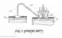
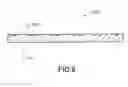
Referring to FIG. 1, according to a process for manufacturing a semiconductor package, the technology of wire bonding process widely applied to the electrical connection between a pad 11 of a chip 10 and a pad 13 of a substrate 12 by using a bonding wire 14. Wire bonding process is mainly based on gold (Au) wires, but copper (Cu) wire has an advantage of low cost. Compared with the gold, the copper has better electric conductivity and thermal conductivity, whereby the copper bonding wire has thinner diameter of wire and better dissipation of heat. However, the copper has disadvantage of insufficient ductility and easy oxidation such that the utilization of the copper bonding wire is restricted.
Recently, the copper bonding wire is only applied to a chip pad with a big size or low dielectric material (low-k) of wafer, because the success of the wire bonding process of the copper bonding wire depends on the structural strength of the chip pad. In order to avoid the failure of the wire bonding process of the copper bonding wire, the small size of the chip pad will be limited.
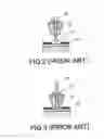
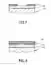
Referring to FIGS. 2 to 4, they depict a conventional method for bonding a copper bonding wire. Referring to FIG. 2, a copper bonding wire 20 is provided by a wire bonding machine, wherein the copper bonding wire 20 has a copper line 22 and a copper ball 24. The copper ball 24 is physically connected to an end of the copper line 22 by a discharging electricity manner or a burning hydrogen manner. Referring to FIG. 3, the copper ball 24 is pressed and then deformed. Referring to FIG. 4, the deformed copper ball 24 is bonded to an aluminum (Al) pad 32 by a vibration process. However, the prior art fails to disclose an additional adhesive force for enhancing the bond between a copper bonding wire and an aluminum pad.
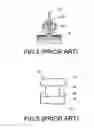
U.S. Pat. No. 7,115,446 B2, entitled “Flip Chip Bonding Method For Enhancing Adhesion Force In Flip Chip Packaging Process And Metal Layer-built Structure Of Substrate For The Same”, discloses that a method for packaging flip chip and a substrate structure can enhance the bond between a chip 50 and substrate 52 by forming bumps 54 on pads 51 of the chip 50 or pads 53 of the substrate 52.
Referring to FIG. 5, although an adhesive layer 56 disclosed in the U.S. Pat. No. 7,115,446 B2 can enhance the adhesive force during the bonding processes of flip chip, the adhesive layer 56 is not applied to the bonding process of the bonding wire. Furthermore, the adhesive layer 56 does not seal the whole bump 54, and thus the adhesive layer 56 cannot generate the effect upon mold lock.
Accordingly, there exists a need for a method for enhancing the bond of a bonding wire capable of solving the above-mentioned problems.
SUMMARY OF THE INVENTION
The present invention provides a wire bonding structure of a semiconductor package includes a bonding wire, a pad and a non-conductive adhesive material. The bonding wire includes a line portion and a block portion, wherein the block portion is physically connected to the line portion, and the sectional area of the block portion is bigger than that of the line portion. The pad is bonded to the block portion. The non-conductive adhesive material covers the pad and seals the whole block portion of the bonding wire.
According to the wire bonding structure of the present invention, the non-conductive adhesive material covers the aluminum pad and seals the whole block portion of the copper bonding wire, thereby enhancing the bond between the copper bonding wire and the aluminum pad. Furthermore, according to the above-mentioned wire bonding structure of the present invention, the non-conductive adhesive material covers the aluminum pad and seals the whole block portion of the copper bonding wire, thereby generating the effect upon mold lock. In addition, the non-conductive adhesive material covers the aluminum pad and seals the whole block portion of the copper bonding wire, thereby preventing the copper bonding wire from oxidation and electric leakage so as to cause the aluminum pads to have fine pitch.
The foregoing, as well as additional objects, features and advantages of the invention will be more apparent from the following detailed description, which proceeds with reference to the accompanying drawings.
BRIEF DESCRIPTION OF THE DRAWINGS
FIG. 1 is a cross-sectional view showing a method for bonding a wire in the prior art.
FIGS. 2 to 4 are cross-sectional views showing a method for bonding a copper bonding wire in the prior art.
FIG. 5 is a cross-sectional view showing a method for bonding flip chip in the prior art.
FIGS. 6 and 16 are cross-sectional views showing a method for manufacturing a semiconductor package according to the first embodiment of the present invention.
FIGS. 17 and 18 are cross-sectional views showing a method for enhancing the bond of a bonding wire according to the second embodiment of the present invention.
DETAILED DESCRIPTION OF THE PREFERRED EMBODIMENT
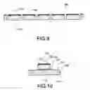
Referring to FIGS. 6 to 17, they depict a method for manufacturing a semiconductor package according to the first embodiment of the present invention. Referring to FIG. 6, a wafer 100 is provided, wherein the wafer 100 defines a plurality of chips 110 arranged in array manner. Referring to FIG. 7, it depicts a partially expanded cross-section of the chip 110. Each chip 110 includes a passivating layer 112 and at least one pad (e.g. aluminum pad 132). The aluminum pad 132 is electrically connected to the circuit of the chip 110. The passivating layer 112 covers the aluminum pad 132 and exposes a part of the aluminum pad 132. Referring to FIG. 8, a non-conductive adhesive material 140 is formed on the aluminum pad 132. The forming step of the non-conductive adhesive material 140 can include the following steps: the non-conductive adhesive material 140 is formed on the aluminum pad 132 by a spin coating process, and then the non-conductive adhesive material 140 is solidified from a liquid state to a half-solid state. Or, the forming step of the non-conductive adhesive material 140 can include the following steps: the non-conductive adhesive material 140 is formed on the aluminum pad 132 by a printing process, and then the non-conductive adhesive material 140 (e.g. typical adhesive) is solidified from a liquid state to a half-solid state. Or, the forming step of the non-conductive adhesive material 140 can include the following step: the non-conductive adhesive material 140 which is in a half-solid state is directly disposed on the aluminum pad 132.
Referring to FIG. 9, the wafer 100 is sawed to a plurality of chips 110 so as to form the chips 110 having the aluminum pad 132 and the non-conductive adhesive material 140 of the present invention. Referring to FIG. 10, the chip 110 is mounted on a carrier 106 by an adhesive 104. The carrier 106 can be a substrate or a leadframe. The carrier 106 has an upper surface 113 and a lower surface 114 opposite to the upper surface 113. A chip 110 is disposed on the carrier 106, wherein the chip 110 has an active surface 115 and a back surface 116 opposite to the active surface 115, and the back surface 116 of the chip 110 is located on the upper surface 113 of the carrier 106. The aluminum pad 132 is disposed on the active surface 215 of the chip 110.
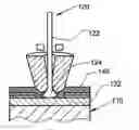
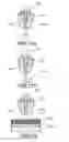
Referring to FIGS. 11a and 11b, a bonding wire (e.g. copper bonding wire 120) is provided by a wire bonding machine 102, wherein the copper bonding wire 120 has a line portion 122 and a block portion 124, wherein the block portion 124 is physically connected to an end of the line portion 122, and the cross-sectional area of the block portion 124 is bigger than that of the line portion 122. The block portion 124 can be spherical or non-spherical.
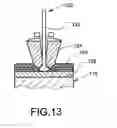
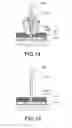
Referring to FIG. 12, the whole block portion 124 of the copper bonding wire 120 is inserted into the non-conductive adhesive material 140. Referring to FIG. 13, the block portion 124 is moved for contacting the aluminum pad 132, and is pressed and deformed by a pressing process. Referring to FIG. 14, the block portion 124 of the copper bonding wire 120 is bonded to the aluminum pad 132 by a vibration process, wherein the non-conductive adhesive material 140 covers the aluminum pad 132 and seals the whole block portion 124 of the copper bonding wire 120. Referring to FIG. 15, the non-conductive adhesive material 140 is solidified from a half-solid state to a solid state so as to form a wire bonding structure and a method for enhancing the bond of a bonding wire of the present invention.
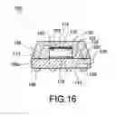
Referring to FIG. 16, the carrier 106 can be a substrate 106a, one end 125 of the copper bonding wire 120 is electrically connected to the aluminum pad 132, the other end 126 of the copper bonding wire 120 can be electrically connected to a pad 107 of the carrier 106. The substrate 106a includes external electrical contacts 146 located on the second surface 114.
Referring to FIG. 16 again, finally the chip 110 and the copper bonding wire 120 are sealed, and the carrier 106 is covered by a molding compound 138 so as to form a package, i.e. a semiconductor package 150 of the present invention, thereby finishing the method for manufacturing a semiconductor package of the present invention.
According to the wire bonding structure of the present invention, the non-conductive adhesive material covers the aluminum pad and seals the whole block portion of the copper bonding wire, thereby enhancing the bond between the copper bonding wire and the aluminum pad. Furthermore, according to the above-mentioned wire bonding structure of the present invention, the non-conductive adhesive material covers the aluminum pad and seals the whole block portion of the copper bonding wire, thereby generating the effect upon mold lock. In addition, the non-conductive adhesive material covers the aluminum pad and seals the whole block portion of the copper bonding wire, thereby preventing the copper bonding wire from oxidation and electric leakage so as to cause the aluminum pads to have fine pitch.
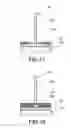
Referring to FIGS. 17 to 18, they depict a method for manufacturing a semiconductor package according to the second embodiment of the present invention. The method for manufacturing a semiconductor package according to the second embodiment is substantially similar to the method for manufacturing a semiconductor package according to the first embodiment, wherein the same elements are designated with the same reference numerals. The difference between the first and second embodiments is that the method for enhancing the bond of a bonding wire in the second embodiment includes the following steps. Referring to FIG. 17, the block portion 124 of the copper bonding wire 120 is firstly bonded to the aluminum pad 132. Referring to FIG. 18, then the aluminum pad 132 is covered by a non-conductive adhesive material 140′, and the whole block portion 124 of the copper bonding wire 120 is sealed by the non-conductive adhesive material 140′. Finally, the non-conductive adhesive material 140′ is solidified from a liquid state to a sold state so as to form a wire bonding structure of the present invention.
According to the wire bonding structure of the present invention, the non-conductive adhesive material covers the aluminum pad and seals the whole block portion of the copper bonding wire, thereby enhancing the bond between the copper bonding wire and the aluminum pad. Furthermore, according to the above-mentioned wire bonding structure of the present invention, the non-conductive adhesive material covers the aluminum pad and seals the whole block portion of the copper bonding wire, thereby generating the effect upon mold lock. In addition, the non-conductive adhesive material covers the aluminum pad and seals the whole block portion of the copper bonding wire, thereby preventing the copper bonding wire from oxidation and electric leakage so as to cause the aluminum pads to have fine pitch.
Although the invention has been explained in relation to its preferred embodiment, it is not used to limit the invention. It is to be understood that many other possible modifications and variations can be made by those skilled in the art without departing from the spirit and scope of the invention as hereinafter claimed.
Claims
What is claimed is:1. A semiconductor package comprising:
a carrier;
a chip disposed on the carrier, wherein the chip has a first surface and a second surface opposite to the active surface, and the chip comprises a pad disposed on the first surface.
a bonding wire for electrically connecting the chip to the carrier, wherein the bonding wire comprises a line portion and a block portion, the block portion is physically connected to the line portion, the sectional area of the block portion is bigger than that of the line portion, and the block portion is bonded to the pad;
a non-conductive adhesive material covering the pad and sealing the whole block portion of the bonding wire; and
a molding compound for sealing the chip and the bonding wire and covering the carrier.
2. The semiconductor package as claimed in claim 1, wherein the block portion is one of spherical and non-spherical block portion.
3. The semiconductor package as claimed in claim 1, wherein the bonding wire is a copper bonding wire.
4. The semiconductor package as claimed in claim 1, wherein the pad is an aluminum pad.
5. The semiconductor package as claimed in claim 1, wherein the pad of the chip is electrically connected to one end of the bonding wire, and the carrier includes another pad electrically connected to the other end of the bonding wire.
6. The semiconductor package as claimed in claim 1, wherein the carrier has an upper surface and a lower surface opposite to the upper surface, and the second surface of the chip is located on the upper surface of the carrier.
7. A method for manufacturing a semiconductor package comprising the following steps of:
providing a wafer, wherein the wafer defines a plurality of chips arranged in array manner, and each chip includes at least one pad;
forming a non-conductive adhesive material on the pad;
sawing the wafer so as to form the chips;
mounting the chip on a carrier;
providing a bonding wire comprising a line portion and a block portion, wherein the block portion is physically connected to the line portion, and the sectional area of the block portion is bigger than that of the line portion;
inserting the whole block portion of the copper bonding wire into the non-conductive adhesive material;
electrically connecting the chip to the carrier by the bonding wire, wherein the block portion of the bonding wire is boned to the pad, and the non-conductive adhesive material covers the pad and seals the whole block portion of the bonding wire;
solidifying the non-conductive adhesive material from a half-solid state to a solid state; and
sealing the chip and the bonding wire and covering the carrier by a molding compound, so as to form a package.
8. The method as claimed in claim 7, wherein the forming step of the non-conductive adhesive material on the pad comprises the following step:
forming the non-conductive adhesive material on the pad by a spin coating process.
9. The method as claimed in claim 8, wherein the forming step of the non-conductive adhesive material on the pad further comprises the following step:
solidifying the non-conductive adhesive material from a liquid state to a half-solid state.
10. The method as claimed in claim 7, wherein the forming step of the non-conductive adhesive material on the pad comprises the following step:
forming the non-conductive adhesive material on the pad by a printing process.
11. The method as claimed in claim 10, wherein the forming step of the non-conductive adhesive material on the pad further comprises the following step:
solidifying the non-conductive adhesive material from a liquid state to a half-solid state.
12. The method as claimed in claim 7, wherein the forming step of the non-conductive adhesive material on the pad comprises the following step:
solidifying the non-conductive adhesive material from a half-solid state to a solid state.
13. The method as claimed in claim 7, wherein the block portion is one of spherical and non-spherical block portion.
14. The method as claimed in claim 7, wherein the bonding wire is a copper bonding wire.
15. The method as claimed in claim 7, wherein the pad is an aluminum pad.
16. A method for manufacturing a semiconductor package comprising the following steps of:
providing a wafer, wherein the wafer defines a plurality of chips arranged in array manner, and each chip includes at least one pad;
sawing the wafer so as to form the chips;
mounting the chip on a carrier;
providing a bonding wire comprising a line portion and a block portion, wherein the block portion is physically connected to the line portion, and the sectional area of the block portion is bigger than that of the line portion;
electrically connecting the chip to the carrier by the bonding wire, wherein the block portion of the bonding wire is boned to the pad;
forming a non-conductive adhesive material on the pad, wherein the non-conductive adhesive material covers the pad and seals the whole block portion of the bonding wire;
solidifying the non-conductive adhesive material from a liquid state to a solid state; and
sealing the chip and the bonding wire and covering the carrier by a molding compound, so as to form a package.
17. The method as claimed in claim 16, wherein the forming step of the non-conductive adhesive material on the pad comprises the following step:
solidifying the non-conductive adhesive material from a half-solid state to a solid state.
18. The method as claimed in claim 16, wherein the block portion is one of spherical and non-spherical block portion.
19. The method as claimed in claim 16, wherein the bonding wire is a copper bonding wire.
20. The method as claimed in claim 16, wherein the pad is an aluminum pad.
Images & Drawings included:
Sources:
- United States Patent and Trademark Office - verify current appl. status at the USPTO↗
Recent applications in this class:
- » 20250266392 2025-08-21
Semiconductor packaging method and semiconductor packaging structure - » 20250239567 2025-07-24
METHODS OF FORMING WIRE INTERCONNECT STRUCTURES AND RELATED WIRE BONDING TOOLS - » 20250201765 2025-06-19
METHODS OF OPERATING WIRE BONDING SYSTEMS, INCLUDING METHODS OF DETECTING AND/OR PREVENTING WIRE FLY-OUT ON SUCH SYSTEMS - » 20250192098 2025-06-12
SEMICONDUCTOR APPARATUS AND METHOD FOR MANUFACTURING THE SAME, AND POWER CONVERSION APPARATUS - » 20250149502 2025-05-08
CAPILLARY FOR A WIRE BONDING MACHINE HAVING A DYNAMICALLY ADJUSTABLE CHAMFER DIAMETER - » 20250140740 2025-05-01
METHOD OF MANUFACTURING SEMICONDUCTOR DEVICE - » 20250140739 2025-05-01
LASER ENHANCED WIRE BONDING FOR SEMICONDUCTOR DEVICE PACKAGES - » 20250125305 2025-04-17
METHOD OF MANUFACTURING SEMICONDUCTOR DEVICE WITH FIXING FEATURE ON WHICH BONDING WIRE IS DISPOSED - » 20250118705 2025-04-10
PACKAGE-ON-PACKAGE ASSEMBLY WITH WIRE BOND VIAS - » 20250118704 2025-04-10
APPARATUS AND METHODS FOR TOOL MARK FREE STITCH BONDING
Recent applications for this Assignee:
- » 20250294670 2025-09-18
ELECTRONIC DEVICE - » 20250293221 2025-09-18
ELECTRONIC DEVICE - » 20250285950 2025-09-11
SEMICONDUCTOR DEVICE PACKAGE - » 20250282612 2025-09-11
PACKAGE STRUCTURE - » 20250273638 2025-08-28
SEMICONDUCTOR DEVICE PACKAGE INCLUDING STRESS BUFFERING LAYER - » 20250273531 2025-08-28
PACKAGE STRUCTURE - » 20250271555 2025-08-28
OPTOELECTRONIC STRUCTURE - » 20250266313 2025-08-21
SEMICONDUCTOR DEVICE PACKAGE AND METHOD OF MANUFACTURING THE SAME - » 20250260153 2025-08-14
ELECTRONIC DEVICE - » 20250259978 2025-08-14
SEMICONDUCTOR PACKAGE DEVICE AND METHOD OF MANUFACTURING THE SAME