Flexible light source device and fabrication method thereof
US20100163897A1
2010-07-01
12/422,291
2009-04-13
✅ Patent granted
US 7,763,895 B2
2010-07-27
-
-
Trung Dang
2029-04-13
Abstract:
A flexible light source device including a substrate, a light emitting device, a molding compound, a dielectric layer, and a metal line is provided. The substrate has a first surface, a second surface opposite to the first surface, and a first opening. The light emitting device is disposed on the first surface of the substrate and covers the first opening. The molding compound is located above the first surface and covers the light emitting device. The dielectric layer is disposed on the second surface and covers a sidewall of the first opening. The dielectric layer has a second opening which exposes part of the light emitting device. The metal line is disposed on the dielectric layer, wherein the metal line is electrically connected to the light emitting device via the second opening in the dielectric layer. Additionally, a fabrication method of the flexible light source device is also provided.
Inventors:
- Chao-Kai Hsu 7 🇹🇼 Hsinchu County, Taiwan
- Yu-Hua Chen 8 🇹🇼 Nantou County, Taiwan
- Zhi-Cheng Hsiao 3 🇹🇼 Hsinchu County, Taiwan
Assignee:
- INDUSTRIAL TECHNOLOGY RESEARCH INSTITUTE 7,890 🇹🇼 HSINCHU, Taiwan
Interested in similar patents?
Get notified when new applications in this technology area are published.
Classification:
H05K3/32 » CPC main
Apparatus or processes for manufacturing printed circuits; Assembling printed circuits with electric components, e.g. with resistor electrically connecting electric components or wires to printed circuits
H05K3/32 » CPC main
Apparatus or processes for manufacturing printed circuits; Assembling printed circuits with electric components, e.g. with resistor electrically connecting electric components or wires to printed circuits
H05K1/0274 » CPC further
Printed circuits; Details Optical details, e.g. printed circuits comprising integral optical means
H05K1/0274 » CPC further
Printed circuits; Details Optical details, e.g. printed circuits comprising integral optical means
H01L33/62 » CPC further
Semiconductor devices with at least one potential-jump barrier or surface barrier specially adapted for light emission; Processes or apparatus specially adapted for the manufacture or treatment thereof or of parts thereof; Details thereof characterised by the semiconductor body packages Arrangements for conducting electric current to or from the semiconductor body, e.g. lead-frames, wire-bonds or solder balls
H05K1/0203 » CPC further
Printed circuits; Details; Thermal arrangements, e.g. for cooling, heating or preventing overheating Cooling of mounted components
H05K1/0203 » CPC further
Printed circuits; Details; Thermal arrangements, e.g. for cooling, heating or preventing overheating Cooling of mounted components
H05K1/189 » CPC further
Printed circuits; Printed circuits structurally associated with non-printed electric components characterised by the use of a flexible or folded printed circuit
H05K1/189 » CPC further
Printed circuits; Printed circuits structurally associated with non-printed electric components characterised by the use of a flexible or folded printed circuit
H05K3/284 » CPC further
Apparatus or processes for manufacturing printed circuits; Secondary treatment of printed circuits; Applying non-metallic protective coatings for encapsulating mounted components
H05K3/284 » CPC further
Apparatus or processes for manufacturing printed circuits; Secondary treatment of printed circuits; Applying non-metallic protective coatings for encapsulating mounted components
H05K2201/09481 » CPC further
Indexing scheme relating to printed circuits covered by; Shape and layout; Shape and layout details of conductors; Pads and lands Via in pad; Pad over filled via
H05K2201/09481 » CPC further
Indexing scheme relating to printed circuits covered by; Shape and layout; Shape and layout details of conductors; Pads and lands Via in pad; Pad over filled via
H05K2201/0969 » CPC further
Indexing scheme relating to printed circuits covered by; Shape and layout; Shape and layout details of conductors covering at least two types of conductors provided for in - Apertured conductors
H05K2201/0969 » CPC further
Indexing scheme relating to printed circuits covered by; Shape and layout; Shape and layout details of conductors covering at least two types of conductors provided for in - Apertured conductors
H05K2201/10106 » CPC further
Indexing scheme relating to printed circuits covered by; Details of components or other objects attached to or integrated in a printed circuit board; Types of components Light emitting diode [LED]
H05K2201/10106 » CPC further
Indexing scheme relating to printed circuits covered by; Details of components or other objects attached to or integrated in a printed circuit board; Types of components Light emitting diode [LED]
H05K2201/2054 » CPC further
Indexing scheme relating to printed circuits covered by; Details of printed circuits not provided for in - Light-reflecting surface, e.g. conductors, substrates, coatings, dielectrics
H05K2201/2054 » CPC further
Indexing scheme relating to printed circuits covered by; Details of printed circuits not provided for in - Light-reflecting surface, e.g. conductors, substrates, coatings, dielectrics
H05K2203/1316 » CPC further
Indexing scheme relating to apparatus or processes for manufacturing printed circuits covered by; Moulding and encapsulation; Deposition techniques; Protective layers; Moulding and encapsulation Moulded encapsulation of mounted components
H05K2203/1316 » CPC further
Indexing scheme relating to apparatus or processes for manufacturing printed circuits covered by; Moulding and encapsulation; Deposition techniques; Protective layers; Moulding and encapsulation Moulded encapsulation of mounted components
H05K2203/1469 » CPC further
Indexing scheme relating to apparatus or processes for manufacturing printed circuits covered by; Related to the order of processing steps; Applying or finishing the circuit pattern after another process, e.g. after filling of vias with conductive paste, after making printed resistors Circuit made after mounting or encapsulation of the components
H01L2924/0002 » CPC further
Indexing scheme for arrangements or methods for connecting or disconnecting semiconductor or solid-state bodies as covered by; Technical content checked by a classifier Not covered by any one of groups , and
H01L2924/00 » CPC further
Indexing scheme for arrangements or methods for connecting or disconnecting semiconductor or solid-state bodies as covered by
H01L33/00 IPC
Semiconductor devices with at least one potential-jump barrier or surface barrier specially adapted for light emission; Processes or apparatus specially adapted for the manufacture or treatment thereof or of parts thereof; Details thereof
H01L29/267 IPC
Semiconductor devices adapted for rectifying, amplifying, oscillating or switching, or capacitors or resistors with at least one potential-jump barrier or surface barrier, e.g. PN junction depletion layer or carrier concentration layer; Details of semiconductor bodies or of electrodes thereof; Multistep manufacturing processes therefor; Semiconductor bodies ; Multistep manufacturing processes therefor characterised by the materials of which they are formed including, apart from doping materials or other impurities, elements provided for in two or more of the groups , , , , , e.g. alloys in different semiconductor regions, e.g. heterojunctions
Description
CROSS-REFERENCE TO RELATED APPLICATION
This application claims the priority benefit of Taiwan application serial no. 97151124, filed on Dec. 26, 2008. The entirety of the above-mentioned patent application is hereby incorporated by reference herein and made a part of specification.
BACKGROUND OF THE INVENTION
1. Field of the Invention
The present invention generally relates to a light source device and a fabrication method thereof, and more particularly, to a flexible light source device and a fabrication method thereof.
2. Description of Related Art
Solid state lighting (SSL) has many advantages such as small volume, high anti-shock ability, low power consumption, long lifespan, and high color diversity and purity, etc. Thereby, SSL has been broadly applied to various products. Because the designs of most application products are going towards high portability, those flexible products will certainly bring more convenience in their being carried around.
A SSL chip is a non-directional light source and accordingly the light output thereof is very limited. Besides, because the substrate therein absorbs light, the extraction efficiency of the entire SSL chip is reduced. Conventionally, the substrate is transposed or a reflective surface is coated over the substrate in order to prevent the substrate from absorbing light. However, the flexibility of the substrate will be reduced by aforementioned approaches. Besides, a large-sized high-power SSL may be adopted to improve the extraction efficiency thereof. Even though the large-sized SSL offers a higher light emitting efficiency, it produces more heat and accordingly the extraction efficiency thereof is reduced due to uneven current dispersion and heat accumulation.
SUMMARY OF THE INVENTION
The present invention provides a flexible light source device including a substrate, a light emitting device, a molding compound, a dielectric layer, and a metal line. The substrate has a first surface and a second surface opposite to the first surface, and the substrate has a first opening. The light emitting device is disposed on the first surface of the substrate and covers the first opening. The molding compound is located above the first surface of the substrate and covers the light emitting device. The dielectric layer is disposed on the second surface of the substrate and covers the sidewall of the first opening. It should be noted that the dielectric layer has a second opening which exposes part of the light emitting device. The metal line is disposed on the dielectric layer and is electrically connected to the light emitting device via the second opening in the dielectric layer.
The present invention also provides a fabrication method of a flexible light source device. The fabrication method includes following steps. First, a substrate is provided, wherein the substrate has a first surface and a second surface opposite to the first surface. Then, a light emitting device is disposed on the first surface of the substrate. Next, a molding compound is formed on the first surface of the substrate to cover the light emitting device. Thereafter, a first opening is formed on the second surface of the substrate, wherein the first opening exposes part of the light emitting device. Next, a dielectric layer is formed on the second surface of the substrate, and the dielectric layer is filled into the first opening. After that, a second opening is formed in the dielectric layer, and a metal line is formed on the dielectric layer, wherein the metal line is electrically connected to the light emitting device via the second opening.
As described above, in the present invention, a substrate and a molding compound are adopted in the flexible light source device and accordingly a high flexibility and a slim appearance of the flexible light source device are achieved.
BRIEF DESCRIPTION OF THE DRAWINGS
The accompanying drawings are included to provide a further understanding of the invention, and are incorporated in and constitute a part of this specification. The drawings illustrate embodiments of the invention and, together with the description, serve to explain the principles of the invention.
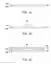
FIGS. 1A˜1I are flowcharts illustrating a fabrication method of a flexible light source device according to an embodiment of the present invention.
DESCRIPTION OF THE EMBODIMENTS
Reference will now be made in detail to the present preferred embodiments of the invention, examples of which are illustrated in the accompanying drawings. Wherever possible, the same reference numbers are used in the drawings and the description to refer to the same or like parts.
The present invention provides a flexible light source device having a high flexibility and a slim appearance. The present invention also provides a fabrication method for fabricating a flexible light source device having a high flexibility and a slim appearance.
FIGS. 1A˜1I are flowcharts illustrating a fabrication method of a flexible light source device according to an embodiment of the present invention. In the present embodiment, the fabrication method of the flexible light source device 100 includes following steps. First, referring to FIG. 1A, a substrate 110 is provided, wherein the substrate 110 has a first surface 110a and a second surface 110b opposite to the first surface 110a. Preferably, the substrate 110 is a flexible transparent substrate, and the flexible transparent substrate is made of a polymer material, such as polyimide (PI), polyurethane (PU), or silicon rubber, wherein the flexible radius of the flexible transparent substrate is greater than or equal to 5 cm.
Then, referring to FIG. 1B, a light emitting device 120 is disposed on the first surface 110a of the substrate 110. In an exemplary embodiment of the present invention, the light emitting device 120 may be a light emitting diode (LED) or other suitable light source. In addition, the light emitting device 120 may be disposed on the first surface 110a of the substrate 110 through a die bonding process or other suitable methods.
Next, referring to FIG. 1C, a molding compound 130 is formed on the first surface 110a of the substrate 110 to cover the light emitting device 120. The molding compound 130 is usually made of a material with its transmittance over 99%. In the present embodiment, the molding compound 130 may be silicone. In order to allow the light beams emitted by the light emitting device 120 to have a wider divergence angle, preferably, the molding compound 130 further contains optical diffusing particles 132 evenly distributed therein. To be specific, when a light beam emitted by the light emitting device 130 encounters the optical diffusing particles 132 evenly distributed in the molding compound 130, the light beam is refracted or dispersed so that it leaves its original path and is output from a different direction. As a result, the light beam emitted by the light emitting device 130 can irradiate a wider area and angle, and accordingly, a uniform light source can be provided.
After that, referring to FIG. 1D, a first opening 110c is formed on the second surface 110b of the substrate 110, wherein the first opening 110c exposes part of the light emitting device 120. In the present embodiment, the first opening 110c may be formed through laser drilling, etching, or other suitable methods.
In an exemplary embodiment of the present invention, in order to improve the extraction efficiency of the flexible light source device, a reflective film 140 may be further formed on the second surface 110b of the substrate 110, as shown in FIG. 1E. Namely, after the step illustrated in FIG. 1C, the reflective film 140 is first formed on the second surface 110b of the substrate 110, and then the first opening 110c is formed in both the substrate 110 and the reflective film 140. As a result, the structure illustrated in FIG. 1E is formed. The material of the reflective film 140 may be a metal layer, a reflective material stack layer, or other material with high reflectivity.
Thereafter, referring to FIG. IF, a dielectric layer 150 is formed on the second surface 110b of the substrate 110, and the dielectric layer 150 is filled into the first opening 110c. The dielectric layer 150 is mainly used for electrically separating the reflective film 140 and a subsequently formed metal line.
Next, referring to FIG. 1G, a second opening 150a is formed in the dielectric layer 150, and a metal line 160 is formed on the dielectric layer 150, wherein the metal line 160 is electrically connected to the light emitting device 120 via the second opening 150a. Due to the existence of the dielectric layer 150, short circuit between the metal line 160 and the reflective film 140 is prevented.
In an exemplary embodiment of the present invention, a heat conducting material 170 may be selectively attached above the second surface 110b of the substrate 110 in order to improve the performance in heat dissipation, wherein the heat conducting material 170 covers the metal line 160, as shown in FIG. 1H. The heat conducting material 170 can quickly disperse the heat produced during the operation of the light emitting device 120 so that the light emitting efficiency of the light emitting device 120 will not be reduced due to heat accumulation. The heat conducting material 170 may be made of a metal film or a polymer composite material.
Additionally, in order to improve the light mixing effect, an optical film set 180 may be further formed on the molding compound 130 after foregoing steps are completed, as shown in FIG. 11. The optical film set 180 may be a diffuser, a brightness enhancement film, a prism sheet, or a combination of foregoing elements. Preferably, the difference of refractive index between the molding compound 130 and the optical film set 180 is smaller than or equal to 0.3. In the present embodiment, the optical film set 180 may be directly attached to the surface of the molding compound 130 with an adhesive to achieve a no-gap tightly attached state between the optical film set 180 and the molding compound 130, so that a slim appearance and a brightness uniformity of over 80% of the flexible light source device 100 can be achieved.
It should be mentioned that in the embodiment described above, due to the existence of the optical diffusing particles 132 in the molding compound 130, a good dispersion or diffusion effect of the light beam emitted by the light emitting device 120 can be achieved when the light beam passes through the molding compound 130. Thus, in the present embodiment, the optical film set 180 can be directly attached to the surface of the molding compound 130 without having to be kept a certain distance away from the light emitting device 120 to achieve the uniform light emitting effect. Accordingly, the thickness of the flexible light source device 100 in the present embodiment is greatly reduced.
Only one light emitting device is illustrated as an example in the drawings of foregoing embodiment. Substantially, a plurality of light emitting devices 120 arranged in an array and metal lines 160 respectively disposed corresponding to the light emitting devices 120 are usually disposed on the substrate 110 to form a light source in a specific shape. However, the numbers of the light emitting devices and other elements are not limited in the present invention and which can be determined and adjusted according to the actual design.
Below, the structure of the flexible light source device fabricated through the fabrication method described above will be described in detail with reference to another embodiment of the present invention.
Referring to FIG. 11, in the present embodiment, the flexible light source device 100 includes a substrate 110, a light emitting device 120, a molding compound 130, a dielectric layer 150, and a metal line 160. The substrate 110 has a first surface 110a and a second surface 110b opposite to the first surface 110a, and the substrate 110 has a first opening 110c. The light emitting device 120 is disposed on the first surface 110a of the substrate 110 and covers the first opening 110c. The molding compound 130 is located above the first surface 110a of the substrate 110 and covers the light emitting device 120. The dielectric layer 150 is disposed on the second surface 110b of the substrate 110 and covers the sidewall of the first opening 110c. It should be noted that the dielectric layer 150 has a second opening 150a which exposes part of the light emitting device 120. Besides, the metal line 160 is disposed on the dielectric layer 150, and the metal line 160 is electrically connected to the light emitting device 120 via the second opening 150a in the dielectric layer 150.
In the present embodiment, the substrate 110 may be a flexible transparent substrate, and the flexible transparent substrate may be made of a polymer material, such as polyimide(PI), polyurethane(PU), or silicon rubber. Preferably, the flexible radius of the flexible transparent substrate is greater than or equal to 5 cm. The light emitting device 120 may be a LED or other suitable light source.
The molding compound 130 is used for protecting the light emitting device 120. Preferably, the transmittance of the molding compound 130 is over 99%. In the present embodiment, the molding compound 130 may further contain optical diffusing particles 132 evenly distributed therein. The optical diffusing particles 132 can effectively help the light beams emitted by the light emitting device 120 to form a uniform light source.
In order to improve the extraction efficiency of the flexible light source device 100, in the present embodiment, the flexible light source device 100 further includes a reflective film 140 disposed between the substrate 110 and the dielectric layer 150. The reflective film 140 may be made of a metal layer, a reflective material stack layer, or other material with high reflectivity.
In the present embodiment, the flexible light source device 100 further includes a heat conducting material 170 which is disposed above the second surface 110b of the substrate 110 and covers the metal line 160. The heat conducting material 170 improves the heat dissipation performance of the substrate 110 so that the light emitting efficiency of the light emitting device 120 will not be reduced due to heat accumulation. The heat conducting material 170 may be made of a metal film, a polymer composite material, or other material with high heat dissipation ability.
In the present embodiment, the flexible light source device 100 may further include an optical film set 180 disposed on the molding compound 130. The optical film set 180 may be directly attached to the molding compound 130 with an adhesive to achieve a no-gap bonding between the two. The optical film set 180 may be a diffuser, a brightness enhancement film, a prism sheet, or a combination of foregoing elements. Preferably, the difference of refractive index between the molding compound 130 and the optical film set 180 is smaller than or equal to 0.3.
Because the molding-compound 130 contains the optical diffusing particles 132 evenly distributed therein, the light beam emitted from the molding compound 130 presents a uniform state. Thus, the optical film set 180 may be directly attached to the molding compound 130 without being kept a certain distance away from the same. As a result, the flexible light source device 100 in the present embodiment can achieve a good light mixing effect without any light guide plate, and at the same time, a slim appearance thereof can be achieved.
As described above, in the present invention, a substrate and a molding compound are adopted such that the light emitting efficiency of the flexible light source device can be improved and a high flexibility and a slim appearance of the same can be achieved.
It will be apparent to those skilled in the art that various modifications and variations can be made to the structure of the present invention without departing from the scope or spirit of the invention. In view of the foregoing, it is intended that the present invention cover modifications and variations of this invention provided they fall within the scope of the following claims and their equivalents.
Claims
What is claimed is:1. A flexible light source device, comprising:
a substrate, having a first surface and a second surface opposite to the first surface, wherein the substrate has a first opening;
a light emitting device, disposed on the first surface of the substrate and covering the first opening;
a molding compound, located above the first surface of the substrate and covering the light emitting device;
a dielectric layer, disposed on the second surface of the substrate and covering a sidewall of the first opening, wherein the dielectric layer has a second opening which exposes a part of the light emitting device; and
a metal line, disposed on the dielectric layer, wherein the metal line is electrically connected to the light emitting device via the second opening in the dielectric layer.
2. The flexible light source device according to claim 1, wherein the molding compound comprises optical diffusing particles distributed therein.
3. The flexible light source device according to claim 1 further comprising a reflective film disposed between the substrate and the dielectric layer.
4. The flexible light source device according to claim 3, wherein the reflective film comprises a metal layer or a reflective material stack layer.
5. The flexible light source device according to claim 1 further comprising a heat conducting material which is disposed above the second surface of the substrate and covers the metal line.
6. The flexible light source device according to claim 5, wherein the heat conducting material comprises a metal film or a polymer composite material.
7. The flexible light source device according to claim 1 further comprising an optical film set disposed on the molding compound.
8. The flexible light source device according to claim 7, wherein the optical film set is directly attached to a surface of the molding compound.
9. The flexible light source device according to claim 7, wherein a difference of refractive index between the molding compound and the optical film set is smaller than or equal to 0.3.
10. The flexible light source device according to claim 7, wherein the optical film set comprises a diffuser, a brightness enhancement film, a prism sheet, or a combination thereof.
11. The flexible light source device according to claim 1, wherein the substrate is a flexible transparent substrate.
12. The flexible light source device according to claim 11, wherein a flexible radius of the flexible transparent substrate is greater than or equal to 5 cm.
13. The flexible light source device according to claim 11, wherein a material of the flexible transparent substrate is a polymer material.
14. The flexible light source device according to claim 1, wherein the light emitting device is a light emitting diode (LED).
15. A fabrication method of a flexible light source device, comprising:
providing a substrate, wherein the substrate has a first surface and a second surface opposite to the first surface;
disposing a light emitting device on the first surface of the substrate;
forming a molding compound on the first surface of the substrate to cover the light emitting device;
forming a first opening on the second surface of the substrate, wherein the first opening exposes a part of the light emitting device;
forming a dielectric layer on the second surface of the substrate, and filling the dielectric layer into the first opening;
forming a second opening in the dielectric layer; and
forming a metal line on the dielectric layer, wherein the metal line is electrically connected to the light emitting device via the second opening.
16. The fabrication method according to claim 15, wherein the molding compound further comprises optical diffusing particles distributed therein.
17. The fabrication method according to claim 15, wherein before forming the dielectric layer, the fabrication method further comprises:
forming a reflective film on the second surface of the substrate; and
forming the first opening in the substrate and the reflective film.
18. The fabrication method according to claim 15, wherein after forming the metal line on the dielectric layer, the fabrication method further comprises attaching a heat conducting material above the second surface of the substrate and covering the metal line.
19. The fabrication method according to claim 15 further comprising forming an optical film set on the molding compound.
20. The fabrication method according to claim 19, wherein the optical film set is directly attached to a surface of the molding compound.
21. The fabrication method according to claim 15, wherein the light emitting device is disposed on the first surface of the substrate through a die bonding process.
Images & Drawings included:


Sources:
- United States Patent and Trademark Office - verify current appl. status at the USPTO↗
Recent applications in this class:
- » 20250203784 2025-06-19
Sintering Methods - » 20250113443 2025-04-03
ELECTRONIC DEVICES, SOCKET LOADING MECHANISMS, AND METHODS - » 20250056734 2025-02-13
CONNECTION METHOD FOR YARN WIRE AND CIRCUIT BOARD - » 20240381540 2024-11-14
MANUFACTURING METHOD OF ELECTRONIC DEVICE - » 20240381539 2024-11-14
SINTERING PASTE, METHOD FOR ELECTRICALLY CONDUCTIVE, MATERIALLY BONDED CONNECTION OF AN ALUMINUM CONDUCTOR COVERED WITH AN OXIDE LAYER TO AN ELECTRONIC COMPONENT AND ELECTRONIC PRODUCT - » 20240314938 2024-09-19
Extension structure of flexible substrates with conductive wires thereon - » 20240306311 2024-09-12
Connection of Two Components with One Connecting Element - » 20240237226 2024-07-11
CLAMPING DEVICE WITH PIVOTING RETAINER - » 20240138073 2024-04-25
CLAMPING DEVICE WITH PIVOTING RETAINER - » 20230254981 2023-08-10
Bonding apparatus
Recent applications for this Assignee:
- » 20250289330 2025-09-18
MOBILE VEHICLE CHARGING PROTECTION DEVICE FOR ELECTRICAL SAFETY IN LIVESTOCK HOUSES - » 20250287224 2025-09-11
COMMUNICATION DEVICE AND COMMUNICATION METHOD - » 20250286593 2025-09-11
COMMUNICATION DEVICE AND METHOD OF BEAM MANAGEMENT - » 20250284336 2025-09-11
SYSTEM AND METHOD FOR ADJUSTING IMAGE BASED ON PHYSIOLOGICAL INFORMATION AND POSTURE - » 20250281908 2025-09-11
ELECTROCATALYST COMPOSITION AND PREPARATION METHOD THEREOF - » 20250273403 2025-08-28
CAPACITOR AND ELECTRONIC DEVICE - » 20250271759 2025-08-28
POLYMER, POSITIVE PHOTORESIST COMPOSITION, AND METHOD FOR FORMING PATTERNED PHOTORESIST LAYER - » 20250265803 2025-08-21
MULTI-SENSOR COORDINATION METHOD, PROCESSING DEVICE, AND INFORMATION DISPLAY SYSTEM - » 20250263659 2025-08-21
METHOD AND KIT FOR PREPARING AN IMMUNE CELL DIFFERENTIATED FROM A STEM CELL - » 20250252547 2025-08-07
CORROSION POSITIONING SYSTEM, CORROSION INSPECTION VEHICLE AND CORROSION POSITIONING METHOD USING THE SAME