PACKAGE DEVICE AND FABRICATION METHOD THEREOF
US20110204514A1
2011-08-25
12/815,087
2010-06-14
Abstract:
A package device and a fabrication method thereof comprises providing a plurality of package units each having a plurality of penetrated holes; stacking the plurality of package units in a manner such that the penetrated holes of the plurality of package units are aligned; filling a conductive material into the plurality of penetrated holes substantially, so as to electrically connect the plurality of package units through the conductive material; and disposing a plurality of solder balls on the bottom of the conductive material filling the plurality of penetrated holes, and connecting the plurality of solder balls with the conductive material electrically.
Interested in similar patents?
Get notified when new applications in this technology area are published.
Classification:
H01L2924/00012 » CPC further
Indexing scheme for arrangements or methods for connecting or disconnecting semiconductor or solid-state bodies as covered by; Technical content checked by a classifier Relevant to the scope of the group, the symbol of which is combined with the symbol of this group
H01L25/105 » CPC main
Assemblies consisting of a plurality of individual semiconductor or other solid state devices ; Multistep manufacturing processes thereof all the devices being of a type provided for in the same subgroup of groups - , e.g. assemblies of rectifier diodes the devices having separate containers the devices being of a type provided for in group
H01L24/16 » CPC further
Arrangements for connecting or disconnecting semiconductor or solid-state bodies; Methods or apparatus related thereto; Means for bonding being attached to, or being formed on, the surface to be connected, e.g. chip-to-package, die-attach, "first-level" interconnects; Manufacturing methods related thereto; Bump connectors ; Manufacturing methods related thereto; Structure, shape, material or disposition of the bump connectors after the connecting process of an individual bump connector
H01L24/48 » CPC further
Arrangements for connecting or disconnecting semiconductor or solid-state bodies; Methods or apparatus related thereto; Means for bonding being attached to, or being formed on, the surface to be connected, e.g. chip-to-package, die-attach, "first-level" interconnects; Manufacturing methods related thereto; Wire connectors; Manufacturing methods related thereto; Structure, shape, material or disposition of the wire connectors after the connecting process of an individual wire connector
H01L24/73 » CPC further
Arrangements for connecting or disconnecting semiconductor or solid-state bodies; Methods or apparatus related thereto Means for bonding being of different types provided for in two or more of groups , , , , , , ,
H01L2225/1023 » CPC further
Details relating to assemblies covered by the group but not provided for in its subgroups; All the devices being of a type provided for in the same subgroup of groups - the devices having separate containers the devices being of a type provided for in group the containers being in a stacked arrangement the lowermost container comprising a device support the support being an insulating substrate
H01L2225/1058 » CPC further
Details relating to assemblies covered by the group but not provided for in its subgroups; All the devices being of a type provided for in the same subgroup of groups - the devices having separate containers the devices being of a type provided for in group the containers being in a stacked arrangement; Details of electrical connections between containers Bump or bump-like electrical connections, e.g. balls, pillars, posts
H01L2924/01079 » CPC further
Indexing scheme for arrangements or methods for connecting or disconnecting semiconductor or solid-state bodies as covered by; Chemical elements Gold [Au]
H01L2924/15331 » CPC further
Indexing scheme for arrangements or methods for connecting or disconnecting semiconductor or solid-state bodies as covered by; Details of package parts other than the semiconductor or other solid state devices to be connected; Die mounting substrate; Connection portion the connection portion being formed on the die mounting surface of the substrate the connection portion being formed both on the die mounting surface of the substrate and outside the die mounting surface of the substrate being a ball array, e.g. BGA
H01L2224/45099 » CPC further
Indexing scheme for arrangements for connecting or disconnecting semiconductor or solid-state bodies and methods related thereto as covered by; Means for bonding being attached to, or being formed on, the surface to be connected, e.g. chip-to-package, die-attach, "first-level" interconnects; Manufacturing methods related thereto; Wire connectors; Manufacturing methods related thereto; Structure, shape, material or disposition of the wire connectors prior to the connecting process of an individual wire connector; Core members of the connector Material
H01L2924/00014 » CPC further
Indexing scheme for arrangements or methods for connecting or disconnecting semiconductor or solid-state bodies as covered by; Technical content checked by a classifier the subject-matter covered by the group, the symbol of which is combined with the symbol of this group, being disclosed without further technical details
H01L2924/15311 » CPC further
Indexing scheme for arrangements or methods for connecting or disconnecting semiconductor or solid-state bodies as covered by; Details of package parts other than the semiconductor or other solid state devices to be connected; Die mounting substrate; Connection portion the connection portion being formed only on the surface of the substrate opposite to the die mounting surface being a ball array, e.g. BGA
H01L2224/73265 » CPC further
Indexing scheme for arrangements for connecting or disconnecting semiconductor or solid-state bodies and methods related thereto as covered by; Means for bonding being of different types provided for in two or more of groups; Location after the connecting process on different surfaces Layer and wire connectors
H01L2924/00 » CPC further
Indexing scheme for arrangements or methods for connecting or disconnecting semiconductor or solid-state bodies as covered by
H01L2924/181 » CPC further
Indexing scheme for arrangements or methods for connecting or disconnecting semiconductor or solid-state bodies as covered by; Details of package parts other than the semiconductor or other solid state devices to be connected Encapsulation
H01L2924/207 » CPC further
Indexing scheme for arrangements or methods for connecting or disconnecting semiconductor or solid-state bodies as covered by; Parameters Diameter ranges
H01L23/498 IPC
Details of semiconductor or other solid state devices; Arrangements for conducting electric current to or from the solid state body in operation, e.g. leads, terminal arrangements ; Selection of materials therefor consisting of soldered constructions Leads, on insulating substrates,
H01L21/60 IPC
Processes or apparatus adapted for the manufacture or treatment of semiconductor or solid state devices or of parts thereof; Manufacture or treatment of semiconductor devices or of parts thereof the devices having at least one potential-jump barrier or surface barrier, e.g. PN junction, depletion layer or carrier concentration layer; Assembly of semiconductor devices using processes or apparatus not provided for in a single one of the subgroups - , e.g. sealing of a cap to a base of a container Attaching or detaching leads or other conductive members, to be used for carrying current to or from the device in operation
Description
BACKGROUND OF THE INVENTION
1. Field of the Invention
The present invention is related to a package device and the fabrication method thereof, and more particularly to a package device and the fabrication method thereof having a plurality of package units stacked.
2. Description of the Prior Art
The electronic products nowadays develop according to the trend toward a lighter, thinner, shorter and smaller device. However, when the functions of various electronic parts are growing with the demands of users, the number of pins of the semiconductor package device in electronic parts is also increasing. As a result, size reduction becomes a problem getting increasingly harder to solve. Therefore, vendors and R&D (research and development) personnel have been working hard to find various packaging technology to accommodate more semiconductor package devices under a constant area.
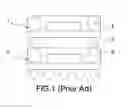
FIG. 1 is a schematic diagram illustrating a prior art stacked package units. As shown in the figure, two package units 1, 1′ are arranged to be stacked, and are electrically connected to each other through a plurality of solder balls 2. However, in the prior art technology, the solder ball 2 has a certain volume, and thus can cause the plurality of solder balls 2 to interfere with each other or to contact and short circuit. Besides, the overall height of the device would also be affected by the size of the solder ball 2. Therefore, it is highly desirable to provide a technology for stacking package units which avoids using solder balls to further reduce the overall height of the device.
SUMMARY OF THE INVENTION
In order to solve the aforementioned problem, the present invention provides a package device and the fabrication method thereof, which effectively integrates more package units without increasing the area for stacking, and eliminates the need to use solder balls for electrical connection between the package units to reduce the overall height of the device.
In order to achieve the aforementioned objects, one objective of the present invention is to provide a package device comprising a plurality of package units, a plurality of penetrated holes, a conductive material, and a plurality of solder balls. The plurality of package units are arranged to be stacked. The plurality of penetrated holes penetrate the stacked package units. The conductive material substantially fills the penetrated holes, and the stacked package units are electrically connected with each other through the conductive material. The plurality of solder balls are disposed on the bottom of penetrated holes and are electrically connected with the conductive material.
Another objective of the present invention is to provide a fabrication method of the package device comprising providing a plurality of package units, each having a plurality of penetrated holes; stacking the plurality of package units, wherein the plurality of package units are arranged to be stacked in a manner such that the penetrated holes of the plurality of package units are aligned; filling the plurality of penetrated holes with a conductive material substantially so that the plurality of package units are electrically connected through the conductive material; and disposing a plurality of solder balls on the bottom of the conductive material substantially filling the plurality of penetrated holes, so that the solder balls are electrically connected with the conductive material.
The objective, technologies, features and advantages of the present invention will become more apparent from the following description in conjunction with the accompanying drawings, wherein certain embodiments of the present invention are set forth by way of illustration and examples.
BRIEF DESCRIPTION OF THE DRAWINGS
FIG. 1 is schematic diagram illustrating a prior art stacked package units;
FIG. 2A to FIG. 2C are schematic diagrams illustrating the package device and the fabrication method thereof according to an embodiment of the present invention; and
FIG. 3 is a schematic structural diagram illustrating the package device according to an embodiment of the present invention.
DESCRIPTION OF THE PREFERRED EMBODIMENT
According to the present invention, the package device and the fabrication method thereof comprises providing a plurality of package units each having a plurality of penetrated holes; stacking the plurality of package units, wherein the plurality of package units are arranged to be stacked in a manner such that their penetrated holes are aligned; filling the plurality of penetrated holes with a conductive material substantially, so that the plurality of package units are electrically connected with each other through the conductive material; and disposing a plurality of solder balls on the bottom of the plurality of penetrated holes filled with the conductive material, and connecting the plurality of solder balls electrically with the conductive material.
For clarity of description, the embodiment of the package device and the fabrication method thereof disclosed below take two package units as an example. However, as persons skilled in the art may understand, the number of package units of the package device and the fabrication method thereof according to the present invention can be adjusted according to demand.
Referring to FIG. 2A to FIG. 2C, there are illustrated an embodiment of the package device and the fabrication method thereof. As shown in FIG. 2A, a first package unit 10 and a second package unit 20 are provided. The first package unit 10 and the second package unit 20 are of the same structure. The first package unit 10, taken as an example, comprises a substrate 11; at least one chip 12 disposed on the substrate 11, and electrically connected with the substrate 11 through flip chip bonding or wire bonding. The first package unit 10 can further comprise an encapsulation body 13 for encapsulating the substrate 11 and the chip 12 to a degree such that only the bottom of the substrate is exposed. In addition, the first package unit 10 and the second package unit 20 respectively have a plurality of first penetrated holes 14 and a plurality of second penetrated holes 24 respectively penetrating the first package unit 10 and the second package unit 20. For the first package unit 10, for example, the plurality of the first penetrated holes 14 penetrate the encapsulation body 13 and the substrate 11. Next, as shown in FIG. 2B, the second package unit 20 is stacked on the first package unit 10, i.e. the bottom (not indicated) of the substrate of the second package unit 20 is stacked on the encapsulation body 13 of the first package unit 10, and the plurality of second penetrated holes 24 are aligned with the plurality of first penetrated holes 14. As shown in FIG. 2C, the first penetrated holes 14 and the second penetrated holes 24 are substantially filled with a conductive material 30, so that the first package unit 10 and the second package unit 20 can connect to each other electrically through the conductive material 30, wherein the conductive material 30 can be metal such as gold, silver, nickel or copper. Next, a plurality of solder balls 15 are disposed on the bottom of the conductive material 30 substantially filling the first penetrated holes 14 and the second penetrated holes 24 so that the solder balls 15 are electrically connected with the conductive material 30.
It is noted that the method of filling the plurality of first penetrated holes 14 and the plurality of second penetrated holes 24 with the conductive material 30 may comprise heating the stacked first package unit 10 and the second package unit 20, and using a sputtering technology to sputter the conductive material into the plurality of first penetrated holes 14 and the plurality of second penetrated holes 24, wherein the heated first package unit 10 and the second package unit 20 cause the conductive material 30 to reflow in the plurality of first penetrated holes 14 and the plurality of second penetrated holes 24, thereby assuring the plurality of first penetrated holes 14 and the plurality of second penetrated holes 24 to be filled. Alternatively, the method of filling the plurality of first penetrated holes 14 and the plurality of second penetrated holes 24 with the conductive material 30 may comprise ionizing the conductive material 30 in a chamber, and then applying a negative potential to the stacked first package unit 10 and the second package unit 20 to attract the ionized conductive material 30 into the plurality of first penetrated holes 14 and the plurality of second penetrated holes 24, thereby assuring the plurality of the first penetrated holes 14 and the plurality of second penetrated holes 24 to be filled.
Through the aforementioned fabrication method, the present invention provides a package device as illustrated in FIG. 3. According to an embodiment illustrated in FIG. 3, the package device 100 comprises a first package unit 110, a second package unit 120, a conductive material 130, a plurality of penetrated holes 140, and a plurality of solder balls 150. As shown in the figure, the second package unit 120 is stacked on the first package unit 110. The plurality of penetrated holes 140 penetrate the first packaged unit 110 and the second package unit 120. The conductive material 130 substantially fills the plurality of penetrated holes 140 so that the first package unit 110 and the second package unit 120 are electrically connected with each other through the conductive material 130 in the plurality of penetrated holes 140. A plurality of solder balls 150 are disposed on the bottom of the conductive material 130 substantially filling the penetrated holes 140 and are connected electrically with the conductive material 130. The first package unit 110 and the second package unit 120 are of the same structure as the package unit mentioned above, and their description is therefore omitted here. Moreover, according to another embodiment, the package device 100 further comprises a plurality of adhesive layers (not indicated) disposed between the first package unit 110 and the second package unit 120, for fixing the stacked first package unit 110, and the second package unit 120.
In conclusion, the present invention provides a package device and the fabrication method thereof electrically connecting the package units with the conductive material filling the penetrated holes penetrating the stacked package units. In such way, not only does the present invention enable more package units be integrated effectively without increasing the area for stacking, but it also eliminates the need to use solder balls for electrical connection between the package units to decrease the overall height of the device.
While the invention is susceptible to various modifications and alternative forms, a specific example thereof has been shown in the drawings and is herein described in detail. It should be understood, however, that the invention is not to be limited to the particular form disclosed, but to the contrary, the invention is to cover all modifications, equivalents, and alternatives falling within the spirit and scope of the appended claims.
Claims
What is claimed is:1. A package device comprising:
a plurality of package units, each having a plurality of penetrated holes, wherein the plurality of package units are arranged to be stacked in a manner such that the penetrated holes of the plurality of package units are aligned;
a conductive material, substantially filling the plurality of penetrated holes, wherein the plurality of package units are electrically connected with each other through the conductive material; and
a plurality of solder balls, disposed on the bottom of the conductive material substantially filling the plurality of penetrated holes, and connected electrically with the conductive material.
2. The package device according to claim 1, wherein the conductive material comprises gold, silver, nickel or copper.
3. The package device according to claim 1, wherein each of the package units comprises:
a substrate, wherein the plurality of penetrated holes penetrate the substrate; and
at least one chip disposed on the substrate, and connected electrically with the substrate.
4. The package device according to claim 3, wherein each of the package units further comprises an encapsulation body for encapsulating the substrate and the chip to a degree such that only the bottom of the substrate is exposed, wherein the plurality of penetrated holes penetrate the encapsulation body.
5. The package device according to claim 4, wherein any two of the package units are arranged to be stacked in a manner such that the bottom of the substrate of the upper package unit is stacked on the encapsulation body of the lower package unit.
6. The package device according to claim 3, wherein each of the package units further comprises a plurality of solder balls or a plurality of bond wires, connecting the chip and the substrate electrically.
7. The package device according to claim 3, further comprising a plurality of adhesive layers disposed between the plurality of package units for fixing the stacked package units.
8. A fabrication method of a package device comprising:
providing a plurality of package units, wherein each of the package unit has a plurality of penetrated holes;
stacking the plurality of package units, wherein the plurality of package units are arranged to be stacked in a manner such that the penetrated holes of the plurality of package units are aligned;
filling the plurality of penetrated holes with a conductive material substantially so that the plurality of package units are electrically connected with each other through the conductive material; and
disposing a plurality of solder balls on the bottom of the conductive material substantially filling the plurality of penetrated holes, and connecting the plurality of solder balls electrically with the conductive material.
9. The fabrication method of a package unit according to claim 8, wherein the method of filling the conductive material in the plurality of penetrated holes comprises:
heating the stacked package units; and
using a sputtering technology to sputter the conductive material into the plurality of penetrated holes, wherein the heated package units causes the conductive material to reflow in the plurality of penetrated holes thereby filling the plurality of penetrated holes.
10. The fabrication method of a package unit according to claim 8, wherein the method for providing the conductive material filling the plurality of penetrated holes comprises:
ionizing the conductive material; and
applying a negative potential to the stacked package units so as to attract the ionized conductive material into the plurality of penetrated holes to fill the plurality of penetrated holes.
Images & Drawings included:


Sources:
- United States Patent and Trademark Office - verify current appl. status at the USPTO↗
Similar patent applications:
- » 20240332152
INTEGRATED PACKAGE DEVICE, FABRICATION METHOD THEREOF AND MEMORY SYSTEM - » 20210280563
SEMICONDUCTOR DEVICE, FABRICATION METHOD THEREOF, PACKAGE AND FABRICATION METHOD THEREOF - » 20160056381
Electronic package device for testing a package effect of the device, fabrication method thereof and method for testing electronic package device - » 20120133048
Semiconductor device, fabricating method thereof and semiconductor package including the semiconductor device - » 20090289318
Electronics device package and fabrication method thereof - » 20110181182
TOP VIEW LIGHT EMITTING DEVICE PACKAGE AND FABRICATION METHOD THEREOF - » 20110233782
Electronic device package and fabrication method thereof - » 20090289345
Electronic device package and fabrication method thereof - » 20100171189
Electronic device package and fabrication method thereof - » 20090020881
Semiconductor device package and fabricating method thereof
Recent applications in this class:
- » 20250174609 2025-05-29
PACKAGE STRUCTURE AND MANUFACTURING METHOD THEREOF - » 20250167183 2025-05-22
FAN OUT PACKAGING POP MECHANICAL ATTACH METHOD - » 20250157997 2025-05-15
VERTICAL SEMICONDUCTOR PACKAGE INCLUDING HORIZONTALLY STACKED DIES AND METHODS OF FORMING THE SAME - » 20250157996 2025-05-15
SEMICONDUCTOR PACKAGES - » 20250149517 2025-05-08
TILED DISPLAY DEVICE - » 20250149516 2025-05-08
SEMICONDUCTOR PACKAGE - » 20250149515 2025-05-08
SEMICONDUCTOR PACKAGES - » 20250149514 2025-05-08
PACKAGE ON PACKAGE SEMICONDUCTOR DEVICE WITH INTEGRATED WAVEGUIDE AND METHOD THEREFOR - » 20250132296 2025-04-24
SEMICONDUCTOR PACKAGE AND MANUFACTURING METHOD THEREOF - » 20250125317 2025-04-17
SEMICONDUCTOR PACKAGE AND STACKED PACKAGE MODULE INCLUDING THE SAME