Electronic device package and fabrication method thereof
US20100171189A1
2010-07-08
12/652,715
2010-01-05
✅ Patent granted
US 9,181,084 B2
2015-11-10
-
-
Laura Menz | Candice Y Chan
Liu & Liu
2032-04-21
Abstract:
The invention provides an electronic device package and fabrication method thereof. The electronic device package includes a sensor chip. An upper surface of the sensor chip comprises a sensing film. A covering plate having an opening structure covers the upper surface of the sensor chip. A cavity is between the covering plate and the sensor chip, corresponding to a position of the sensing film, where the cavity communicates with the opening structure. A spacer is between the covering plate and the sensor chip, surrounding the cavity. A pressure releasing region is between the spacer and the sensing film.
Applicant:
Interested in similar patents?
Get notified when new applications in this technology area are published.
Classification:
B81C1/00325 » CPC main
Manufacture or treatment of devices or systems in or on a substrate for manufacturing microsystems; Processes for packaging MEMS devices for reducing stress inside of the package structure
B81C2201/0115 » CPC further
Manufacture or treatment of microstructural devices or systems in or on a substrate; Shaping material; Structuring the bulk substrate or layers on the substrate; Film patterning; Bulk micromachining Porous silicon
H01L2224/0231 » CPC further
Indexing scheme for arrangements for connecting or disconnecting semiconductor or solid-state bodies and methods related thereto as covered by; Means for bonding being attached to, or being formed on, the surface to be connected, e.g. chip-to-package, die-attach, "first-level" interconnects; Manufacturing methods related thereto; Bonding areas; Manufacturing methods related thereto; Redistribution layers [RDL] for bonding areas Manufacturing methods of the redistribution layers
H01L2224/11 » CPC further
Indexing scheme for arrangements for connecting or disconnecting semiconductor or solid-state bodies and methods related thereto as covered by; Means for bonding being attached to, or being formed on, the surface to be connected, e.g. chip-to-package, die-attach, "first-level" interconnects; Manufacturing methods related thereto; Bump connectors; Manufacturing methods related thereto Manufacturing methods
H01L2224/13099 » CPC further
Indexing scheme for arrangements for connecting or disconnecting semiconductor or solid-state bodies and methods related thereto as covered by; Means for bonding being attached to, or being formed on, the surface to be connected, e.g. chip-to-package, die-attach, "first-level" interconnects; Manufacturing methods related thereto; Bump connectors; Manufacturing methods related thereto; Structure, shape, material or disposition of the bump connectors prior to the connecting process of an individual bump connector; Core members of the bump connector Material
H01L21/6835 » CPC further
Processes or apparatus adapted for the manufacture or treatment of semiconductor or solid state devices or of parts thereof; Apparatus specially adapted for handling semiconductor or electric solid state devices during manufacture or treatment thereof; Apparatus specially adapted for handling wafers during manufacture or treatment of semiconductor or electric solid state devices or components ; Apparatus not specifically provided for elsewhere for supporting or gripping using temporarily an auxiliary support
H01L2924/15788 » CPC further
Indexing scheme for arrangements or methods for connecting or disconnecting semiconductor or solid-state bodies as covered by; Details of package parts other than the semiconductor or other solid state devices to be connected; Die mounting substrate; Material with a principal constituent of the material being a non metallic, non metalloid inorganic material Glasses, e.g. amorphous oxides, nitrides or fluorides
H01L2924/00 » CPC further
Indexing scheme for arrangements or methods for connecting or disconnecting semiconductor or solid-state bodies as covered by
H01L29/84 IPC
Semiconductor devices adapted for rectifying, amplifying, oscillating or switching, or capacitors or resistors with at least one potential-jump barrier or surface barrier, e.g. PN junction depletion layer or carrier concentration layer; Details of semiconductor bodies or of electrodes thereof; Multistep manufacturing processes therefor; Types of semiconductor device ; Multistep manufacturing processes therefor controllable by variation of applied mechanical force, e.g. of pressure
H01L21/50 IPC
Processes or apparatus adapted for the manufacture or treatment of semiconductor or solid state devices or of parts thereof; Manufacture or treatment of semiconductor devices or of parts thereof the devices having at least one potential-jump barrier or surface barrier, e.g. PN junction, depletion layer or carrier concentration layer Assembly of semiconductor devices using processes or apparatus not provided for in a single one of the subgroups - , e.g. sealing of a cap to a base of a container
B81B2207/092 » CPC further
Microstructural systems or auxiliary parts thereof; Packages; Arrangements for connecting external electrical signals to mechanical structures inside the package Buried interconnects in the substrate or in the lid
B81B2207/097 » CPC further
Microstructural systems or auxiliary parts thereof; Packages; Arrangements for connecting external electrical signals to mechanical structures inside the package Interconnects arranged on the substrate or the lid, and covered by the package seal
B81C2203/0118 » CPC further
Forming microstructural systems; Packaging MEMS Bonding a wafer on the substrate, i.e. where the cap consists of another wafer
H01L24/11 » CPC further
Arrangements for connecting or disconnecting semiconductor or solid-state bodies; Methods or apparatus related thereto; Means for bonding being attached to, or being formed on, the surface to be connected, e.g. chip-to-package, die-attach, "first-level" interconnects; Manufacturing methods related thereto; Bump connectors ; Manufacturing methods related thereto Manufacturing methods
H01L24/13 » CPC further
Arrangements for connecting or disconnecting semiconductor or solid-state bodies; Methods or apparatus related thereto; Means for bonding being attached to, or being formed on, the surface to be connected, e.g. chip-to-package, die-attach, "first-level" interconnects; Manufacturing methods related thereto; Bump connectors ; Manufacturing methods related thereto; Structure, shape, material or disposition of the bump connectors prior to the connecting process of an individual bump connector
H01L24/29 » CPC further
Arrangements for connecting or disconnecting semiconductor or solid-state bodies; Methods or apparatus related thereto; Means for bonding being attached to, or being formed on, the surface to be connected, e.g. chip-to-package, die-attach, "first-level" interconnects; Manufacturing methods related thereto; Layer connectors, e.g. plate connectors, solder or adhesive layers; Manufacturing methods related thereto; Structure, shape, material or disposition of the layer connectors prior to the connecting process of an individual layer connector
H01L24/32 » CPC further
Arrangements for connecting or disconnecting semiconductor or solid-state bodies; Methods or apparatus related thereto; Means for bonding being attached to, or being formed on, the surface to be connected, e.g. chip-to-package, die-attach, "first-level" interconnects; Manufacturing methods related thereto; Layer connectors, e.g. plate connectors, solder or adhesive layers; Manufacturing methods related thereto; Structure, shape, material or disposition of the layer connectors after the connecting process of an individual layer connector
H01L24/83 » CPC further
Arrangements for connecting or disconnecting semiconductor or solid-state bodies; Methods or apparatus related thereto; Methods for connecting semiconductor or other solid state bodies using means for bonding being attached to, or being formed on, the surface to be connected using a layer connector
H01L2221/6834 » CPC further
Processes or apparatus adapted for the manufacture or treatment of semiconductor or solid state devices or of parts thereof covered by; Apparatus for handling semiconductor or electric solid state devices during manufacture or treatment thereof; Apparatus for handling wafers during manufacture or treatment of semiconductor or electric solid state devices or components; Apparatus not specifically provided for elsewhere for supporting or gripping using temporarily an auxiliary support used to protect an active side of a device or wafer
H01L2221/68304 » CPC further
Processes or apparatus adapted for the manufacture or treatment of semiconductor or solid state devices or of parts thereof covered by; Apparatus for handling semiconductor or electric solid state devices during manufacture or treatment thereof; Apparatus for handling wafers during manufacture or treatment of semiconductor or electric solid state devices or components; Apparatus not specifically provided for elsewhere for supporting or gripping using temporarily an auxiliary support
H01L2221/68331 » CPC further
Processes or apparatus adapted for the manufacture or treatment of semiconductor or solid state devices or of parts thereof covered by; Apparatus for handling semiconductor or electric solid state devices during manufacture or treatment thereof; Apparatus for handling wafers during manufacture or treatment of semiconductor or electric solid state devices or components; Apparatus not specifically provided for elsewhere for supporting or gripping using temporarily an auxiliary support used during dicing or grinding of passive members, e.g. die mounting substrate
H01L2221/68377 » CPC further
Processes or apparatus adapted for the manufacture or treatment of semiconductor or solid state devices or of parts thereof covered by; Apparatus for handling semiconductor or electric solid state devices during manufacture or treatment thereof; Apparatus for handling wafers during manufacture or treatment of semiconductor or electric solid state devices or components; Apparatus not specifically provided for elsewhere for supporting or gripping using temporarily an auxiliary support with parts of the auxiliary support remaining in the finished device
H01L2221/68386 » CPC further
Processes or apparatus adapted for the manufacture or treatment of semiconductor or solid state devices or of parts thereof covered by; Apparatus for handling semiconductor or electric solid state devices during manufacture or treatment thereof; Apparatus for handling wafers during manufacture or treatment of semiconductor or electric solid state devices or components; Apparatus not specifically provided for elsewhere for supporting or gripping using temporarily an auxiliary support; Details of chemical or physical process used for separating the auxiliary support from a device or wafer Separation by peeling
H01L2224/0239 » CPC further
Indexing scheme for arrangements for connecting or disconnecting semiconductor or solid-state bodies and methods related thereto as covered by; Means for bonding being attached to, or being formed on, the surface to be connected, e.g. chip-to-package, die-attach, "first-level" interconnects; Manufacturing methods related thereto; Bonding areas; Manufacturing methods related thereto; Redistribution layers [RDL] for bonding areas Material of the redistribution layers
H01L2224/02313 » CPC further
Indexing scheme for arrangements for connecting or disconnecting semiconductor or solid-state bodies and methods related thereto as covered by; Means for bonding being attached to, or being formed on, the surface to be connected, e.g. chip-to-package, die-attach, "first-level" interconnects; Manufacturing methods related thereto; Bonding areas; Manufacturing methods related thereto; Redistribution layers [RDL] for bonding areas; Manufacturing methods of the redistribution layers Subtractive methods
H01L2224/02371 » CPC further
Indexing scheme for arrangements for connecting or disconnecting semiconductor or solid-state bodies and methods related thereto as covered by; Means for bonding being attached to, or being formed on, the surface to be connected, e.g. chip-to-package, die-attach, "first-level" interconnects; Manufacturing methods related thereto; Bonding areas; Manufacturing methods related thereto; Redistribution layers [RDL] for bonding areas; Disposition of the redistribution layers connecting the bonding area on a surface of the semiconductor or solid-state body with another surface of the semiconductor or solid-state body
H01L2224/0401 » CPC further
Indexing scheme for arrangements for connecting or disconnecting semiconductor or solid-state bodies and methods related thereto as covered by; Means for bonding being attached to, or being formed on, the surface to be connected, e.g. chip-to-package, die-attach, "first-level" interconnects; Manufacturing methods related thereto; Bonding areas; Manufacturing methods related thereto; Structure, shape, material or disposition of the bonding areas prior to the connecting process Bonding areas specifically adapted for bump connectors, e.g. under bump metallisation [UBM]
H01L2224/11009 » CPC further
Indexing scheme for arrangements for connecting or disconnecting semiconductor or solid-state bodies and methods related thereto as covered by; Means for bonding being attached to, or being formed on, the surface to be connected, e.g. chip-to-package, die-attach, "first-level" interconnects; Manufacturing methods related thereto; Bump connectors; Manufacturing methods related thereto; Manufacturing methods; Involving a temporary auxiliary member not forming part of the manufacturing apparatus, e.g. removable or sacrificial coating, film or substrate for protecting parts during manufacture
H01L2224/11019 » CPC further
Indexing scheme for arrangements for connecting or disconnecting semiconductor or solid-state bodies and methods related thereto as covered by; Means for bonding being attached to, or being formed on, the surface to be connected, e.g. chip-to-package, die-attach, "first-level" interconnects; Manufacturing methods related thereto; Bump connectors; Manufacturing methods related thereto; Manufacturing methods; Involving a permanent auxiliary member, i.e. a member which is left at least partly in the finished device, e.g. coating, dummy feature for protecting parts during the process
H01L2224/11462 » CPC further
Indexing scheme for arrangements for connecting or disconnecting semiconductor or solid-state bodies and methods related thereto as covered by; Means for bonding being attached to, or being formed on, the surface to be connected, e.g. chip-to-package, die-attach, "first-level" interconnects; Manufacturing methods related thereto; Bump connectors; Manufacturing methods related thereto; Manufacturing methods by blanket deposition of the material of the bump connector; Plating Electroplating
H01L2224/11849 » CPC further
Indexing scheme for arrangements for connecting or disconnecting semiconductor or solid-state bodies and methods related thereto as covered by; Means for bonding being attached to, or being formed on, the surface to be connected, e.g. chip-to-package, die-attach, "first-level" interconnects; Manufacturing methods related thereto; Bump connectors; Manufacturing methods related thereto; Manufacturing methods; Post-treatment of the bump connector; Thermal treatments, e.g. annealing, controlled cooling Reflowing
H01L2224/8385 » CPC further
Indexing scheme for arrangements for connecting or disconnecting semiconductor or solid-state bodies and methods related thereto as covered by; Methods for connecting semiconductor or other solid state bodies using means for bonding being attached to, or being formed on, the surface to be connected using a layer connector; Bonding techniques using a polymer adhesive, e.g. an adhesive based on silicone, epoxy, polyimide, polyester
H01L2224/83191 » CPC further
Indexing scheme for arrangements for connecting or disconnecting semiconductor or solid-state bodies and methods related thereto as covered by; Methods for connecting semiconductor or other solid state bodies using means for bonding being attached to, or being formed on, the surface to be connected using a layer connector; Arrangement of the layer connectors prior to mounting wherein the layer connectors are disposed only on the semiconductor or solid-state body
H01L2224/93 » CPC further
Indexing scheme for arrangements for connecting or disconnecting semiconductor or solid-state bodies and methods related thereto as covered by Batch processes
H01L2924/0001 » CPC further
Indexing scheme for arrangements or methods for connecting or disconnecting semiconductor or solid-state bodies as covered by Technical content checked by a classifier
H01L2924/014 » CPC further
Indexing scheme for arrangements or methods for connecting or disconnecting semiconductor or solid-state bodies as covered by; Alloys Solder alloys
H01L2924/01013 » CPC further
Indexing scheme for arrangements or methods for connecting or disconnecting semiconductor or solid-state bodies as covered by; Chemical elements Aluminum [Al]
H01L2924/01021 » CPC further
Indexing scheme for arrangements or methods for connecting or disconnecting semiconductor or solid-state bodies as covered by; Chemical elements Scandium [Sc]
H01L2924/01029 » CPC further
Indexing scheme for arrangements or methods for connecting or disconnecting semiconductor or solid-state bodies as covered by; Chemical elements Copper [Cu]
H01L2924/01033 » CPC further
Indexing scheme for arrangements or methods for connecting or disconnecting semiconductor or solid-state bodies as covered by; Chemical elements Arsenic [As]
H01L2924/01059 » CPC further
Indexing scheme for arrangements or methods for connecting or disconnecting semiconductor or solid-state bodies as covered by; Chemical elements Praseodymium [Pr]
H01L2924/01075 » CPC further
Indexing scheme for arrangements or methods for connecting or disconnecting semiconductor or solid-state bodies as covered by; Chemical elements Rhenium [Re]
H01L2924/10156 » CPC further
Indexing scheme for arrangements or methods for connecting or disconnecting semiconductor or solid-state bodies as covered by; Details of semiconductor or other solid state devices to be connected; Shape being other than a cuboid at the periphery
H01L2924/12041 » CPC further
Indexing scheme for arrangements or methods for connecting or disconnecting semiconductor or solid-state bodies as covered by; Details of semiconductor or other solid state devices to be connected; Device type; Passive devices, e.g. 2 terminal devices; Optical Diode LED
H01L2924/14 » CPC further
Indexing scheme for arrangements or methods for connecting or disconnecting semiconductor or solid-state bodies as covered by; Details of semiconductor or other solid state devices to be connected; Device type Integrated circuits
H01L2924/15151 » CPC further
Indexing scheme for arrangements or methods for connecting or disconnecting semiconductor or solid-state bodies as covered by; Details of package parts other than the semiconductor or other solid state devices to be connected; Die mounting substrate; Shape the die mounting substrate comprising an aperture, e.g. for underfilling, outgassing, window type wire connections
H01L24/05 » CPC further
Arrangements for connecting or disconnecting semiconductor or solid-state bodies; Methods or apparatus related thereto; Means for bonding being attached to, or being formed on, the surface to be connected, e.g. chip-to-package, die-attach, "first-level" interconnects; Manufacturing methods related thereto; Bonding areas ; Manufacturing methods related thereto; Structure, shape, material or disposition of the bonding areas prior to the connecting process of an individual bonding area
H01L2221/68372 » CPC further
Processes or apparatus adapted for the manufacture or treatment of semiconductor or solid state devices or of parts thereof covered by; Apparatus for handling semiconductor or electric solid state devices during manufacture or treatment thereof; Apparatus for handling wafers during manufacture or treatment of semiconductor or electric solid state devices or components; Apparatus not specifically provided for elsewhere for supporting or gripping using temporarily an auxiliary support used to support a device or wafer when forming electrical connections thereto
H01L2924/1461 » CPC further
Indexing scheme for arrangements or methods for connecting or disconnecting semiconductor or solid-state bodies as covered by; Details of semiconductor or other solid state devices to be connected; Mixed devices MEMS
H01L23/02 IPC
Details of semiconductor or other solid state devices Containers; Seals
B81C1/00 IPC
Manufacture or treatment of devices or systems in or on a substrate
H01L21/683 IPC
Processes or apparatus adapted for the manufacture or treatment of semiconductor or solid state devices or of parts thereof; Apparatus specially adapted for handling semiconductor or electric solid state devices during manufacture or treatment thereof; Apparatus specially adapted for handling wafers during manufacture or treatment of semiconductor or electric solid state devices or components ; Apparatus not specifically provided for elsewhere for supporting or gripping
H01L23/00 IPC
Details of semiconductor or other solid state devices
B81C1/00301 » CPC main
Manufacture or treatment of devices or systems in or on a substrate for manufacturing microsystems; Processes for packaging MEMS devices Connecting electric signal lines from the MEMS device with external electrical signal lines, e.g. through vias
H01L24/93 » CPC further
Arrangements for connecting or disconnecting semiconductor or solid-state bodies; Methods or apparatus related thereto Batch processes
H01L2224/1132 » CPC further
Indexing scheme for arrangements for connecting or disconnecting semiconductor or solid-state bodies and methods related thereto as covered by; Means for bonding being attached to, or being formed on, the surface to be connected, e.g. chip-to-package, die-attach, "first-level" interconnects; Manufacturing methods related thereto; Bump connectors; Manufacturing methods related thereto; Manufacturing methods by local deposition of the material of the bump connector in liquid form Screen printing, i.e. using a stencil
H01L2924/01047 » CPC further
Indexing scheme for arrangements or methods for connecting or disconnecting semiconductor or solid-state bodies as covered by; Chemical elements Silver [Ag]
Description
CROSS REFERENCE TO RELATED APPLICATIONS
This application claims the benefit of U.S. Provisional Application No. 61/204,367 filed Jan. 6, 2009, the entirety of which is incorporated by reference herein.
BACKGROUND OF THE INVENTION
1. Field of the Invention
The present invention relates to an electronics package, and in particular relates to an electronics package and a method for fabricating an electronics package using a wafer level package process.
2. Description of the Related Art
Micro electro-mechanical systems (MEMS) are micro-devices using semiconductor technology to integrate electronic and mechanical functions. MEMS products comprise accelerators, gyroscopes, pressure sensors, optical transmission devices, DLP (digital light processing) devices, ink printer heads and wireless network RF sensors. Currently, MEMS are applied in various products including tire pressure measurement systems, optical transmission networks, projectors, sensor networks, digital microphones, clock oscillators and game consoles. MEMS also play an important role in the development of research areas such as memory technology, biological chips, display technology and emerging energy. Pressure sensors are used for measuring a change in atmospheric pressure. Some pressure sensors applied in cars, for example, oil pressure gauges, are considered as being of very mature technology. However, pressure sensors, have the potential for new applications, such as in tire pressure gauges. Thus, an electronics package used in MEMSs and a method for fabricating the same are desired.
BRIEF SUMMARY OF THE INVENTION
An exemplary embodiment of a method for fabricating an electronic device package is provided. The method for fabricating an electronic device package, comprises: providing a wafer having an upper surface with a conductive electrode disposed thereon and a lower surface covering the upper surface of the wafer with a covering plate; covering the lower surface of the wafer with a passivation layer; forming conductive bumps on the passivation layer, electrically connected to the conductive electrodes; forming an opening structure on the covering plate, wherein the step of forming an opening structure is performed before the step of covering the upper surface of the wafer with the covering plate, or after the step of covering the lower surface of the wafer with the passivation layer and before the step of forming the conductive bumps.
An exemplary embodiment of an electronic device package is provided. The electronic device package, comprises: a sensor chip, wherein an upper surface of the sensor chip comprises a sensing film; a covering plate having an opening structure covering the sensor chip, wherein the covering plate and the sensor chip have a cavity therebetween, and the cavity is over a position corresponding to the sensing film, communicating with the opening structure; and a spacer between the covering plate and the sensor chip, surrounding the cavity, wherein the spacer and the sensing film have a pressure release region therebetween.
A detailed description is given in the following embodiments with reference to the accompanying drawings.
BRIEF DESCRIPTION OF THE DRAWINGS
The present invention can be more fully understood by reading the subsequent detailed description and examples with references made to the accompanying drawings, wherein:
FIGS. 1A-1I are cross sections showing the steps for fabricating an electronic device package according to an embodiment of the invention.
FIGS. 2A-2E are cross sections showing the steps for fabricating an electronic device package according to another embodiment of the invention.
DETAILED DESCRIPTION OF THE INVENTION
The following description is of the best-contemplated mode of carrying out the invention. This description is made for the purpose of illustrating the general principles of the invention and should not be taken in a limiting sense. The scope of the invention is best determined by reference to the appended claims.
A method for fabricating an electronic device package such as a pressure sensor is described. Embodiments of the electronic device packages of the invention may be applied to active or passive devices, or electronic components with digital or analog circuits, such as optoelectronic devices, micro electro mechanical systems (MEMS), micro fluidic systems, and physical sensors for detecting heat, light, or pressure. Particularly, a wafer level packaging (WSP) process may be applied to package semiconductor chips, such as image sensor devices, light-emitting diodes (LEDs), solar cells, RF circuits, accelerators, gyroscopes, micro actuators, surface acoustic wave devices, pressure sensors, or ink printer heads.
The wafer level packaging process herein mainly means that after the packaging process is accomplished during a wafer stage, a wafer with chips is cut to obtain separate independent packages. However, in an embodiment of the invention, separate independent chips may be redistributed overlying a supporting wafer and then be packaged, which may also be referred to as a wafer level packaging process. In addition, the wafer level packaging process may also be adapted to form electronic device packages of multi-layered integrated circuit devices by stacking a plurality of wafers having integrated circuits together.
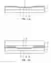
FIGS. 1A-1I are cross sections showing the steps for fabricating an electronic device package 500a such as pressure sensor package according to an embodiment of the invention. As shown in FIG. 1A, a wafer 3 having an upper surface 20 and a lower surface 30 is provided, wherein a plurality of cavities 5 is formed on the lower surface 30 of the wafer 3, wherein the plurality of cavities 5 extend into the wafer 3. The cavities 5 are sealed by a carrier substrate 1 bonded to the lower surface 30 of the wafer 3. The carrier substrate 1 may comprise a glass substrate with a thickness of between about 300 μm and 500 μm, or preferably about 400 μm. In one embodiment, the wafer 3 may be formed of silicon or other materials having good thermal dissipation ability or a high thermal conductivity coefficient. The cavities 5 may be formed by etching the wafer 3 using a process such as a wet etching process. The wafer 3 may have a thickness of between about 100 μm and 200 μm, or preferably about 140 μm. In one embodiment, an adhesive such as epoxy may be used to bond the wafer 3 to the carrier substrate 1. However, the invention is not limited to thereto. In one embodiment, a plurality of micro electro-mechanical devices comprising sensor chips is disposed on the wafer 3. A sensor film 9, for example, a piezoelectrical material film, is formed in the wafer 3 and adjacent to the upper surface 20 of the wafer 3 to measure the changes in the surrounding environment or fluids. The sensor film 9 is surrounded by a conductive electrode or a conductive pad 7. As shown in FIG. 1A, the conductive electrode 7 connects to the sensor film 9 to transfer sensing signals of the sensor film 9. Alternatively, the sensor film 9 may be also formed on the upper surface 20 of the wafer 3, connecting to the conductive electrode 7. Also, the silicon wafer 3 and the conductive electrode 7 are separated by forming an insulating film (not shown), for example, forming a silicon oxide, silicon oxynitride or low dielectric constant material layer, therebetween.
As shown in FIG. 1B, next, a packaging layer or a covering plate 13 may be formed on the upper surface 20 of the wafer 3. In one embodiment, a spacer 11 or a dam may be formed between the covering plate 13 and the conductive electrode 7, thereby forming a cavity 15 between the covering plate 13 and the sensor film 9. The spacer 11 surrounds the cavity 15. The covering plate 13 may comprise, for example, glass, quartz, opal or plastic. In this embodiment, the covering plate 13 is a silicon substrate. The covering plate 13 has an opening formed therein, for fluid to flow in and out of. The covering plate 13 may have a thickness of between about 500 μm and 800 μm, or preferably about 700 μm. The spacer 11 may comprise adhesive materials, for example, epoxy. Generally, the spacer 11 is on the conductive electrode 7.
Next, a step of thinning down the carrier substrate 1 may be optionally performed. For example, a backside 10 of the glass substrate 1 is thinned down to a preferred thickness, for example, from 400 μm to 120 μm, by an etching, milling, grinding or polishing process.
Next, referring to FIG. 1C, an opening 17 is formed at a position below a preferred scribe line or the conductive electrode 7, through the carrier substrate 1 and deep into a portion of the wafer 3. In one embodiment, a notching process may be performed by notch equipment. For example, a knife with a 60 degree cutting angle may cut the carrier substrate 1 and the wafer 3, to form the channel notch 17.
Next, as shown in FIG. 1D, the wafer 3 is etched along the opening 17 to form an opening 19 with a wide lower portion and a narrow upper portion. For example, a silicon etching process is performed on the silicon wafer 3 to remove the wafer material on the sidewalls and a bottom of the opening, wherein the insulating layer between the conductive electrode 7 and the wafer 3 may serve as an etching stop layer in this step.
Referring to FIG. 1E, an opening 21 with a wide upper portion (a portion in the carrier substrate 1) and a narrow lower portion (a portion in the wafer 3) is formed at a position of the opening 19. A notching process may be performed by notch equipment to cut the carrier substrate 1, wherein the knife used in the notching process has a wide width or a large cutting angle. For example, a knife with a cutting angle larger than about 60 degrees is selected. Preferably, a knife with the cutting angle between about 75 and 80 degrees is selected. Therefore, the opening 21 has a wide upper portion (a portion in the carrier substrate 1) and a tilted angle of the wide upper portion is larger than the lower portion (a portion in the wafer 3), thereby facilitating deposition of a conductive line. Additionally, sidewalls of the upper portion (a portion in the carrier substrate 1) and the lower portion (a portion in the wafer 3) of the opening 21 are connected together, thereby preventing voids from being generated while filling in the insulating layer 23 as shown in FIG. 1F.
Referring to FIG. 1F, the insulating layer 23 is formed in the opening 21. In one embodiment, the insulating layer 23 is formed on the backside 10 of the carrier substrate 1, filling the opening 21. Preferably, the insulating layer 23 may be made of epoxy, solder mask or other suitable insulating materials, such as insulating deposited layers including non-organic materials comprising silicon nitride, silicon oxinitride, metal oxide or combinations thereof, or organic materials comprising polyimide, BCB™, parylene, polynaphthalenes, fluorocarbons or accrylates. The insulation layer is preferably formed by a coating method such as spin coating, spray coating or curtain coating, or may be formed by any suitable method, such as a liquid phase deposition, physical vapor deposition, chemical vapor deposition, low pressure chemical vapor deposition, plasma enhanced chemical vapor deposition, rapid thermal chemical vapor deposition or atmospheric pressure chemical vapor deposition process.
Next, referring to FIG. 1G, an opening 25, extending deep into the spacer 11, exposing the conductive electrodes 7, is formed. The insulating layer 23 and the insulating layer between the conductive electrodes 7 and the wafer 3 and a portion of the spacer 11 are patterned to form the opening 25 (not shown) by methods such as a photolithography/etching process. Alternatively, a notching process is performed by notch equipment to cut the insulating layer 23 and the conductive electrodes 7 to a portion of the spacer 11, thereby forming the opening 25 with exposed sides of the conductive electrode 7.
Next, a conductive layer 27 is formed on an inner sidewall and a lower portion of the opening 25, extended over a portion of the insulating layer 23 over the backside 10 of the carrier substrate 1, wherein the conductive layer 27 may electrically connect to the conductive electrode 7. In this embodiment, the conductive layer 27 electrically connects to sides of the conductive electrode 7. Alternatively, the conductive layer 27 may electrically connect to a lower surface of the conductive electrode 7. Generally, the conductive layer 27 may be a conductive material layer formed of Cu, Al, Ag, Ni or alloys thereof. The conductive material layer may be conformably formed on the backside 10 of the carrier substrate 1, extending to a tiled side and the lower portion of the opening 25 by using, for example, an electroplating or sputtering process. Next, a photolithography/etching process is performed to pattern the conductive material layer, thereby forming the conductive layer 27.
Next, as shown in FIG. 1H, a passivation layer 29 is formed on the conductive layer 27, covering the backside 10 of the carrier substrate 1 and filling the opening 25 after forming the conductive layer 27. The passivation layer 29 may be, for example, a solder mask. In one embodiment, the passivation layer 29 may be patterned to form openings 31 exposing a portion of the conductive layer 27 after the passivation layer 29 is formed.
Next, referring to FIG. 1I, before forming conductive bumps 33, an opening 35 communicating with the cavity 15 is formed in the covering plate 13 and over a position corresponding to the sensing film 9, wherein the opening 35 may comprise a single opening or a porous structure to communicate with an outside fluid. Next, the covering plate 13 is thinned down. In one embodiment, an area of the sensing film 9 to an area of the opening 35 is equal to a ratio preferably of between about 1 and 1.5, thereby stabilizing and protecting the covering plate 13 while not affecting the sensing film 9 when the sensing film 9 senses fluid flowing through the opening 35. If the covering plate 13 is formed of silicon, the opening 35 can be formed by a dry etching process. Additionally, the spacer 11 and the sensing film 9 may further comprise a pressure release region 40 therebetween to prevent stress from transmitting from the covering plate 13 to the spacer 11, which may affect detection of the sensing film 9. For example, the spacer 11 and the sensing film may be horizontally separated by a default distance 40 larger than about 100 μm. Alternatively, one or more cavities may be formed on the silicon wafer horizontally between the spacer 11 and the sensing film 9 to prevent stress. Also, the cavities may be filled with buffer materials. Finally, conductive bumps 33 are formed on positions of the openings 31 to electrically connect to the conductive layer 27. In one embodiment, a solder is filled in the opening by an electroplating or screen printing process. A solder re-flow process is performed to form the conductive bumps 33 such as solder balls or solder pastes. Next, the wafer 3 is cut along scribe lines SC to be divided into several individual pressure sensing chips, to complete the formation of the electronic device package 500a.
In the aforementioned embodiments, the opening 35 of the covering plate 13 is exposed after the formation of the passivation layer 29, thereby preventing the sensing film 9 from being contaminated during processes performed before exposure of the covering plate 13. Also, the opening 35 is formed before the formation of the conductive bumps 33, thereby preventing the conductive bumps 33 from being damaged due to processes performed up to the formation of the opening 35.
FIGS. 2A-2E are cross sections showing the steps for fabricating an electronic device package 500b such as pressure sensor package according to another embodiment of the invention. As shown in FIG. 2A, a wafer 3 having an upper surface 20 and a lower surface 30 is provided, wherein a plurality of cavities 5 is formed on the lower surface 30 of the wafer 3, extending into the wafer 3. The cavities 5 are sealed by a carrier substrate 1 bonded to the lower surface 30 of the wafer 3. The carrier substrate 1 may comprise a glass substrate with a thickness of between about 300 μm and 500 μm, or preferably about 400 μm. In one embodiment, the wafer 3 may be formed of silicon or other materials having good thermal dissipation ability or a high thermal conductivity coefficient. The cavities 5 may be formed by etching the wafer 3 using methods such as a wet etching process. The wafer 3 may have a thickness of between about 100 μm and 200 μm, or preferably about 140 μm. In one embodiment, an adhesive such as epoxy may be used to bond the wafer 3 to the carrier substrate 1. However, the invention is not limited to thereto. In one embodiment, a plurality of micro electro-mechanical devices comprising sensor chips is disposed on the wafer 3. A sensor film 9, for example, a piezoelectrical material film, covers the upper surface 20 of the wafer 3 to sense changes in the surrounding environment or fluids. The sensor film 9 is surrounded by an electrode or a conductive pad 7 to transfer sensing signals of the sensor film 9. Also, the silicon wafer 3 and the conductive electrode 7 are separated by forming an insulating film (not shown), for example, forming a silicon oxide, silicon oxynitride or low dielectric constant material layer, therebetween.
As shown in FIG. 2B, next, a packaging layer or a covering plate 53 may be formed on the upper surface 20 of the wafer 3. In one embodiment, a spacer 11 may be formed between the covering plate 53 and the conductive electrode 7, thereby forming a cavity 55. The spacer 11 surrounds the cavity 55. The covering plate 53 may comprise, for example, glass, quartz, opal or plastic. In this embodiment, the covering plate 53 is a silicon substrate. The covering plate 53 has an opening formed therein, for fluid to flow in and out of. The covering plate 53 may have a thickness of between about 200 μm and 400 μm, or preferably about 300 μm. The spacer 11 may comprise adhesive materials, for example, epoxy. Generally, the spacer 11 is on the conductive electrode 7. An opening 65 may be pre-formed in the covering plate 53 and sealed by pasting a sealing layer 67, such as an adhesive tape, to the opening 65. Next, the covering plate 53 is attached to the upper surface of the wafer 3 so that the cavity 55 may communicate the opening 65, wherein the opening 65 may be a single opening or a porous structure.
Next, a step of thinning down the carrier substrate 1 may be optionally performed. For example, a backside 10 of the glass substrate 1 is thinned down to a preferred thickness, for example, from 400 μm to 120 μm, by an etching, milling, grinding or polishing process.
Next, referring to FIG. 2C, an opening 17 is formed at a position below the preferred scribe line or conductive electrode 7, through the carrier substrate 1, extending deep into the wafer 3. In one embodiment, a notching process may be performed by notch equipment. For example, a knife with a 60 degree cutting angle may cut the carrier substrate 1 and the wafer 3, to form the channel notch 17. Next, the wafer 3 is etched along the opening 17 to form an opening 19 with a wide lower portion. For example, a silicon etching process is performed on the silicon wafer 3 to remove the wafer material on the sidewalls and a bottom of the opening, wherein the insulating layer between the conductive electrode 7 and the wafer 3 may serve as an etching stop layer in this step.
Referring to FIG. 2D, an opening 21 with a wide upper portion is formed at a position of the opening 19. A notching process may be performed by notch equipment to cut the carrier substrate 1, wherein the knife used in the notching process has a wide width or a large cutting angle. For example, a knife with the cutting angle larger than about 60 degrees is selected. Preferably, a knife with the cutting angle between about 75 and 80 degrees is selected. Therefore, the opening 21 has a wide upper portion (a portion in the carrier substrate 1) and a tilted angle of the upper portion is larger than the lower portion (a portion in the wafer 3), thereby facilitating conductive line deposition. Additionally, sidewalls of the upper portion (a portion in the carrier substrate 1) and the lower portion (a portion in the wafer 3) of the opening 21 are connected together, thereby preventing voids from being generated while filling the insulating layer 23. Next, the insulating layer 23 is formed in the opening 21. In one embodiment, the insulating layer 23 is formed on the lower surface of the carrier substrate 1, filling the opening 21. Preferably, the insulating layer 23 may be epoxy, solder mask or other suitable insulating materials, such as insulating deposited layers including non-organic materials comprising silicon nitride, silicon oxinitride, metal oxide or combinations thereof, or organic materials comprising polyimide, BCB™, parylene, polynaphthalenes, fluorocarbons or accrylates. The insulation layer is preferably formed by a coating method such as spin coating spray coating or curtain coating, or may be formed by any suitable method, such as, a liquid phase deposition, physical vapor deposition, chemical vapor deposition, low pressure chemical vapor deposition, plasma enhanced chemical vapor deposition, rapid thermal chemical vapor deposition or atmospheric pressure chemical vapor deposition process.
Next, still referring to FIG. 2D, an opening 25, exposing the conductive electrode 7 is formed. The insulating layer 23 and the insulating layer between the electrodes and the wafer are patterned to form the opening 25 (not shown) by a method such as a photolithography/etching process. Alternatively, a notching process is performed by notch equipment to cut the insulating layer 23 and the conductive electrodes 7 to a portion of the spacer 11, thereby forming the opening 25, exposing the sides of the conductive electrode 7.
Next, a conductive layer 27 is formed on an inner sidewall and a lower portion of the opening 25, extending over the insulating layer over the lower surface of the carrier substrate 1, wherein the conductive layer 27 may electrically connect to the conductive electrodes 7. In this embodiment, the conductive layer 27 electrically connects to sides of the conductive electrode 7. Alternatively, the conductive layer 27 may electrically connect to a lower surface of the conductive electrode 7. Generally, the conductive layer 27 may be a conductive material layer formed of Cu, Al, Ag, Ni or alloys thereof. The conductive material layer may be conformably formed on the backside of the carrier substrate 1, extending to a tiled side and the lower portion of the opening 25 by using, for example, by an electroplating or sputtering process. Next, a photolithography/etching process is performed to pattern the conductive material layer, thereby forming the conductive layer 27.
Next, as shown in FIG. 2E, a passivation layer 29 is formed on the conductive layer 27, covering the backside 10 of the carrier substrate 1 and filling the opening 25 after the conductive layer 27 is formed. The passivation layer 29 may be, for example, a solder mask. In one embodiment, the passivation layer 29 may be patterned to form openings 31 exposing a portion of the conductive layer 27 after the passivation layer 29 is formed.
Next, conductive bumps 33 are formed on positions of the openings 31 to electrically connect to the conductive layers 27. In one embodiment, a solder is filled into the opening by an electroplating or screen printing process. A solder re-flow process is performed to form the conductive bumps such as solder balls or solder pastes. After forming the conductive bumps, the adhesive tape 67 is removed to expose the opening 65, which is in the covering plate 13 and over a position corresponding to the sensing film 9, communicating with the cavity 55, wherein the opening may comprise a single opening or a porous structure to communicate with outside fluids. In one embodiment, an area of the sensing film 9 to an area of the opening 65 is equal to a ratio preferably of between about 1 and 1.5, thereby stabilizing and protecting the covering plate 53 while not affecting the sensing film 9 when the sensing film 9 senses fluid flows through the opening 65. Additionally, the spacer 11 and the sensing film 9 may further comprise a pressure release region 40 therebetween to prevent stress from transmitting from the covering plate 13 to the spacer 11, affecting the detection of the sensing film 9. For example, the spacer 11 and the sensing film may be horizontally separated by a default distance 40 such as a default distance larger than about 100 μm. Alternatively, one or more cavities may be formed on the silicon wafer horizontally between the spacer 11 and the sensing film 9 to prevent stress. Also, the cavities may be filled with buffer materials. Finally, the sealing layer 67 such as adhesive tape is torn, and the wafer is cut along scribe lines SC to divide the wafer into several individual pressure sensing chips, thus completing formation of the electronic device package 500b.
In the aforementioned embodiments, the opening 65 is firstly formed in the covering plate 53 and sealed by a sealing layer 67 such as an adhesive tape and then the covering plate 53 is attached to the wafer 3, thereby preventing the sensing film 9 from contamination during the fabricating process.
The exemplary embodiments of the electronic device package 500a pr 500b of the invention are fabricated by a wafer level package process. Therefore, the package may have a smaller size. Additionally, in the electronic device package, conductive layers or conductive bumps rather than bond wires are used to electrically connect to the electrodes of the semiconductor chip. Therefore, package size is further reduced.
While the invention has been described by way of example and in terms of the preferred embodiments, it is to be understood that the invention is not limited to the disclosed embodiments. To the contrary, it is intended to cover various modifications and similar arrangements (as would be apparent to those skilled in the art). Therefore, the scope of the appended claims should be accorded the broadest interpretation so as to encompass all such modifications and similar arrangements.
Claims
What is claimed is:1. A method for fabricating an electronic device package, comprising:
providing a wafer having an upper surface with a conductive electrode disposed thereon and a lower surface;
covering the upper surface of the wafer with a covering plate;
covering the lower surface of the wafer with a passivation layer;
forming conductive bumps on the passivation layer, electrically connected to the conductive electrodes; and
forming an opening structure on the covering plate, wherein the step of forming an opening structure is performed before the step of covering the upper surface of the wafer with the covering plate, or after the step of covering the lower surface of the wafer with the passivation layer and before the step of forming the conductive bumps.
2. The method for fabricating an electronic device package as claimed in claim 1, wherein a plurality of micro electro-mechanical devices is disposed on the wafer.
3. The method for fabricating an electronic device package as claimed in claim 2, wherein the micro electro-mechanical devices comprise pressure sensor chips with sensing films covering upper surfaces thereof.
4. The method for fabricating an electronic device package as claimed in claim 3, further comprising a cavity between the sensing film and the covering plate, surrounded by a spacer, wherein the spacer and the sensing film further comprise a pressure release region therebetween.
5. The method for fabricating an electronic device package as claimed in claim 4, wherein the spacer is between the covering plate and the conductive electrode.
6. The method for fabricating an electronic device package as claimed in claim 4, wherein the spacer and the sensing film are separated by a default distance.
7. The method for fabricating an electronic device package as claimed in claim 1, wherein the opening structure comprises a single opening or a porous structure.
8. The method for fabricating an electronic device package as claimed in claim 1, further comprising forming a plurality of cavities on the lower surface of the wafer, and extending into the wafer, wherein the cavities are sealed by a carrier substrate bonded to the lower surface of the wafer.
9. The method for fabricating an electronic device package as claimed in claim 8, further comprising performing a step of thinning down a backside of the carrier substrate to a preferred thickness.
10. The method for fabricating an electronic device package as claimed in claim 9, wherein the step of thinning down comprises an etching, milling, grinding or polishing process.
11. The method for fabricating an electronic device package as claimed in claim 1, further comprising:
removing a portion of the wafer from the lower surface thereof to form a first opening in a position below the conductive electrode;
forming an insulating layer on the lower surface of the wafer, in the first opening;
removing a portion of the insulating layer in the first opening to form a second opening, exposing the conductive electrode; and
forming a conductive layer on an inner sidewall and a lower portion of the second opening, and extended over a portion of the insulating layer over the lower surface of the wafer, wherein the conductive layer electrically connects to the conductive electrode before covering the lower surface of the wafer with the passivation layer.
12. The method for fabricating an electronic device package as claimed in claim 11, wherein the passivation layer is formed on the conductive layer, filling the second opening.
13. The method for fabricating an electronic device package as claimed in claim 4, wherein the opening structure is formed directly over a position corresponding to the sensing film, communicating with the cavity.
14. The method for fabricating an electronic device package as claimed in claim 3, wherein an area of the sensing film to an area of the opening structure is equal to a ratio of between 1 and 1.5.
15. An electronic device package, comprising:
a sensor chip, wherein an upper surface of the sensor chip comprises a sensing film;
a covering plate having an opening structure covering the sensor chip, wherein the covering plate and the sensor chip have a cavity therebetween, and the cavity is over a position corresponding to the sensing film, communicating with the opening structure; and
a spacer between the covering plate and the sensor chip, surrounding the cavity, wherein the spacer and the sensing film have a pressure release region therebetween.
16. The electronic device package as claimed in claim 15, wherein the spacer and the sensing film further comprise a pressure release region therebetween.
17. The electronic device package as claimed in claim 15, further comprising a conductive electrode disposed on the upper surface of the sensor chip, between the spacer and the sensor chip.
18. The electronic device package as claimed in claim 15, wherein the spacer and the sensing film are separated by a default distance.
19. The electronic device package as claimed in claim 15, wherein the covering plate is a silicon substrate.
20. The electronic device package as claimed in claim 16, wherein the opening structure comprises a single opening or a porous structure.
21. The electronic device package as claimed in claim 7, further comprising a plurality of cavities formed on the lower surface of the sensor chip, extending into the wafer, wherein the cavities are sealed by a carrier substrate bonded to the lower surface of the sensor chip.
22. The electronic device package as claimed in claim 16, further comprising:
an opening from the lower surface of the sensor chip, extending into the sensor chip, wherein the conductive electrode is exposed from a bottom of the opening;
an insulating layer formed on the lower surface of the sensor chip and in the first opening;
a conductive layer formed on an inner sidewall and a lower portion of the opening, extending over a portion of the insulating layer over the lower surface of the wafer, wherein the conductive layer electrically connects to the conductive electrode;
a passivation layer covering the lower surface of the sensor chip; and
a conductive bump formed on the passivation layer, electrically connected to the conductive electrode.
23. The electronic device package as claimed in claim 22, wherein the passivation layer is formed on the conductive layer, filling the opening.
24. The electronic device package as claimed in claim 15, wherein an area of the sensing film to an area of the opening structure is equal to a ratio of between 1 and 1.5.
Images & Drawings included:


Sources:
- United States Patent and Trademark Office - verify current appl. status at the USPTO↗
Similar patent applications:
- » 20160056381
Electronic package device for testing a package effect of the device, fabrication method thereof and method for testing electronic package device - » 20210020679
Electronic device package and fabricating method thereof - » 20220375985
Electronic device package and fabricating method thereof - » 20240347575
Electronic device package and fabricating method thereof - » 20250160031
ELECTRONIC DEVICE PACKAGE AND FABRICATING METHOD THEREOF - » 20110193225
Electronic device package and fabrication method thereof - » 20110233782
Electronic device package and fabrication method thereof - » 20090289345
Electronic device package and fabrication method thereof - » 20130161778
Electronics device package and fabrication method thereof - » 20140193950
Electronic device package and fabrication method thereof
Recent applications in this class:
- » 20240253979 2024-08-01
STRESS ISOLATION PROCESS - » 20230126914 2023-04-27
METHODS AND APPARATUS FOR ELECTRONIC DEVICE PACKAGING - » 20220289565 2022-09-15
MEMS device having decreased contact resistance - » 20220185661 2022-06-16
Mems device having a rugged package and fabrication process thereof - » 20220063994 2022-03-03
MEMS device with dummy-area utilization for pressure enhancement - » 20210061652 2021-03-04
Fabrication method for a MEMS device - » 20200399120 2020-12-24
MEMS vibrator and MEMS oscillator - » 20200131032 2020-04-30
MEMS device with dummy-area utilization for pressure enhancement - » 20200115225 2020-04-16
Process for fabricating a device for detecting electromagnetic radiation having an improved encapsulation structure - » 20200115224 2020-04-16
MEMS DEVICE HAVING A RUGGED PACKAGE AND FABRICATION PROCESS THEREOF