PRINTED CIRCUIT BOARD AND METHOD FOR MAKING SAME
US20110240345A1
2011-10-06
12/764,963
2010-04-22
Abstract:
A printed circuit board (PCB) includes a base, copper foils, an insulating layer, and metallic foils. The copper foils are disposed on the base. The insulating layer is coated on the copper foils. The metallic foils are layered on the insulating layer. The copper foils and the metallic foils connect a first electrical element to a second electrical element.
Assignee:
- HON HAI PRECISION INDUSTRY CO., LTD. 12,828 🇹🇼 Tu-Cheng, Taiwan
Interested in similar patents?
Get notified when new applications in this technology area are published.
Classification:
H05K1/181 » CPC main
Printed circuits; Printed circuits structurally associated with non-printed electric components associated with surface mounted components
H05K1/181 » CPC main
Printed circuits; Printed circuits structurally associated with non-printed electric components associated with surface mounted components
B32B37/02 » CPC further
Methods or apparatus for laminating, e.g. by curing or by ultrasonic bonding characterised by a sequence of laminating steps, e.g. by adding new layers at consecutive laminating stations
B32B2311/00 » CPC further
Inorganic materials used for the layers, laminate or apparatus components
B32B2311/00 » CPC further
Metals, their alloys or their compounds
B32B2311/16 » CPC further
Metals, their alloys or their compounds Tin
B32B2457/08 » CPC further
Electrical equipment PCBs, i.e. printed circuit boards
H05K2201/0352 » CPC further
Indexing scheme relating to printed circuits covered by; Conductive materials; Structure of the conductor; Layered conductors or foils Differences between the conductors of different layers of a multilayer
H05K2201/0352 » CPC further
Indexing scheme relating to printed circuits covered by; Conductive materials; Structure of the conductor; Layered conductors or foils Differences between the conductors of different layers of a multilayer
H05K2201/0979 » CPC further
Indexing scheme relating to printed circuits covered by; Shape and layout; Shape and layout details of conductors covering at least two types of conductors provided for in - Redundant conductors or connections, i.e. more than one current path between two points
H05K2201/0979 » CPC further
Indexing scheme relating to printed circuits covered by; Shape and layout; Shape and layout details of conductors covering at least two types of conductors provided for in - Redundant conductors or connections, i.e. more than one current path between two points
Y02P70/50 » CPC further
Climate change mitigation technologies in the production process for final industrial or consumer products Manufacturing or production processes characterised by the final manufactured product
Y02P70/50 » CPC further
Climate change mitigation technologies in the production process for final industrial or consumer products Manufacturing or production processes characterised by the final manufactured product
Y10T156/10 » CPC further
Adhesive bonding and miscellaneous chemical manufacture Methods of surface bonding and/or assembly therefor
H05K1/09 IPC
Printed circuits; Details Use of materials for the conductive, e.g. metallic pattern
H05K1/09 IPC
Printed circuits; Details Use of materials for the conductive, e.g. metallic pattern
B32B37/00 IPC
Methods or apparatus for making layered products; Treatment of the layers or of the layered products
B32B37/00 IPC
Methods or apparatus for laminating, e.g. by curing or by ultrasonic bonding
Description
BACKGROUND
1. Technical Field
The present disclosure relates to a printed circuit board (PCB) and a method for making the same.
2. Description of Related Art
Generally, a central processing unit (CPU) and a power supply managing circuit are disposed on a printed circuit board (PCB) of a computer and connected to each other via a plurality of copper foils. A heat sink is disposed on the CPU for heat dissipation of the CPU. The volume of the heat sink is typically larger than the CPU. Therefore, it is necessary to leave a space between the CPU and the power supply managing circuit to position the heat sink. As a result, the copper foils are undesirably elongated, resulting in a larger resistance of the copper foils and accordingly a larger amount of power loss.
Therefore, it is desirable to provide a PCB, which can overcome the above-discussed shortcomings.
BRIEF DESCRIPTION OF THE DRAWINGS
Many aspects of the embodiments should be better understood with reference to the following drawings. The components in the drawings are not necessarily drawn to scale, the emphasis instead being placed upon clearly illustrating the principles of the present disclosure. Moreover, in the drawings, like reference numerals designate corresponding parts throughout the several views.
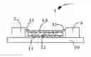
FIG. 1 is a cross-sectional view of a printed circuit board (PCB) according to the disclosure.
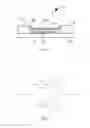
FIG. 2 is a circuit diagram of the PCB of FIG. 1.
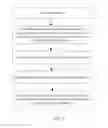
FIG. 3 is a flow chart of a method of making the PCB of FIG. 1.
DETAILED DESCRIPTION
Referring to FIG. 1, a printed circuit board (PCB) 1, according to a disclosure, is configured for connecting a first electrical element to a second electrical element. In the present disclosure, the first electrical element is a CPU 2. The second electrical element is a power supply managing circuit 3. The CPU 2 includes a plurality of input pins 21. The power supply managing circuit 3 is electrically connected to a power supply (not shown) and configured for adjusting the voltage of the power supply to make the CPU 2 to work at a rated voltage and a rated current. The power supply managing circuit 3 includes a plurality of output pins 31. The PCB 1 includes a base 10, a plurality of copper foils 11, an insulating layer 12, and a plurality of metallic foils 13.
The insulating layer 12 is coated on the copper foils 11. The metallic foils 13, such as tin foils, are coated on the insulating layer 12. The copper foils 11 and the metallic foils 13 are used for connecting the output pins 31 of the power supply managing circuit 3 to the corresponding input pins 21 of the CPU 2 in parallel.
Referring to FIG. 2, the resistance of the copper foils 11 is represented as R1. The resistance of the metallic foils 13 is represented as R2. The copper foils 11 are parallelly and electrically connected to the metallic foils 13. As such, the total resistance of the copper foils 11 and the metallic foils 13 is R=R1R2/(R1+R2). It is obvious that R will always be smaller than the R1. The power consumption of the copper foils 11 and the metallic foils 13 is: P=I2R, where P is the power consumption and I is the rated current of the CPU 2. Obviously, power loss is reduced.
Referring to FIG. 3, a method of making the PCB is shown. The method includes the following steps:
S1: providing a PCB 1.
S2: Forming a plurality of copper foils 11 configured for connecting to a number of input pins 21 of a first electrical element 2 and a number of output pins 31 of a second electrical element 3 mounted on the PCB 1. In the present disclosure, the first electrical element is a CPU, while the second electrical element is a power supply managing circuit.
S3: coating an insulating layer 12 on the plurality of copper foils 11. In the present disclosure, the insulating layer 12 is made of scaling powder.
S4: applying a plurality of metallic foils 13 on the insulating layer 12.
S5: connecting the copper foils 11 and the metallic foils 13 to the input pins 21 of the first electrical element 2 and the output pins 31 of the second electrical element 3. In the present disclosure, the metallic foils 13 are made of tin foil.
It will be understood that the above particular embodiments and methods are shown and described by way of illustration only. The principles and the features of the present disclosure may be employed in various and numerous embodiments thereof without departing from the scope of the disclosure as claimed. The above-described embodiments illustrate the scope of the disclosure but do not restrict the scope of the disclosure.
Claims
What is claimed is:1. A printed circuit board (PCB) comprising:
a base;
a plurality of copper foils disposed on the base;
an insulating layer coated on the copper foils;
a plurality of metallic foils coated on the insulating layer;
wherein the copper foils and the metallic foils are electrically connect a first electrical element and a second electrical element.
2. The PCB in claim 1, wherein the metallic foils are made of tin foil.
3. The PCB in claim 2, wherein the insulating layer is made of scaling powder.
4. The PCB in claim 1, wherein the first electrical element is a CPU, and the second electrical element is a power supply managing circuit.
5. A method of making a PCB comprising the following:
providing a PCB;
forming a plurality of copper foils configured for connecting a first electrical element and a second electrical element mounted on the PCB;
coating an insulating layer on the plurality of copper foils;
applying a plurality of metallic foils on the insulating layer; and
connecting the copper foils and the metallic foils to the first electrical element and the second electrical element.
6. The method of making a PCB in claim 5, wherein the metallic foils is made of tin foil.
7. The method of making a PCB in claim 6, wherein the insulating layer is made of scaling powder.
8. The method of making a PCB in claim 5, wherein the first electrical element is a CPU, while the second electrical element is a power supply managing circuit.
Images & Drawings included:
Sources:
- United States Patent and Trademark Office - verify current appl. status at the USPTO↗
Similar patent applications:
- » 20170006701
BIODEGRADABLE PRINTED CIRCUIT BOARDS AND METHODS FOR MAKING THE PRINTED CIRCUIT BOARDS - » 20120219249
Optical printed circuit board, a method of making an optical printed circuit board and an optical waveguide - » 20080044130
Optical printed circuit board, a method of making an optical printed circuit board and an optical waveguide - » 20090294056
Method of making printed wiring board and method of making printed circuit board unit - » 20160023461
Printed circuit board fluid flow structure and method for making a printed circuit board fluid flow structure - » 20090041409
ELECTRO-OPTICAL PRINTED CIRCUIT BOARD AND A METHOD OF MAKING AN ELECTRO-OPTICAL PRINTED CIRCUIT BOARD - » 20070280600
Optical printed circuit board blank, a kit and a method of making an optical printed circuit board - » 20090028496
Electro-optical printed circuit board, a blank and a method of making an electro-optical printed circuit board - » 20090078578
Pre-plating solutions for making printed circuit boards and methods for preparing the same - » 20050157475
Method of making printed circuit board with electroplated conductive through holes and board resulting therefrom
Recent applications in this class:
- » 20250176109 2025-05-29
PRINTED CIRCUIT BOARD - » 20250168986 2025-05-22
CIRCUIT BOARD AND METHOD FOR MANUFACTURING MOUNTING BOARD - » 20250168985 2025-05-22
CIRCUIT BOARD AND METHOD FOR MOUNTING ELECTRONIC COMPONENT - » 20250168984 2025-05-22
PRINTED CIRCUIT BOARD AND SEMICONDUCTOR PACKAGE INCLUDING THE SAME - » 20250159812 2025-05-15
INTEGRATED CIRCUIT STRUCTURE - » 20250159811 2025-05-15
SEMICONDUCTOR STORAGE DEVICE - » 20250159810 2025-05-15
PRINTED CIRCUIT BOARD ASSEMBLY - » 20250151200 2025-05-08
WIRING BOARD, ELECTRONIC COMPONENT MOUNTING PACKAGE USING WIRING BOARD, AND ELECTRONIC MODULE - » 20250151199 2025-05-08
Apparatus and Method for Improving Micro-Inverter Longevity - » 20250142729 2025-05-01
ELECTRONIC DEVICE
Recent applications for this Assignee:
- » 20140233961 2014-08-21
Optical communication module including optical-electrical signal converters and optical signal generators - » 20140083669 2014-03-27
HEAT SINK - » 20140063746 2014-03-06
Electronic device with heat dissipation assembly - » 20140061224 2014-03-06
AUTOMATIC VENDING MACHINE - » 20140060914 2014-03-06
Enclosure with shield apparatus - » 20140058727 2014-02-27
MULTIMEDIA RECORDING SYSTEM AND METHOD - » 20140055955 2014-02-27
Fastener - » 20140055322 2014-02-27
DISPLAY SYSTEM AND HEAD-MOUNTED DISPLAY APPARATUS - » 20140054439 2014-02-27
CONTAINER DATA CENTER WITH SUPPORTING APPARATUS - » 20140054311 2014-02-27
AUTOMATIC VENDING MACHINE WITH MOVING MEMBER FOR PRODUCTS