Silicide contact formation
US20110241213A1
2011-10-06
12/754,912
2010-04-06
✅ Patent granted
US 8,404,589 B2
2013-03-26
-
-
Nitin Parekh
Cantor Colburn LLP | Louis Percello
2030-06-04
Abstract:
A method for forming a silicide contact includes depositing a metal layer on silicon such that the metal layer intermixes with the silicon to form an intermixed region on the silicon; removing an unintermixed portion of the metal layer from the intermixed region; and annealing the intermixed region to form a silicide contact on the silicon. A semiconductor device comprising a silicide contact located over a silicon layer of the semiconductor device, the silicide contact comprising nickel (Ni) and silicon (Si) and having Ni amount equivalent to a thickness of about 21 angstroms or less.
Inventors:
- Yu Zhu 29 🇺🇸 West Harrison, NY, United States
- Stephen Rossnagel 12 🇺🇸 Pleasantville, NY, United States
- Bin Yang 17 🇺🇸 Ossining, NY, United States
- Zhen Zhang 72 🇺🇸 Ossining, NY, United States
- Christian Lavoie 88 🇺🇸 Pleasantville, NY, United States
- Andrew J. Kellock 14 🇺🇸 Sunnyvale, CA, United States
- Stefan Zollner 8 🇺🇸 Hopewell Junction, NY, United States
- Ahmet Ozcan 2 🇺🇸 Pleasantville, NY, United States
Assignee:
- INTERNATIONAL BUSINESS MACHINES CORPORATION 136,239 🇺🇸 ARMONK, NY, United States
- GLOBAL FOUNDRIES INC. 1 🇺🇸 Sunnyvale, CA, United States
- Globalfoundries Inc. 31 Cayman Islands
Applicant:
Interested in similar patents?
Get notified when new applications in this technology area are published.
Classification:
H01L21/44 IPC
Processes or apparatus adapted for the manufacture or treatment of semiconductor or solid state devices or of parts thereof; Manufacture or treatment of semiconductor devices or of parts thereof the devices having at least one potential-jump barrier or surface barrier, e.g. PN junction, depletion layer or carrier concentration layer the devices having semiconductor bodies not provided for in groups, , , and with or without impurities, e.g. doping materials Manufacture of electrodes on semiconductor bodies using processes or apparatus not provided for in groups -
H01L29/785 » CPC further
Semiconductor devices adapted for rectifying, amplifying, oscillating or switching, or capacitors or resistors with at least one potential-jump barrier or surface barrier, e.g. PN junction depletion layer or carrier concentration layer; Details of semiconductor bodies or of electrodes thereof; Multistep manufacturing processes therefor; Types of semiconductor device ; Multistep manufacturing processes therefor controllable by only the electric current supplied, or only the electric potential applied, to an electrode which does not carry the current to be rectified, amplified or switched; Unipolar devices, e.g. field effect transistors; Field effect transistors with field effect produced by an insulated gate having a channel with a horizontal current flow in a vertical sidewall of a semiconductor body, e.g. FinFET, MuGFET
H01L2924/0002 » CPC further
Indexing scheme for arrangements or methods for connecting or disconnecting semiconductor or solid-state bodies as covered by; Technical content checked by a classifier Not covered by any one of groups , and
H01L2924/00 » CPC further
Indexing scheme for arrangements or methods for connecting or disconnecting semiconductor or solid-state bodies as covered by
H01L23/532 IPC
Details of semiconductor or other solid state devices; Arrangements for conducting electric current within the device in operation from one component to another, i.e. interconnections, e.g. wires, lead frames including external interconnections consisting of a multilayer structure of conductive and insulating layers inseparably formed on the semiconductor body characterised by the materials
H01L21/768 IPC
Processes or apparatus adapted for the manufacture or treatment of semiconductor or solid state devices or of parts thereof; Manufacture or treatment of devices consisting of a plurality of solid state components formed in or on a common substrate or of parts thereof; Manufacture of integrated circuit devices or of parts thereof; Manufacture of specific parts of devices defined in group Applying interconnections to be used for carrying current between separate components within a device comprising conductors and dielectrics
Description
FIELD
This disclosure relates generally to the field of formation of silicide contacts for semiconductor devices.
DESCRIPTION OF RELATED ART
A semiconductor device, such as a field effect transistor (FET), may comprise one or more contacts that are used to apply electrical voltage to the semiconductor device in order to power the device. As semiconductor devices become smaller and smaller, the contacts also need to be made commensurately thinner in size. Semiconductor devices comprising 3-dimensional structures may also require conformal formation of ultra-thin silicide contacts.
SUMMARY
In one aspect, a method for forming a silicide contact includes depositing a metal layer on silicon such that the metal layer intermixes with the silicon to form an intermixed region on the silicon; removing an unintermixed portion of the metal layer from the intermixed region; and annealing the intermixed region to form a silicide contact on the silicon.
In one aspect, a semiconductor device comprising a silicide contact located over a silicon layer of the semiconductor device, the silicide contact comprising nickel (Ni) and silicon (Si) and having Ni amount equivalent to a thickness of about 21 angstroms or less.
Additional features are realized through the techniques of the present exemplary embodiment. Other embodiments are described in detail herein and are considered a part of what is claimed. For a better understanding of the features of the exemplary embodiment, refer to the description and to the drawings.
BRIEF DESCRIPTION OF THE SEVERAL VIEWS OF THE DRAWINGS
Referring now to the drawings wherein like elements are numbered alike in the several FIGURES:
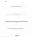
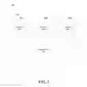
FIG. 1 illustrates an embodiment of a method for formation of a silicide contact.
FIG. 2 illustrates an embodiment of a metal layer deposited on silicon.
FIG. 3 illustrates an embodiment of the device of FIG. 2 after formation of a intermixed layer between the metal layer and the silicon.
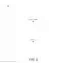
FIG. 4 illustrates an embodiment of the device of FIG. 3 after removal of the unintermixed metal layer from the intermixed layer.
FIG. 5 illustrates an embodiment of a silicide contact after annealing.
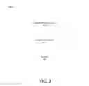
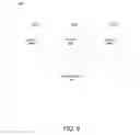
FIG. 6 illustrates an embodiment of a metal layer deposited on 3-D structured silicon on buried oxide.
FIG. 7 illustrates an embodiment of the device of FIG. 6 after formation of a intermixed layer between the metal layer and the silicon.
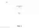
FIG. 8 illustrates an embodiment of the device of FIG. 7 after removal of the unintermixed metal layer from the intermixed layer.
FIG. 9 illustrates an embodiment of conformal silicide contacts after annealing.
DETAILED DESCRIPTION
Embodiments of silicide contacts and methods of forming silicide contacts are provided, with exemplary embodiments being discussed below in detail. A contact for a semiconductor device may comprise a layer of silicide. Semiconductor device scaling requires silicide contact scaling, which calls for formation of extremely thin silicide films for use as contacts. A silicide contact may be formed by sputtering of metal on silicon, annealing to cause the metal and silicon to react, and then removing any unreacted metal. However, it is very difficult to form a conformal silicide due to the poor conformality of the sputtered metal film, especially when the metal thickness is extremely thin. A thin silicide contact having appropriate sheet resistance, composition, phase formation, morphology and thermal stability may be formed by deposition of an appropriate metal on silicon to form an intermixed region between the metal and the silicon, removing any unintermixed metal from the intermixed region, and annealing the intermixed region to form the low resistive phase silicide contact. Formation of the intermixed region is a self-limiting process, and results in a silicide contact having a good conformality and uniformity.
FIG. 1 illustrates an embodiment of a method of forming a thin silicide contact. FIG. 1 is discussed with reference to FIGS. 2-5. In block 101, a metal layer 202 is deposited on silicon 201, as is shown in FIG. 2. Silicon 201 may comprise any silicon portion of any type semiconductor device that requires a contact in operation, and may comprise silicon-on-insulator (SOI) in some embodiments. Metal layer 202 may comprise nickel (Ni) or nickel platinum (NiPt) in some embodiments; if metal layer 202 comprises NiPt, the NiPt may comprise about 10% Pt in some embodiments. In block 102, metal layer 202 and silicon 201 intermix to form intermixed region 301 and unintermixed metal layer 302 on silicon 201, as shown in FIG. 3. The intermixed region 301 forms automatically just after the metal deposition; intermixing of metal layer 202 and silicon 201 is a self-limiting process. In block 103, the unintermixed metal layer 302 is stripped, leaving intermixed region 301 on silicon 201, as shown in FIG. 4. In block 104, the intermixed region 301 and silicon 201 of FIG. 4 are annealed, resulting in silicide contact 501 on silicon 201, as shown in FIG. 5. Silicide contact 501 comprises NiSi or NiPtSi in some embodiments. Silicide contact 501 may be used as an electrical contact for any appropriate semiconductor device, such as a MOSFET. A semiconductor device may comprise any appropriate number of silicide contacts.
FIGS. 6-9 illustrate another embodiment of application of the method 100 of FIG. 1 for conformal formation of silicide contacts on a 3-dimensional silicon structure. In block 101, a metal layer 603 is deposited on 3-dimensional silicon 602A-C, which is located on buried oxide 601, as is shown in FIG. 6. Metal layer 603 may comprise nickel (Ni) or nickel platinum (NiPt) in some embodiments; if metal layer 603 comprises NiPt, the NiPt may comprise between about 10% Pt in some embodiments. In block 102, metal layer 603 and silicon 602A-C intermix to form intermixed regions 701A-C and unintermixed metal layer 702 on silicon 602A-C and buried oxide 601, as shown in FIG. 7. The intermixed regions 701A-C forms automatically just after the metal deposition; intermixing of metal layer 603 and silicon 602A-C is a self-limiting process. In block 103, the unintermixed metal layer 702 is stripped, leaving intermixed regions 701A-C on silicon 602A-C, as shown in FIG. 8. In block 104, the intermixed regions 701A-C are annealed, resulting in conformal silicide contacts 901A-C on 3-dimensional silicon structure 602A-C, as shown in FIG. 9. Silicide contacts 701A-C comprise NiSi or NiPtSi in some embodiments. Silicide contacts 701A-C may be used as an electrical contact for any appropriate semiconductor device, such as a MOSFET. A semiconductor device may comprise any appropriate number of silicide contacts.
The thickness of silicon 201 may have relatively little effect on the qualities (such as thickness and resistance) of silicide contact 501; however, the composition and thickness of metal layer 202 may cause wide variation in the thickness and resistance of silicide contact 501. Use of Ni for metal layer 202 may result in a silicide contact 501 that is epitaxial and has relatively good thermal stability, and also has a relatively uniform thickness. Use of Ni5% Pt for metal layer 202 may result in a silicide contact 501 that is not epitaxial, and may have poor uniformity in thickness. Use of Ni10% Pt may result in a non-epitaxial silicide contact 501 that may have better uniformity of thickness than a contact formed using a metal layer of Ni.
Table 1 below lists Ni amounts (in thicknesses) in the intermixed region that may result from depositing various thicknesses and compositions of metal layer onto silicon.
| TABLE 1 | ||
| Deposited Metal layer | Metal target | Ni amount |
| thickness | composition (atm. %) | in the intermix |
| 1 | nanometer (nm) | Ni | about 10 angstroms (A) |
| 1 | nm | Ni5% Pt | about 11 A |
| 1 | nm | Ni10% Pt | about 11 A |
| 2 | nm | Ni | about 16 A |
| 2 | nm | Ni5% Pt | about 20 A |
| 2 | nm | Ni10% Pt | about 21 A |
| 4 | nm | Ni | about 16 A |
| 4 | nm | Ni5% Pt | about 14 A |
| 4 | nm | Ni10% Pt | about 14 A |
| 6 | nm | Ni | about 16 A |
| 6 | nm | Ni5% Pt | about 14 A |
| 6 | nm | Ni10% Pt | about 14 A |
| 8 | nm | Ni | about 15 A |
| 8 | nm | Ni5% Pt | about 14 A |
| 8 | nm | Ni10% Pt | about 15 A |
| 10 | nm | Ni | about 16 A |
| 10 | nm | Ni5% Pt | about 14 A |
| 10 | nm | Ni10% Pt | about 15 A |
| 15 | nm | Ni | about 17 A |
| 15 | nm | Ni5% Pt | about 13 A |
| 15 | nm | Ni10% Pt | about 15 A |
| 20 | nm | Ni | about 17 A |
| 20 | nm | Ni5% Pt | about 13 A |
| 20 | nm | Ni10% Pt | about 15 A |
Table 2 below lists percentages of Pt in the intermixed region that may result from various thicknesses and compositions of the metal layer.
| TABLE 2 | ||
| Deposited | Metal target | |
| Metal layer thickness | composition (atm. %) | Intermixed region % Pt |
| 1 | nm | Ni5% Pt | about 4.5% |
| 1 | nm | Ni10% Pt | about 7% |
| 2 | nm | Ni5% Pt | about 3.8% |
| 2 | nm | Ni10% Pt | about 7% |
| 4 | nm | Ni5% Pt | about 9% |
| 4 | nm | Ni10% Pt | about 16% |
| 6 | nm | Ni5% Pt | about 11% |
| 6 | nm | Ni10% Pt | about 15.5% |
| 8 | nm | Ni5% Pt | about 9.5% |
| 8 | nm | Ni10% Pt | about 16% |
| 10 | nm | Ni5% Pt | about 11% |
| 10 | nm | Ni10% Pt | about 15.5% |
| 15 | nm | Ni5% Pt | about 11% |
| 15 | nm | Ni10% Pt | about 15.5% |
| 20 | nm | Ni5% Pt | about 9% |
| 20 | nm | Ni10% Pt | about 16% |
Table 3 below lists sheet resistances of a silicide contact that may result from various thicknesses and compositions of the metal layer. A relatively low resistance for silicide contact is desirable for efficient operation of the semiconductor device comprising the silicide contact.
| TABLE 3 | ||
| Deposited | Metal target | Resistance of contact |
| Metal layer thickness | composition (atm. %) | (Ω/□) |
| 1 | nm | Ni | about 250 |
| 1 | nm | Ni5% Pt | about 350 |
| 1 | nm | Ni10% Pt | about 510 |
| 2 | nm | Ni | about 150 |
| 2 | nm | Ni5% Pt | about 150 |
| 2 | nm | Ni10% Pt | about 260 |
| 4 | nm | Ni | about 150 |
| 4 | nm | Ni5% Pt | about 225 |
| 4 | nm | Ni10% Pt | about 200 |
| 6 | nm | Ni | about 150 |
| 6 | nm | Ni5% Pt | about 200 |
| 6 | nm | Ni10% Pt | about 200 |
| 8 | nm | Ni | about 150 |
| 8 | nm | Ni5% Pt | about 370 |
| 8 | nm | Ni10% Pt | about 200 |
| 10 | nm | Ni | about 150 |
| 10 | nm | Ni5% Pt | about 200 |
| 10 | nm | Ni10% Pt | about 200 |
| 15 | nm | Ni | about 150 |
| 15 | nm | Ni5% Pt | about 350 |
| 15 | nm | Ni10% Pt | about 200 |
| 20 | nm | Ni | about 150 |
| 20 | nm | Ni5% Pt | about 250 |
| 20 | nm | Ni10% Pt | about 200 |
The technical effects and benefits of exemplary embodiments include conformal formation of a relatively thin silicide contact in a self-limiting way for use in a semiconductor device.
The terminology used herein is for the purpose of describing particular embodiments only and is not intended to be limiting of the invention. As used herein, the singular forms “a”, “an”, and “the” are intended to include the plural forms as well, unless the context clearly indicates otherwise. It will be further understood that the terms “comprises” and/or “comprising,” when used in this specification, specify the presence of stated features, integers, steps, operations, elements, and/or components, but do not preclude the presence or addition of one or more other features, integers, steps, operations, elements, components, and/or groups thereof.
The corresponding structures, materials, acts, and equivalents of all means or step plus function elements in the claims below are intended to include any structure, material, or act for performing the function in combination with other claimed elements as specifically claimed. The description of the present invention has been presented for purposes of illustration and description, but is not intended to be exhaustive or limited to the invention in the form disclosed. Many modifications and variations will be apparent to those of ordinary skill in the art without departing from the scope and spirit of the invention. The embodiment was chosen and described in order to best explain the principles of the invention and the practical application, and to enable others of ordinary skill in the art to understand the invention for various embodiments with various modifications as are suited to the particular use contemplated.
Claims
1. A method for forming a silicide contact, the method comprising:
depositing a metal layer on silicon such that the metal layer intermixes with the silicon to form an intermixed region on the silicon;
removing an unintermixed portion of the metal layer from the intermixed region; and
annealing the intermixed region to form a silicide contact on the silicon.
2. The method of claim 1, wherein the metal layer comprises nickel (Ni).
3. The method of claim 2, wherein the metal layer has a thickness of 4 nanometers or more, and the intermixed region contains Ni equivalent to a thickness about 10 angstroms to about 18 angstroms.
4. The method of claim 3, wherein the silicide contact has a resistance of about 150Ω/□.
5. The method of claim 2, wherein the silicide contact is epitaxial.
6. The method of claim 1, wherein the metal layer comprises nickel platinum (NiPt).
7. The method of claim 6, wherein the metal layer comprises 10% Pt.
8. The method of claim 7, wherein the metal layer has a thickness of about 4 nanometers or more, and the intermixed region contains Ni equivalent to a thickness between about 11 angstroms and about 21 angstroms.
9. The method of claim 8, wherein the silicide contact comprises about 16% Pt.
10. The method of claim 8, wherein the silicide contact has a resistance of about 200Ω/□.
11. The method of claim 6, wherein the silicide contact is non-epitaxial.
12. The method of claim 1, further comprising forming an electrical connection to the silicide contact to power a field effect transistor (FET).
13. The method of claim 1, wherein the silicon comprises a 3-dimensional silicon structure, and wherein the silicide contact comprises a conformal silicide contact.
14. A semiconductor device comprising a silicide contact located over a silicon layer of the semiconductor device, the silicide contact comprising nickel (Ni) and silicon (Si) and having Ni amount equivalent to a thickness of about 21 angstroms or less.
15. The semiconductor device of claim 14, wherein the silicide contact is epitaxial, and has a resistance of about 150Ω/□.
16. The semiconductor device of claim 14, wherein the silicide contact further comprises about 16% platinum (Pt).
17. The semiconductor device of claim 14, wherein the silicide contact is non-epitaxial, and has a resistance of about 200Ω/□.
18. The semiconductor device of claim 14, wherein the silicon layer of the semiconductor device comprises a 3-dimensional silicon structure, and wherein the silicide contact comprises a conformal silicide contact.
Images & Drawings included:


Sources:
- United States Patent and Trademark Office - verify current appl. status at the USPTO↗
Similar patent applications:
- » 20150372099
CONTACT SILICIDE FORMATION USING A SPIKE ANNEALING PROCESS - » 20250246434
METAL SILICIDE CONTACT FORMATION - » 20150064863
Maskless dual silicide contact formation - » 20150380509
Formation of silicide contacts in semiconductor devices - » 14527300
Directional pre-clean in silicide and contact formation - » 20150206881
Formation of silicide contacts in semiconductor devices - » 20160126102
Directional pre-clean in silicide and contact formation - » 20090114997
Reduced metal pipe formation in metal silicide contacts - » 20080138985
Method for improved formation of nickel silicide contacts in semiconductor devices - » 20140361376
Dielectric liner added after contact etch before silicide formation
Recent applications in this class:
- » 20250266260 2025-08-21
SEMICONDUCTOR DEVICE AND METHOD OF MANUFACTURING SEMICONDUCTOR DEVICE - » 20250253155 2025-08-07
SEMICONDUCTOR DEVICE AND METHOD FOR FORMING THE SAME - » 20250246434 2025-07-31
METAL SILICIDE CONTACT FORMATION - » 20250183040 2025-06-05
SEMICONDUCTOR DEVICES AND METHODS OF MANUFACTURING - » 20250183039 2025-06-05
INTEGRATED CIRCUIT WITH SILICIDE FORMATION BLOCKING - » 20250166996 2025-05-22
SEMICONDUCTOR DEVICE AND METHOD FOR MANUFACTURING THE SAME - » 20250087491 2025-03-13
CONTACT RESISTANCE REDUCTION FOR TRANSISTORS - » 20250054767 2025-02-13
SELECTIVE METAL CAPPING PROCESSES FOR A JUNCTION SILICIDE - » 20250038003 2025-01-30
LOW TEMPERATURE MOLYBDENUM DEPOSITION ASSISTED BY SILICON-CONTAINING REACTANTS - » 20240387180 2024-11-21
DEPOSITION WINDOW ENLARGEMENT
Recent applications for this Assignee:
- » 20250294045 2025-09-18
THREAT POLICY FINE-TUNING BASED ON THE VULNERABILITY OF A SUBNET AS A SOURCE OF A MALICIOUS ATTACK - » 20250294041 2025-09-18
DEVICE POPULATION ANOMALY DETECTION - » 20250292574 2025-09-18
SCENE PARSING - » 20250292026 2025-09-18
A GENERATIVE ARTIFICIAL INTELLIGENCE COMMENTARY - » 20250291689 2025-09-18
MACHINE LEARNING MODEL TRAINING TO ASSIST IN SYSTEM DEBUG - » 20250287215 2025-09-11
PORTABLE MEDIA GEOFENCE AND DEVICE PAIRING SECURITY - » 20250285610 2025-09-11
RECIPIENT-SPECIFIC VOICE TONE ADJUSTMENT IN TELEPHONY - » 20250284728 2025-09-11
CONTEXT LARGE LANGUAGE MODEL OUTPUT EXPLANATION - » 20250278669 2025-09-04
COUNTERFACTUALS WITH FEATURE PREFERENCES FOR CONSISTENT AND DIVERSE EXPLANATIONS - » 20250274345 2025-08-28
MULTI-LAYER EDGE ARCHITECTURE SIMULATION