Stacking integrated circuits containing serializer and deserializer blocks using through silicon via
US20110278737A1
2011-11-17
13/192,217
2011-07-27
✅ Patent granted
US 10,236,275 B2
2019-03-19
-
-
Yuriy Semenenko
Aslan Law, P.C.
2031-07-27
Abstract:
Methods and systems for stacking multiple chips with high speed serialiser/deserialiser blocks are presented. These methods make use of Through Silicon Via (TSV) to connect the dice to each other, and to the external pads. The methods enable efficient multilayer stacking that simplifies design and manufacturing, and at the same time, ensure high speed operation of serialiser/deserialiser blocks, using the TSVs.
Assignee:
- BroadPak Corporation 19 🇺🇸 San Jose, CA, United States
Applicant:
Interested in similar patents?
Get notified when new applications in this technology area are published.
Classification:
H01L25/0657 » CPC main
Assemblies consisting of a plurality of individual semiconductor or other solid state devices ; Multistep manufacturing processes thereof all the devices being of a type provided for in the same subgroup of groups - , e.g. assemblies of rectifier diodes the devices not having separate containers the devices being of a type provided for in group Stacked arrangements of devices
H01L2224/45099 » CPC further
Indexing scheme for arrangements for connecting or disconnecting semiconductor or solid-state bodies and methods related thereto as covered by; Means for bonding being attached to, or being formed on, the surface to be connected, e.g. chip-to-package, die-attach, "first-level" interconnects; Manufacturing methods related thereto; Wire connectors; Manufacturing methods related thereto; Structure, shape, material or disposition of the wire connectors prior to the connecting process of an individual wire connector; Core members of the connector Material
H01L2924/207 » CPC further
Indexing scheme for arrangements or methods for connecting or disconnecting semiconductor or solid-state bodies as covered by; Parameters Diameter ranges
H01L2924/181 » CPC further
Indexing scheme for arrangements or methods for connecting or disconnecting semiconductor or solid-state bodies as covered by; Details of package parts other than the semiconductor or other solid state devices to be connected Encapsulation
H01L2924/00012 » CPC further
Indexing scheme for arrangements or methods for connecting or disconnecting semiconductor or solid-state bodies as covered by; Technical content checked by a classifier Relevant to the scope of the group, the symbol of which is combined with the symbol of this group
H01L2224/73265 » CPC further
Indexing scheme for arrangements for connecting or disconnecting semiconductor or solid-state bodies and methods related thereto as covered by; Means for bonding being of different types provided for in two or more of groups; Location after the connecting process on different surfaces Layer and wire connectors
H01L2924/00 » CPC further
Indexing scheme for arrangements or methods for connecting or disconnecting semiconductor or solid-state bodies as covered by
H01L24/48 » CPC further
Arrangements for connecting or disconnecting semiconductor or solid-state bodies; Methods or apparatus related thereto; Means for bonding being attached to, or being formed on, the surface to be connected, e.g. chip-to-package, die-attach, "first-level" interconnects; Manufacturing methods related thereto; Wire connectors; Manufacturing methods related thereto; Structure, shape, material or disposition of the wire connectors after the connecting process of an individual wire connector
H01L23/481 » CPC further
Details of semiconductor or other solid state devices; Arrangements for conducting electric current to or from the solid state body in operation, e.g. leads, terminal arrangements ; Selection of materials therefor Internal lead connections, e.g. via connections, feedthrough structures
H01L23/00 IPC
Details of semiconductor or other solid state devices
H01L2225/06513 » CPC further
Details relating to assemblies covered by the group but not provided for in its subgroups; All the devices being of a type provided for in the same subgroup of groups - the devices not having separate containers the devices being of a type provided for in group; Stacked arrangements of devices Bump or bump-like direct electrical connections between devices, e.g. flip-chip connection, solder bumps
H01L2225/06517 » CPC further
Details relating to assemblies covered by the group but not provided for in its subgroups; All the devices being of a type provided for in the same subgroup of groups - the devices not having separate containers the devices being of a type provided for in group; Stacked arrangements of devices Bump or bump-like direct electrical connections from device to substrate
H01L2225/06527 » CPC further
Details relating to assemblies covered by the group but not provided for in its subgroups; All the devices being of a type provided for in the same subgroup of groups - the devices not having separate containers the devices being of a type provided for in group; Stacked arrangements of devices Special adaptation of electrical connections, e.g. rewiring, engineering changes, pressure contacts, layout
H01L2225/06541 » CPC further
Details relating to assemblies covered by the group but not provided for in its subgroups; All the devices being of a type provided for in the same subgroup of groups - the devices not having separate containers the devices being of a type provided for in group; Stacked arrangements of devices Conductive via connections through the device, e.g. vertical interconnects, through silicon via [TSV]
H01L2924/00014 » CPC further
Indexing scheme for arrangements or methods for connecting or disconnecting semiconductor or solid-state bodies as covered by; Technical content checked by a classifier the subject-matter covered by the group, the symbol of which is combined with the symbol of this group, being disclosed without further technical details
H01L2924/10253 » CPC further
Indexing scheme for arrangements or methods for connecting or disconnecting semiconductor or solid-state bodies as covered by; Details of semiconductor or other solid state devices to be connected; Material of the semiconductor or solid state bodies; Semiconducting materials; Elemental semiconductors, i.e. Group IV Silicon [Si]
H01L2924/14 » CPC further
Indexing scheme for arrangements or methods for connecting or disconnecting semiconductor or solid-state bodies as covered by; Details of semiconductor or other solid state devices to be connected; Device type Integrated circuits
H01L2924/19041 » CPC further
Indexing scheme for arrangements or methods for connecting or disconnecting semiconductor or solid-state bodies as covered by; Details of hybrid assemblies other than the semiconductor or other solid state devices to be connected; Structure; Component type being a capacitor
H01L2924/30107 » CPC further
Indexing scheme for arrangements or methods for connecting or disconnecting semiconductor or solid-state bodies as covered by; Technical effects; Electrical effects Inductance
Y10T29/53174 » CPC further
Metal working; Means to assemble or disassemble; Means to assemble electrical device Means to fasten electrical component to wiring board, base, or substrate
Y10T29/53178 » CPC further
Metal working; Means to assemble or disassemble; Means to assemble electrical device; Means to fasten electrical component to wiring board, base, or substrate Chip component
Y10T29/53183 » CPC further
Metal working; Means to assemble or disassemble; Means to assemble electrical device; Means to fasten electrical component to wiring board, base, or substrate Multilead component
H05K1/11 IPC
Printed circuits; Details Printed elements for providing electric connections to or between printed circuits
H05K1/11 IPC
Printed circuits; Details Printed elements for providing electric connections to or between printed circuits
H01L25/065 IPC
Assemblies consisting of a plurality of individual semiconductor or other solid state devices ; Multistep manufacturing processes thereof all the devices being of a type provided for in the same subgroup of groups - , e.g. assemblies of rectifier diodes the devices not having separate containers the devices being of a type provided for in group
H01L23/48 IPC
Details of semiconductor or other solid state devices Arrangements for conducting electric current to or from the solid state body in operation, e.g. leads, terminal arrangements ; Selection of materials therefor
H01L23/66 » CPC further
Details of semiconductor or other solid state devices; Structural electrical arrangements for semiconductor devices not otherwise provided for, e.g. in combination with batteries; Impedance arrangements High-frequency adaptations
H01L2225/06572 » CPC further
Details relating to assemblies covered by the group but not provided for in its subgroups; All the devices being of a type provided for in the same subgroup of groups - the devices not having separate containers the devices being of a type provided for in group; Stacked arrangements of devices Auxiliary carrier between devices, the carrier having an electrical connection structure
Description
RELATED APPLICATIONS
This application is a continuation of another U.S. patent application Ser. No. 12/205,875, filed Sep. 6, 2008, with the same assignee, title, and inventor, which is now allowed, and soon to become a US patent. All of the teachings of the U.S. patent application Ser. No. 12/205,875 are incorporated herein, in the current application, by reference.
BACKGROUND OF THE INVENTION
A Serializer/Deserializer (SER/DES) is a pair of functional blocks [integrated circuits or IC/chip] commonly used in high speed communications. These blocks convert data between serial data and parallel interfaces in each direction. Although the term “SER/DES” is generic, in speech it is sometimes used as a more pronounceable synonym for Serial Gigabit Media Independent Interface (SGMII).
SER/DES chips facilitate the transmission of parallel data between two points over serial streams, reducing the number of data paths and thus, the number of connecting pins or wires required. Most SER/DES devices are capable of full duplex operation, meaning that data conversion can take place in both directions simultaneously. SER/DES chips are used in many application including Gigabit Ethernet systems, wireless network routers, fiber optic communications systems, storage applications just to name a few.
Specifications and speeds vary depending on the needs of the user and on the application. These blocks are often integrated within another Integrated Circuit (i.e. ASIC).
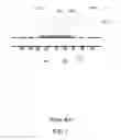
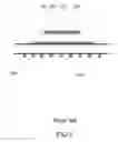
The quest for “smaller, chipper, faster” devices is ever increasing. IC packaging is one area that this quest is continuously challenged. In IC packaging chips are mounted on and connected to a rigid laminate (substrate) via wirebonds (FIG. 1) or bumps in flip chip (FIG. 2) applications. In wirebond technology (FIG. 1) the silicon die (102) is connected via wires (108) to solder mask (106) over a rigid laminate (103). The solder mask (106) is then connected to solder balls (104) through Via holes (107) inside the rigid laminate (103). In flip chip technology (FIG. 2), the silicon die (201) is connected to a substrate (203) via balls (202) and the substrate (203) routes the metal to proper solder balls (204).
Packaging SER/DES is a very challenging and specialized area in the world of IC packaging. With higher data rate flip chips are adapted for packaging high speed SER/DES because in Flip Chip packaging wirebonds are replaced by conductive solder bumps thereby wirebond inductance is no longer present.
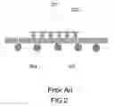
At the present, industry is moving toward 3D packaging where two or more dice are stacked on the top of each other or packages are stacked on the top of packages. These packaging methods offer high density integration in smaller footprint making it suitable for applications in which size matters such as cell phone. FIG. 3 is an example of two equal size chips placed vertically in the same package, in which the chips are connected to the solder balls (305) using wirebond technology. As can be seen from FIG. 3, a first die (301) is placed above a second dies (302), which in turn is placed above a substrate (306). A spacer (303) is placed between the two dies. Another spacer (304) is placed between the bottom die (302) and the substrate (306). FIG. 4 is another example of 3D chip stacking in which the SER/DES die (404) is not stacked and is positioned as a side die beside the stacked dice (401 and 403).
The drawback of stacked die packaging is the use of wirebond, making it unsuitable for high speed SER/DES packaging. In order to circumvent this impediment, this invention proposes to use Through Silicon Via (TSV) to connect dice vertically.
The benefits of using TSV to connect dice vertically are:
1. Higher degree of miniaturization: By placing TSV within the SER/DES block one can facilitate the connection of the die above or below that would otherwise be placed side by side. In a case where non SER/DES dice are stacked with wirebond and SER/DES die is placed next to it, using TSV will eliminate all wires.
2. Placing TSV makes it possible to stack two or more dice with SER/DES block
3. Electrical superiority: When using TSV, it is possible to stack and connect very high data rate SER/DES blocks vertically without the need for any wire.
4. Better thermal performance: The TSV placed within the SER/DES block provides a highly conductive passage for heat removal from the die above.
5. No need for spacer material: Normally, thick Spacer materials are placed between the dice to make wire-bonding of same or different die size possible. Using TSV eliminates the need for this material thereby reducing the cost as well as decreasing the overall height of the package making it possible to fit the package in places where height is a constraint such as very thin cell phones.
This patent claims the placement of TSV within the SER/DES block to enable high density packaging of dice with SER/DES blocks or any other block.
SUMMARY OF THE INVENTION
This invention uses techniques to enable connecting multiple chips (dice) vertically to create a compact 3D chip package. Specifically, it uses techniques that enable high speed SER/DES circuits get connected between multiple dice or from a die to external pins via Through Silicon Via (TSV) that will reduce or eliminate the inductance and capacitance associated with otherwise using wirebond. The techniques for stacking multiple high speed chips enables efficient routing of TSV between different dice that simplifies 3D chip design and manufacturing by providing guidelines on positioning and aligning the chips and by providing guidelines for creating redistribution layer (RDL) and routes that are resistant to stress.
BRIEF DESCRIPTION OF THE DRAWINGS
FIG. 1 shows an example of chip with wirebonded package.
FIG. 2 shows an example of chip with Flip Chip package.
FIG. 3 shows an example of stacked die packing of two chips of the same size using wirebond.
FIG. 4 shows an example of stacked die packing of two chips with a separate SER/DES die in the same package using wirebond.
FIG. 5 shows an example of Trough Silicon Via (TSV) on the SER/DES blocks of a chip placed at the peripheries of the chip.
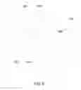
FIG. 6 shows three stacked chips connected to substrate via TSVs.
FIG. 7 shows redistribution layer (Interposer) that is used to route and connected TSVs and Pads.
FIG. 8 shows two chips with TSVs connected to each other through a redistribution layer (Interposer).
FIG. 9 shows TSVs of one chip connected to the pads of another chip through a redistribution layer (Interposer).
FIG. 10 shows the location of test pads at the very edge of dice, when they are stacked on each other.
DETAILED DESCRIPTION OF THE PREFERRED EMBODIMENTS
To create a more compact and space efficient integrated circuit, it is necessary to be able to stack multiple dice on top of each other. Two general methods are possible for interconnecting the stacked dice to each other and for connecting those dice to the pins or solder balls of the 3D chip package. One method is to use wirebond, meaning that to use wires to connect chips to each other or to the pins of the 3D package as shown in FIG. 3 and FIG. 4. The wirebond technique is not very useful for high speed SER/DES due to creation of inductance and capacitance.
Another technique is to use Through Silicon Via (TSV) to connect multiple stacked dice to each other or to the external pins. FIG. 8 shows an example of TSVs (801, 803) of two dice (802, 804) connected to each other. While FIG. 9 shows the contact pads (901) of one die (902) is connected to the TSVs (903) of another die (904). TSVs has so far been only used for lower speed integrated circuits. This patent extends the TSV technology for usage with high speed SER/DES circuits. Doing so would eliminate the need for wirebond and would create a more compact package with superior electrical and thermal characteristics.
And, finally, to test dice which are stacked on each other, test pads need to be created for each die. The test pads must be located at the extreme periphery or edge of dice. FIG. 10 shows two dice (1001, 1003) are stacked on top of each other, They both have TSVs (1005) and the test pads (1002, 1004) are placed at the edge of these dice.
In order to successfully use TSV for the SER/DES circuits a number of rules have to be followed. This patent provides the techniques for using TSV in high speed SER/DES block of chips that could be used for connecting the SER/DES circuit to external pins.
The first technique is to have the SER/DES blocks that use TSV at one or more peripheries of the die. FIG. 5 is an example of such method in which four SER/DES blocks (501) are used at the four peripheries of the die (503) and the SER/DES blocks are equipped with TSVs (502) that can be used to pass through lower dice and get connected to external pins or other dice.
The second technique is to try to limit the SER/DES blocks that use TSV to one or more peripheries of the die and rotate the upper and lower stacked dice by 90 degrees or have the SER/DES staggered so that the SER/DES blocks of those dice will not block each other. This method makes the TSV creation and routing in the interposer layer much easier.
The third technique is to use a redistribution layer (RDL) or interposer when TSVs of the lower and upper die can't be aligned to each other. Redistribution layer (RDL) is used to route and connect TSV to “contact pad”. The trace routes can be of any shape, angle or material. There could be solder resist on the top of RDL and adhesive such as (BCB), etc. FIG. 6 shows an example in which the TSVs of 3 stacked dice are aligned to each other and therefore no RDL is required. While FIG. 7 shows an example, in which the TSVs of the two dice (706, 708) are not aligned to each other and therefore an RDL (707) is required between two dice (706, 708) to route the TSVs. The RDL may contain TSV, blind via, buried via, or any combination of via. The RDL may or may not contain plans, or passive elements such as capacitors. FIG. 8 shows another example of a RDL (805) that is used to connect the via (801) of the top die (802) to the via (803) of the bottom die (804).
The fourth technique is the method for aligning stacked dice. Dice can be aligned using fiducials of any type, such as cross, square, circle, +, −, =, etc, or any text character. Fiducials can be used on the interposer and/or dice for the purpose of alignment. The interposer and dice can have one, two or as many Fiducials, as needed.
The fifth technique is to create (deposit) contact pads on RDL to create a contact point for the other dice TSV. This pad can of any material, size or shape. A circular contact pad (704) is shown in FIG. 7 that resides in the RDL (707). The contact pad (704) is used to connect the TSV of the upper layer (708) to the trace (705) on the RDL and subsequently to the TSV of the lower die (702).
The sixth technique is use tear drops for connecting traces on the RDL to TSVs for the purposes of reinforcement and stress reduction. FIG. 7 shows an example of a tear drop (709) on the TSV of the lower die (702).
The seventh technique is mix wirebond and TSV in stacked chips. Wirebond could be used for low speed digital circuits, while TSV could be used for the high speed SER/DES circuits.
The eight technique is to place the test pads for testing a die that uses TSV at the extreme periphery of the die.
Any variations of the above are also intended to be covered by the application here.
Claims
1. A system for stacking Integrated Circuits vertically to create a three dimensional chip package, said system comprising:
dies;
one or more redistribution layers;
one or more through dies vias through dies vias;
one or more contact pads;
first circuits;
wherein said dies comprise said first circuits;
wherein said first circuits are located on said dies;
wherein said dies are stacked vertically on top of each other in such a way that
wherein one or more fiducials are placed to optically align said dies that are stacked vertically on top of each other;
wherein said one or more through dies vias are placed in said first circuits;
wherein at least one of said one or more redistribution layers is placed between two of said dies;
wherein said dies along with said one or more redistribution layers are stacked on top of a substrate;
wherein said one or more contact pads are placed on said substrate;
wherein said one or more redistribution layers are positioned to interconnect said one or more through dies vias belonging to said two of said dies or to interconnect said one or more through dies vias to said one or more contact pads.
2. A system as stated in claim 1, wherein said one or more fiducials are one of cross, square, circle, or equal symbols.
3. A system as stated in claim 1, wherein said first circuits are placed at one or more areas of said dies, and wherein said dies are stacked vertically on top of each other by rotating said dies in multiples of ninety degrees in such a way that said first circuits placed at said one or more areas of said stacked dies do not block each other.
4. A system as stated in claim 1, wherein said dies and said one or more redistribution layers comprise said one or more through dies vias, blind vias, buried vias, or any combination of vias.
5. A system as stated in claim 1, wherein said one or more contact pads are positioned on said one or more redistribution layers to create contact point for said one or more through dies vias.
6. A system as stated in claim 1, wherein teardrop connections are placed for connecting traces on said one or more redistribution layers to said one or more through dies vias.
7. A system as stated in claim 1, wherein said dies comprise digital circuits or radio frequency circuits.
8. A system as stated in claim 1, wherein said dies connect through said one or more through dies vias for said first circuits, and through wirebonds or flip chips or both wirebonds and flip chips for digital circuits.
9. A system as stated in claim 1, wherein said chip package comprises flip-chip technology, wirebond technology, or combination of both flip-chip technology and wirebond technology.
10. A system as stated in claim 1, wherein one or more of said first circuits are Serial Gigabit Media Independent Interface type.
11. A system as stated in claim 1, wherein said first circuits operate in a full-duplex mode.
12. A system as stated in claim 1, wherein said first circuits operate at radio frequencies.
13. A system as stated in claim 1, wherein said one or more through dies vias are scattered in middle of said dies, and one or more test pads are placed at the extreme periphery of said dies.
14. A system as stated in claim 1, wherein said one or more redistribution layers contain circuit components, interconnects, surface mounts, or embedded passives.
15. A system as stated in claim 1, wherein said three dimensional chip is placed in a Gigabit Ethernet system, a system to serialize or deserialize data, FPGA, or graphics, multimedia, or security chipsets.
16. A system as stated in claim 1, wherein said three dimensional chip is placed in a wireless network router.
17. A system as stated in claim 1, wherein said three dimensional chip is placed in a fiber optic communication or storage system.
18. A system as stated in claim 1, wherein said three dimensional chip is placed in a cellular phone.
19. A system as stated in claim 1, wherein said one or more contact pads are circular.
20. A system as stated in claim 1, wherein said one or more redistribution layers are covered with a solder resist or adhesive.
Images & Drawings included:


Sources:
- United States Patent and Trademark Office - verify current appl. status at the USPTO↗
Similar patent applications:
Recent applications in this class:
- » 20250293212 2025-09-18
SEMICONDUCTOR PACKAGES - » 20250293211 2025-09-18
HEAT DISSIPATION FOR STACKED INTEGRATED CIRCUIT DEVICES - » 20250293210 2025-09-18
SYSTEMS AND METHODS FOR PACKAGING A SEMICONDUCTOR DEVICE - » 20250286021 2025-09-11
SEMICONDUCTOR PACKAGE - » 20250286020 2025-09-11
SEMICONDUCTOR BONDING STRUCTURE - » 20250286019 2025-09-11
SEMICONDUCTOR PACKAGE - » 20250286018 2025-09-11
METHOD OF FABRICATING SEMICONDUCTOR BONDING STRUCTURE - » 20250286017 2025-09-11
SEMICONDUCTOR DEVICE - » 20250279399 2025-09-04
SEMICONDUCTOR DEVICES AND MANUFACTURING METHODS OF THE SAME - » 20250279398 2025-09-04
VERTICAL INTERCONNECT STRUCTURES IN THREE-DIMENSIONAL INTEGRATED CIRCUITS
Recent applications for this Assignee:
- » 20250273553 2025-08-28
2.5D/3D SYSTEM INTEGRATION - » 20240355722 2024-10-24
APPARATUS AND METHOD FOR MAKING A SECURED SUBSTRATE - » 20240128238 2024-04-18
3D SYSTEM INTEGRATION - » 20230041977 2023-02-09
3D HETEROGENEOUS INTEGRATIONS AND METHODS OF MAKING THEREOF - » 20230026177 2023-01-26
ENHANCED SEMICONDUCTOR STRUCTURES - » 20220293575 2022-09-15
Secure semiconductor integration and method for making thereof - » 20220189864 2022-06-16
3D integrations and methods of making thereof - » 20210242185 2021-08-05
Semiconductor structure and method for making thereof - » 20210175162 2021-06-10
SECURE SEMICONDUCTOR INTEGRATION - » 20210035955 2021-02-04
Stacking integrated circuits containing serializer and deserializer blocks using through