Printed circuit board
US20110297432A1
2011-12-08
12/840,748
2010-07-21
✅ Patent granted
US 8,319,117 B2
2012-11-27
-
-
Yuriy Semenenko
2031-03-17
Abstract:
A printed circuit board includes signal layers, ground layers, and a power layer, which are superposed. A closed trace is set along edges of each of the signal layers and the power layers. A number of vias are defined in each trace at intervals. Each via extends through the signal layers, the ground layers, and the power layer. Each via is electrically connected to the traces of the signal layers and the power layer, and electrically connected to the ground layers.
Assignee:
- HON HAI PRECISION INDUSTRY CO., LTD. 12,833 🇹🇼 Tu-Cheng, Taiwan
- HONG FU JIN PRECISION INDUSTRY (SHENZHEN) CO., LTD. 4,225 🇨🇳 Shenzhen City, China
- HON HAI PRECISION INDUSTRY CO., LTD. 2,724 🇹🇼 Tu-Cheng, New Taipei, Taiwan
- Hong Fu Jin Precision Industry (Shenzhen) Co., Ltd. 1,915 🇨🇳 Shenzhen, Guangdong Province, China
Interested in similar patents?
Get notified when new applications in this technology area are published.
Classification:
H05K1/0218 » CPC main
Printed circuits; Details; Electrical arrangements not otherwise provided for; Reduction of cross-talk, noise or electromagnetic interference by printed shielding conductors, ground planes or power plane
H05K1/0218 » CPC main
Printed circuits; Details; Electrical arrangements not otherwise provided for; Reduction of cross-talk, noise or electromagnetic interference by printed shielding conductors, ground planes or power plane
H05K2201/09618 » CPC further
Indexing scheme relating to printed circuits covered by; Shape and layout; Shape and layout details of conductors; Conductive through-holes or vias Via fence, i.e. one-dimensional array of vias
H05K2201/09618 » CPC further
Indexing scheme relating to printed circuits covered by; Shape and layout; Shape and layout details of conductors; Conductive through-holes or vias Via fence, i.e. one-dimensional array of vias
H05K1/11 IPC
Printed circuits; Details Printed elements for providing electric connections to or between printed circuits
H05K1/11 IPC
Printed circuits; Details Printed elements for providing electric connections to or between printed circuits
H05K2201/09354 » CPC further
Indexing scheme relating to printed circuits covered by; Shape and layout; Shape and layout details of conductors; Conductive planes Ground conductor along edge of main surface
H05K2201/09354 » CPC further
Indexing scheme relating to printed circuits covered by; Shape and layout; Shape and layout details of conductors; Conductive planes Ground conductor along edge of main surface
H05K1/16 IPC
Printed circuits incorporating printed electric components, e.g. printed resistor, capacitor, inductor
H05K1/16 IPC
Printed circuits incorporating printed electric components, e.g. printed resistor, capacitor, inductor
Description
BACKGROUND
1. Technical Field
The present disclosure relates to a printed circuit board.
2. Description of Related Art
Radio frequency current is known to exist at edges of multilayer high-speed printed circuit boards. The radio frequency current flows to low impedance sections, such as ground layers, thus electro-magnetic radiation is produced. This phenomenon is known as ‘fringing effect’. According to the 20 H rule, if the distance between a power layer and the ground layer is H, extending the edges of the ground layer by 20 H can reduce electro-magnetic radiation of the fringing effect by 70%. However, extending the edges of the ground layer by 20 H may be difficult when the distance H between the power layer and the ground layer is large.
BRIEF DESCRIPTION OF THE DRAWINGS
Many aspects of the present embodiments can be better understood with reference to the following drawings. The components in the drawings are not necessarily drawn to scale, the emphasis instead being placed upon clearly illustrating the principles of the present embodiments. Moreover, in the drawings, all the views are schematic, and like reference numerals designate corresponding parts throughout the several views.
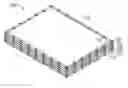
FIG. 1 is an isometric view of an exemplary embodiment of a printed circuit board.
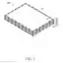
FIG. 2 is a top plan view of the printed circuit board of FIG. 1.
DETAILED DESCRIPTION
The disclosure, including the accompanying drawings in which like references indicate similar elements, is illustrated by way of examples and not by way of limitation. It should be noted that references to “an” or “one” embodiment in this disclosure are not necessarily to the same embodiment, and such references mean at least one.
Referring to FIG. 1, an exemplary embodiment of a printed circuit board 100 includes a first signal layer S1, a first ground layer G1, a second signal layer S2, a power layer P1, a second ground layer G2, and a third signal layer S3. The first signal layer 51, the first ground layer G1, the second signal layer S2, the power layer P1, the second ground layer G2, and the third signal layer S3 are superposed in that order. In other embodiments, the number and the arrangement of the signal layers, the ground layers, and the power layers may be changed according to requirements.
Referring to FIG. 2, a closed trace TR is set along edges of each signal layer and the power layer P1. The width of the trace TR is about 20 mils.
A plurality of vias V1 is defined in the trace TR of the first signal layer S1 at intervals. The distance between two adjacent vias V1 is about 40 mils. Each via V1 extends through the first ground layer G1, the second signal layer S2, the power layer P1, the second ground layer G2, and the third signal layer S3. The diameter of each via V1 is less than the width of the trace TR.
A copper-foil layer is set on the inner wall of each via V1. The copper-foil layer is electrically connected to the traces TR of the first signal layer S1, the second signal layer S2, the power layer P1, and the third signal layer S3. The copper-foil layer is also electrically connected to the first ground layer G1 and the second ground layer G2.
The traces TR, the vias V1, the first ground layer G1, and the second ground layer G2 compose a shielding grid, to prevent electro-magnetic radiation and the fringing effect.
The foregoing description of the exemplary embodiments of the disclosure has been presented only for the purposes of illustration and description and is not intended to be exhaustive or to limit the disclosure to the precise forms disclosed. Many modifications and variations are possible in light of the above everything. The embodiments were chosen and described in order to explain the principles of the disclosure and their practical application so as to enable others of ordinary skill in the art to utilize the disclosure and various embodiments and with various modifications as are suited to the particular use contemplated. Alternative embodiments will become apparent to those of ordinary skills in the art to which the present disclosure pertains without departing from its spirit and scope. Accordingly, the scope of the present disclosure is defined by the appended claims rather than the foregoing description and the exemplary embodiments described therein.
Claims
What is claimed is:1. A printed circuit board comprising a plurality of signal layers, a plurality of ground layers, and a power layer, wherein the signal layers, the ground layers, and the power layer are superposed, a closed trace is set along edges of each of the signal layers and the power layer, a plurality of vias are defined in each trace at intervals, each via extends through the signal layers, the ground layers, and the power layer, each via is electrically connected to the traces of the signal layers and the power layer, and is electrically connected to the ground layers.
2. The printed circuit board of claim 1, wherein the width of each trace is about 20 mils.
3. The printed circuit board of claim 1, wherein the distance between two adjacent vias is about 40 mils.
4. The printed circuit board of claim 3, wherein the diameter of each via is less than the width of each trace.
5. The printed circuit board of claim 1, wherein the plurality of signal layers comprises a first signal layer, a second signal layer, and a third signal layer; the plurality of ground layers comprises a first ground layer and a second ground layer; wherein the first signal layer, the first ground layer, the second signal layer, the power layer, the second ground layer, and the third signal layer are superposed in that order.
Images & Drawings included:

Sources:
- United States Patent and Trademark Office - verify current appl. status at the USPTO↗
Similar patent applications:
- » 20120152592
Method for manufacturing printed circuit board, method for manufacturing printed circuit board assembly sheet, printed circuit board, and printed circuit board assembly sheet - » 20140000941
Method for integrating an electronic component into a printed circuit board or a printed circuit board intermediate product, and printed circuit board or printed circuit board intermediate product - » 20180014403
Substrate for printed circuit board, printed circuit board, and method for producing printed circuit board - » 20210007227
SUBSTRATE FOR PRINTED CIRCUIT BOARD, PRINTED CIRCUIT BOARD, METHOD OF MANUFACTURING SUBSTRATE FOR PRINTED CIRCUIT BOARD, AND COPPER NANO-INK - » 20170099732
Substrate for printed circuit board, printed circuit board, and method for producing substrate for printed circuit board - » 20170290150
Substrate for printed circuit board, printed circuit board, and method for producing substrate for printed circuit board - » 20170347459
Substrate for printed circuit board, printed circuit board, and method for producing substrate for printed circuit board - » 20100326714
Printed circuit board, printed circuit board fabrication method, and electronic device including printed circuit board - » 20170127516
Substrate for printed circuit board, printed circuit board, and method for producing substrate for printed circuit board - » 20180124925
Substrate for printed circuit board, printed circuit board, and method for producing substrate for printed circuit board
Recent applications in this class:
- » 20250294668 2025-09-18
Harness PCB - » 20250247947 2025-07-31
ELECTRONIC DEVICE - » 20250240872 2025-07-24
CIRCUIT BOARD AND DISPLAY APPARATUS - » 20250159793 2025-05-15
ELECTRONIC DEVICE - » 20250113429 2025-04-03
OPTICAL MODULE AND FLEXIBLE PRINTED CIRCUIT BOARD - » 20250016910 2025-01-09
SHIELDABLE CIRCUIT BOARD STRUCTURE - » 20250016909 2025-01-09
PRINTED WIRING BOARD - » 20240431019 2024-12-26
Circuit board local electromagnetic shielding - » 20240397608 2024-11-28
FLEXIBLE PRINTED CIRCUIT BOARD AND METHOD FOR MANUFACTURING THE SAME, AND DISPLAY DEVICE - » 20240389219 2024-11-21
MICRO-GROUND VIAS FOR IMPROVED SIGNAL INTEGRITY FOR HIGH-SPEED SERIAL LINKS
Recent applications for this Assignee:
- » 20140233961 2014-08-21
Optical communication module including optical-electrical signal converters and optical signal generators - » 20140083669 2014-03-27
HEAT SINK - » 20140083669 2014-03-27
HEAT SINK - » 20140063746 2014-03-06
Electronic device with heat dissipation assembly - » 20140061224 2014-03-06
AUTOMATIC VENDING MACHINE - » 20140060914 2014-03-06
Enclosure with shield apparatus - » 20140058727 2014-02-27
MULTIMEDIA RECORDING SYSTEM AND METHOD - » 20140055955 2014-02-27
Fastener - » 20140055322 2014-02-27
DISPLAY SYSTEM AND HEAD-MOUNTED DISPLAY APPARATUS - » 20140054439 2014-02-27
CONTAINER DATA CENTER WITH SUPPORTING APPARATUS