Printed circuit board
US20120048601A1
2012-03-01
12/888,615
2010-09-23
✅ Patent granted
US 8,411,460 B2
2013-04-02
-
-
Tuan T Dinh
Altis Law Group, Inc.
2031-04-23
Abstract:
A printed circuit board includes a power layer, a ground layer, a signal layer, and a backboard. The backboard is arranged below the signal layer opposite to the ground layer. A number of vias are formed from the backboard through the signal layer, and then connected to the ground layer.
Inventors:
- Yong-Zhao HUANG 47 🇨🇳 Shenzhen City, China
- GUANG-FENG OU 16 🇨🇳 Shenzhen City, China
- GUANG-FENG OU 25 🇨🇳 Shenzhen, China
- YONG-ZHAO HUANG 65 🇨🇳 Shenzhen, China
Assignee:
- HON HAI PRECISION INDUSTRY CO., LTD. 12,833 🇹🇼 Tu-Cheng, Taiwan
- HONG FU JIN PRECISION INDUSTRY (SHENZHEN) CO., LTD. 4,225 🇨🇳 Shenzhen City, China
- HON HAI PRECISION INDUSTRY CO., LTD. 10,014 🇹🇼 New Taipei, Taiwan
- HONG FU JIN PRECISION INDUSTRY (ShenZhen) CO., LTD. 2,585 🇨🇳 Shenzhen, China
Applicant:
Interested in similar patents?
Get notified when new applications in this technology area are published.
Classification:
H05K1/0219 » CPC main
Printed circuits; Details; Electrical arrangements not otherwise provided for; Reduction of cross-talk, noise or electromagnetic interference by printed shielding conductors, ground planes or power plane Printed shielding conductors for shielding around or between signal conductors, e.g. coplanar or coaxial printed shielding conductors
H05K2201/09618 » CPC further
Indexing scheme relating to printed circuits covered by; Shape and layout; Shape and layout details of conductors; Conductive through-holes or vias Via fence, i.e. one-dimensional array of vias
H05K2201/09618 » CPC further
Indexing scheme relating to printed circuits covered by; Shape and layout; Shape and layout details of conductors; Conductive through-holes or vias Via fence, i.e. one-dimensional array of vias
H05K1/09 IPC
Printed circuits; Details Use of materials for the conductive, e.g. metallic pattern
H05K1/09 IPC
Printed circuits; Details Use of materials for the conductive, e.g. metallic pattern
H05K1/11 IPC
Printed circuits; Details Printed elements for providing electric connections to or between printed circuits
H05K1/11 IPC
Printed circuits; Details Printed elements for providing electric connections to or between printed circuits
H05K1/14 IPC
Printed circuits; Details Structural association of two or more printed circuits
H05K1/14 IPC
Printed circuits; Details Structural association of two or more printed circuits
Description
BACKGROUND
1. Technical Field
The present disclosure relates to a printed circuit board.
2. Description of Related Art
Electromagnetic interference (EMI) can interfere with the functioning of components of electronic devices. This interference or interruption can occur among components of the same electronic device or may even permeate to other nearby electronic devices. Thus reduction of EMI in electronic devices or components is always a concern for electronic designers or manufacturers. Therefore, there is room for improvement in the art.
BRIEF DESCRIPTION OF THE DRAWINGS
Many aspects of the embodiments can be better understood with reference to the following drawings. The components in the drawings are not necessarily drawn to scale, the emphasis instead being placed upon clearly illustrating the principles of the present embodiments. Moreover, in the drawings, like reference numerals designate corresponding parts throughout the several views.
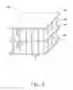
FIG. 1 is a schematic diagram of an exemplary embodiment of a printed circuit board.
FIG. 2 is an isometric diagram of a portion of the printed circuit board of FIG. 1.
DETAILED DESCRIPTION
The disclosure, including the drawings, is illustrated by way of example and not by limitation. It should be noted that references to “an” or “one” embodiment in this disclosure are not necessarily to the same embodiment, and such references mean at least one.
Referring to FIGS. 1 and 2, an embodiment of a printed circuit board (PCB) 100 includes four layers as an example. The PCB 100 includes a first signal layer 10, a power layer 20, a ground layer 30, a second signal layer 40, and a backboard 50. Dielectric is filled between the ground layer 30 and the second signal layer 40. Dielectric is filled between the second signal layer 40 and the backboard 50. A plurality of vias 60 is equidistantly arranged along sides of the backboard 50. The vias 60 extend through the second signal layer 40, and then are connected to the ground layer 30. An electronic element, such as a central processing unit (CPU) 12 is set on the first signal layer 10, opposite to the power layer 20.
In one embodiment, the backboard 50 is made of high-strength metal, such as steel or iron. Large thickness and small dielectric constant Er of dielectric between the second signal layer 40 and the backboard 50 can be selected, to make characteristic resistance of the signal lines of the second signal layer 40 consistent with characteristic resistance of the signal lines of the first signal layer 10. The backboard 50 may only partially overlap the second signal layer 40, which centralizes high speed signal lines and clock lines of the second signal layer 40 of the PCB 100, to save cost. The number of the vias 60 can be increased or through holes can be defined in the backboard 50, to cool the second signal layer 40 of the PCB 100.
In an alternative embodiment, to gain better shielding effectiveness, the via distance S between two adjacent vias 60 is less than a twentieth of the wave length of the radiated wave having the highest frequency transmitted by the PCB 100.
The wave length L of the radiated wave having the highest frequency can be calculated by the formula: L=V/f, where “V” stands for the transmission speed of signals flowing through the signal lines, and “f” stands for the highest frequency of the radiated wave. The speed V of the radiated wave having the highest frequency can be calculated by the formula: V=C/Er1/2, where “C” stands for the speed of light, “Er” stands for the dielectric constant of the dielectric. According to the formula that wave length equals speed divided by frequency, the via distance S can be described as: S<C/(20*f*Er1/2).
For example, when the frequency f=50 gigahertz of the radiated wave having the highest frequency, and the Er=4.0, according to the above formulas the via distance S<1.5 millimeters of the backboard 50 calculated.
The vias 60 are equidistantly arranged along sides of the backboard 50, and extend through the second signal layer 40 and then are connected to the ground layer 30, thereby making the backboard 50, the second signal layer 40, and the ground layer 30 form a Faraday cage. As is well known, a Faraday cage can effectively block interference from external electrical fields.
The backboard 50 reinforces strength of the PCB 100. Thus, thickness of each layer of the PCB 100 can be greatly reduced, which reduces electromagnetic interference (EMI) related to signals passing through the first and second signal layers 10 and 40.
The backboard 50 increases strength of the PCB 100, and the vias 60 are equidistantly arranged along sides of the backboard 50 to form a Faraday cage. Therefore, EMI of the PCB 100 can be effectively minimized.
It is to be understood, however, that even though numerous characteristics and advantages of the present disclosure have been set forth in the foregoing description, together with details of the structure and function of the disclosure, the disclosure is illustrative only, and changes may be made in detail, especially in matters of shape, size, and arrangement of parts within the principles of the disclosure to the full extent indicated by the broad general meaning of the terms in which the appended claims are expressed.
Claims
What is claimed is:1. A printed circuit board (PCB) comprising:
a ground layer;
a first signal layer; and
a backboard;
wherein the backboard is arranged below the first signal layer, a plurality of vias is formed on the backboard, the vias extend through the first signal layer and then are connected to the ground layer.
2. The PCB of claim 1, further comprising a second signal layer and a power layer, wherein the power layer is sandwiched between the second signal layer and the ground layer, the first signal layer is arranged below the ground layer opposite to the power layer, the backboard is arranged below the first signal layer opposite to the ground layer.
3. The PCB of claim 2, wherein dielectric is filled between the ground layer and the first signal layer, and dielectric is filled between the first signal layer and the backboard.
4. The PCB of claim 1, wherein the plurality of vias is equidistantly arranged along sides of the backboard.
5. The PCB of claim 1, wherein the backboard is made of high strength metal material.
6. The PCB of claim 5, wherein the metal material is steel or iron.
Images & Drawings included:
Sources:
- United States Patent and Trademark Office - verify current appl. status at the USPTO↗
Similar patent applications:
- » 20120152592
Method for manufacturing printed circuit board, method for manufacturing printed circuit board assembly sheet, printed circuit board, and printed circuit board assembly sheet - » 20140000941
Method for integrating an electronic component into a printed circuit board or a printed circuit board intermediate product, and printed circuit board or printed circuit board intermediate product - » 20180014403
Substrate for printed circuit board, printed circuit board, and method for producing printed circuit board - » 20210007227
SUBSTRATE FOR PRINTED CIRCUIT BOARD, PRINTED CIRCUIT BOARD, METHOD OF MANUFACTURING SUBSTRATE FOR PRINTED CIRCUIT BOARD, AND COPPER NANO-INK - » 20170099732
Substrate for printed circuit board, printed circuit board, and method for producing substrate for printed circuit board - » 20170290150
Substrate for printed circuit board, printed circuit board, and method for producing substrate for printed circuit board - » 20170347459
Substrate for printed circuit board, printed circuit board, and method for producing substrate for printed circuit board - » 20100326714
Printed circuit board, printed circuit board fabrication method, and electronic device including printed circuit board - » 20170127516
Substrate for printed circuit board, printed circuit board, and method for producing substrate for printed circuit board - » 20180124925
Substrate for printed circuit board, printed circuit board, and method for producing substrate for printed circuit board
Recent applications in this class:
- » 20250261301 2025-08-14
MANAGING CROSSTALK FOR HIGH DATA RATE INTERFACES - » 20250247949 2025-07-31
WEARABLE DEVICE INCLUDING STRUCTURE FOR PREVENTING NOISE CAUSED BY STATIC ELECTRICITY - » 20250247948 2025-07-31
INPUT/OUTPUT APPARATUS - » 20250113430 2025-04-03
TECHNOLOGIES FOR REDUCING THE IMPACT OF RADIOFREQUENCY INTERFERENCE ON A CIRCUIT BOARD - » 20250056710 2025-02-13
WIRING SUBSTRATES AND ELECTRONIC APPARATUSES - » 20250024586 2025-01-16
ENHANCED MICROSTRIP TRACE - » 20240414839 2024-12-12
MANUFACTURING METHOD OF PRINTED CIRCUIT BOARD - » 20240397609 2024-11-28
WIRING CIRCUIT BOARD AND METHOD OF PRODUCING THE WIRING CIRCUIT BOARD - » 20240373546 2024-11-07
Flexible Hybrid Interconnect Circuits - » 20240292516 2024-08-29
WIRING BOARD AND ELECTRONIC DEVICE
Recent applications for this Assignee:
- » 20250218287 2025-07-03
METHOD OF GENERATING AND PROMPTING TRAFFIC INFORMATION, AND ROADSIDE DEVICE THEREOF - » 20250178535 2025-06-05
METHOD FOR CONSTRUCTING 3D PANORAMIC VIEW MODEL, VEHICLE-MOUNTED DEVICE, AND STORAGE MEDIUM - » 20250074444 2025-03-06
METHOD FOR EARLY WARNING A BLIND AREA, ELECTRONIC DEVICE AND STORAGE MEDIUM - » 20240416754 2024-12-19
DISPLAY CONTROL DEVICE, DISPLAY EQUIPMENT, AND VEHICLE EMPLOYING DEVICE - » 20240411051 2024-12-12
Light-emitting device array and optical transceiver system having the same - » 20240324114 2024-09-26
DISPLAY CONTROL DEVICE AND VEHICLE EMPLOYING DEVICE - » 20240295957 2024-09-05
METHOD FOR CONTROLLING ELECTRONIC DEVICE, ELECTRONIC DEVICE AND COMPUTER STROAGE MEDIUM EMPLOYING METHOD - » 20240257357 2024-08-01
METHOD FOR DETECTING OBSTACLES, ELECTRONIC DEVICE, AND STORAGE MEDIUM - » 20240203133 2024-06-20
LANE LINE RECOGNITION METHOD, ELECTRONIC DEVICE AND STORAGE MEDIUM - » 20240194999 2024-06-13
Robot using limiting device for locking battery