Semiconductor package
US20120049360A1
2012-03-01
12/872,644
2010-08-31
✅ Patent granted
US 8,368,216 B2
2013-02-05
-
-
A O Williams
McCracken & Frank LLC
2031-01-20
Abstract:
The present invention relates to a semiconductor package and a method for making the same. The semiconductor package includes at least one first layer chip, a plurality of first metal bumps, at least one second layer chip and a package body. The first layer chip includes a first active surface and a plurality of first signal coupling pads. The first signal coupling pads are disposed adjacent to the first active surface. The first metal bumps are disposed on the first active surface of the first layer chip. The second layer chip is electrically connected to the first layer chip, and includes a second active surface and a plurality of second signal coupling pads. The second active surface faces the first active surface of the first layer chip. The second signal coupling pads are disposed adjacent to the second active surface, and capacitively coupled to the first signal coupling pads of the first layer chip, so as to provide proximity communication between the first layer chip and the second layer chip. The package body encapsulates the first layer chip, the first metal bumps and the second layer chip, and the first metal bumps are partially exposed. Whereby, the bonding strength between the first layer chip and the second layer chip is increased because of the package body, so the yield of the semiconductor package is increased.
Inventors:
- Yi-Shao LAI 8 🇹🇼 Kaohsiung, Taiwan
- Tsung-Yueh TSAI 40 🇹🇼 Kaohsiung, Taiwan
- Ming-Hsiang CHENG 15 🇹🇼 Kaohsiung, Taiwan
- Ming-Kun Chen 9 🇹🇼 Kaohsiung, Taiwan
- Hsiao-Chuan Chang 17 🇹🇼 Kaohsiung, Taiwan
Assignee:
- ADVANCED SEMICONDUCTOR ENGINEERING, INC. 1,972 🇹🇼 Kaohsiung, Taiwan
Applicant:
Interested in similar patents?
Get notified when new applications in this technology area are published.
Classification:
H01L21/6835 » CPC main
Processes or apparatus adapted for the manufacture or treatment of semiconductor or solid state devices or of parts thereof; Apparatus specially adapted for handling semiconductor or electric solid state devices during manufacture or treatment thereof; Apparatus specially adapted for handling wafers during manufacture or treatment of semiconductor or electric solid state devices or components ; Apparatus not specifically provided for elsewhere for supporting or gripping using temporarily an auxiliary support
H01L21/568 » CPC further
Processes or apparatus adapted for the manufacture or treatment of semiconductor or solid state devices or of parts thereof; Manufacture or treatment of semiconductor devices or of parts thereof the devices having at least one potential-jump barrier or surface barrier, e.g. PN junction, depletion layer or carrier concentration layer; Assembly of semiconductor devices using processes or apparatus not provided for in a single one of the subgroups - , e.g. sealing of a cap to a base of a container; Encapsulations, e.g. encapsulation layers, coatings Temporary substrate used as encapsulation process aid
H01L25/0652 » CPC further
Assemblies consisting of a plurality of individual semiconductor or other solid state devices ; Multistep manufacturing processes thereof all the devices being of a type provided for in the same subgroup of groups - , e.g. assemblies of rectifier diodes the devices not having separate containers the devices being of a type provided for in group the devices being arranged next and on each other, i.e. mixed assemblies
H01L25/50 » CPC further
Assemblies consisting of a plurality of individual semiconductor or other solid state devices ; Multistep manufacturing processes thereof Multistep manufacturing processes of assemblies consisting of devices, each device being of a type provided for in group or
H01L21/563 » CPC further
Processes or apparatus adapted for the manufacture or treatment of semiconductor or solid state devices or of parts thereof; Manufacture or treatment of semiconductor devices or of parts thereof the devices having at least one potential-jump barrier or surface barrier, e.g. PN junction, depletion layer or carrier concentration layer; Assembly of semiconductor devices using processes or apparatus not provided for in a single one of the subgroups - , e.g. sealing of a cap to a base of a container; Encapsulations, e.g. encapsulation layers, coatings Encapsulation of active face of flip-chip device, e.g. underfilling or underencapsulation of flip-chip, encapsulation preform on chip or mounting substrate
H01L23/3114 » CPC further
Details of semiconductor or other solid state devices; Encapsulations, e.g. encapsulating layers, coatings, e.g. for protection characterised by the arrangement or shape the device being completely enclosed the device being a chip scale package, e.g. CSP
H01L24/27 » CPC further
Arrangements for connecting or disconnecting semiconductor or solid-state bodies; Methods or apparatus related thereto; Means for bonding being attached to, or being formed on, the surface to be connected, e.g. chip-to-package, die-attach, "first-level" interconnects; Manufacturing methods related thereto; Layer connectors, e.g. plate connectors, solder or adhesive layers; Manufacturing methods related thereto Manufacturing methods
H01L2224/1184 » CPC further
Indexing scheme for arrangements for connecting or disconnecting semiconductor or solid-state bodies and methods related thereto as covered by; Means for bonding being attached to, or being formed on, the surface to be connected, e.g. chip-to-package, die-attach, "first-level" interconnects; Manufacturing methods related thereto; Bump connectors; Manufacturing methods related thereto; Manufacturing methods; Post-treatment of the bump connector; Reworking, e.g. shaping involving a mechanical process, e.g. planarising the bump connector
H01L2224/2784 » CPC further
Indexing scheme for arrangements for connecting or disconnecting semiconductor or solid-state bodies and methods related thereto as covered by; Means for bonding being attached to, or being formed on, the surface to be connected, e.g. chip-to-package, die-attach, "first-level" interconnects; Manufacturing methods related thereto; Layer connectors, e.g. plate connectors, solder or adhesive layers; Manufacturing methods related thereto; Manufacturing methods; Post-treatment of the layer connector; Reworking, e.g. shaping involving a mechanical process, e.g. planarising the layer connector
H01L2224/73104 » CPC further
Indexing scheme for arrangements for connecting or disconnecting semiconductor or solid-state bodies and methods related thereto as covered by; Means for bonding being of different types provided for in two or more of groups; Location prior to the connecting process on the same surface; Bump and layer connectors the bump connector being embedded into the layer connector
H01L2224/73204 » CPC further
Indexing scheme for arrangements for connecting or disconnecting semiconductor or solid-state bodies and methods related thereto as covered by; Means for bonding being of different types provided for in two or more of groups; Location after the connecting process on the same surface; Bump and layer connectors the bump connector being embedded into the layer connector
H01L2224/81005 » CPC further
Indexing scheme for arrangements for connecting or disconnecting semiconductor or solid-state bodies and methods related thereto as covered by; Methods for connecting semiconductor or other solid state bodies using means for bonding being attached to, or being formed on, the surface to be connected using a bump connector involving a temporary auxiliary member not forming part of the bonding apparatus being a temporary or sacrificial substrate
H01L2224/81801 » CPC further
Indexing scheme for arrangements for connecting or disconnecting semiconductor or solid-state bodies and methods related thereto as covered by; Methods for connecting semiconductor or other solid state bodies using means for bonding being attached to, or being formed on, the surface to be connected using a bump connector; Bonding techniques Soldering or alloying
H01L2224/8185 » CPC further
Indexing scheme for arrangements for connecting or disconnecting semiconductor or solid-state bodies and methods related thereto as covered by; Methods for connecting semiconductor or other solid state bodies using means for bonding being attached to, or being formed on, the surface to be connected using a bump connector; Bonding techniques using a polymer adhesive, e.g. an adhesive based on silicone, epoxy, polyimide, polyester
H01L2224/831 » CPC further
Indexing scheme for arrangements for connecting or disconnecting semiconductor or solid-state bodies and methods related thereto as covered by; Methods for connecting semiconductor or other solid state bodies using means for bonding being attached to, or being formed on, the surface to be connected using a layer connector the layer connector being supplied to the parts to be connected in the bonding apparatus
H01L2225/06513 » CPC further
Details relating to assemblies covered by the group but not provided for in its subgroups; All the devices being of a type provided for in the same subgroup of groups - the devices not having separate containers the devices being of a type provided for in group; Stacked arrangements of devices Bump or bump-like direct electrical connections between devices, e.g. flip-chip connection, solder bumps
H01L2924/15311 » CPC further
Indexing scheme for arrangements or methods for connecting or disconnecting semiconductor or solid-state bodies as covered by; Details of package parts other than the semiconductor or other solid state devices to be connected; Die mounting substrate; Connection portion the connection portion being formed only on the surface of the substrate opposite to the die mounting surface being a ball array, e.g. BGA
H01L2924/15321 » CPC further
Indexing scheme for arrangements or methods for connecting or disconnecting semiconductor or solid-state bodies as covered by; Details of package parts other than the semiconductor or other solid state devices to be connected; Die mounting substrate; Connection portion the connection portion being formed on the die mounting surface of the substrate being a ball array, e.g. BGA
H01L2924/014 » CPC further
Indexing scheme for arrangements or methods for connecting or disconnecting semiconductor or solid-state bodies as covered by; Alloys Solder alloys
H01L23/538 IPC
Details of semiconductor or other solid state devices; Arrangements for conducting electric current within the device in operation from one component to another, i.e. interconnections, e.g. wires, lead frames the interconnection structure between a plurality of semiconductor chips being formed on, or in, insulating substrates
H01L21/60 IPC
Processes or apparatus adapted for the manufacture or treatment of semiconductor or solid state devices or of parts thereof; Manufacture or treatment of semiconductor devices or of parts thereof the devices having at least one potential-jump barrier or surface barrier, e.g. PN junction, depletion layer or carrier concentration layer; Assembly of semiconductor devices using processes or apparatus not provided for in a single one of the subgroups - , e.g. sealing of a cap to a base of a container Attaching or detaching leads or other conductive members, to be used for carrying current to or from the device in operation
H01L23/488 IPC
Details of semiconductor or other solid state devices; Arrangements for conducting electric current to or from the solid state body in operation, e.g. leads, terminal arrangements ; Selection of materials therefor consisting of soldered constructions
Description
BACKGROUND OF THE INVENTION
1. Field of the Invention
The present invention relates to a semiconductor package and a method for making the same, and more particularly to a semiconductor package having signal coupling pads and a method for making the same.
2. Description of the Related Art
A new technique referred to as “proximity communication” overcomes the limitations of conductive electrical interconnections by using capacitive coupling to provide communications between two chips. This technique provides higher input/output pads densities than traditional wire-bonding and flip-chip bonding input/output pads (about 100 times greater). To achieve proximity communication, the input/output pads disposed on an active surface of each chip are placed face-to-face with extreme accuracy, and the bonding strength between two chips is weak, so the two chips are separated from each other easily during being mounted to the substrate.
Therefore, it is necessary to provide a semiconductor package and a method for making the same to solve the above problems.
SUMMARY OF THE INVENTION
The present invention is directed to a semiconductor package. The semiconductor package comprises at least one first layer chip, a plurality of first metal bumps, at least one second layer chip and a package body. The first layer chip comprises a first active surface and a plurality of first signal coupling pads. The first signal coupling pads are disposed adjacent to the first active surface. The first metal bumps are disposed on the first active surface of the first layer chip. The second layer chip is electrically connected to the first layer chip, and comprises a second active surface and a plurality of second signal coupling pads. The second active surface faces the first active surface of the first layer chip. The second signal coupling pads are disposed adjacent to the second active surface, and capacitively coupled to the first signal coupling pads of the first layer chip, so as to provide proximity communication between the first layer chip and the second layer chip. The package body encapsulates the first layer chip, the first metal bumps and the second layer chip, and the first metal bumps are partially exposed.
The present invention is further directed to a method for making a semiconductor package. The method comprises the following steps: (a) providing a carrier and a release tape, wherein the release tape is disposed on the carrier; (b) providing at least one first layer chip and a plurality of first metal bumps, wherein the first layer chip has a first active surface, a first back surface and a plurality of first signal coupling pads, the first signal coupling pads are disposed adjacent to the first active surface, and the first metal bumps are disposed on the first active surface of the first layer chip; (c) disposing the first layer chip on the release tape, wherein the first back surface of the first layer chip contacts the release tape; (d) attaching and electrically connecting at least one second layer chip to the first layer chip, wherein the second layer chip has a second active surface and a plurality of second signal coupling pads, the second active surface faces the first active surface of the first layer chip, the second signal coupling pads are disposed adjacent to the second active surface, and capacitively coupled to the first signal coupling pads of the first layer chip, so as to provide proximity communication between the first layer chip and the second layer chip; (e) forming a package body to encapsulate the first layer chip, the first metal bumps and the second layer chip; (f) removing part of the package body so as to expose at least a portion of each of the first metal bumps; and (g) removing the release tape and the carrier.
Whereby, the bonding strength between the first layer chip and the second layer chip is increased because of the package body, so the yield of the semiconductor package is increased.
BRIEF DESCRIPTION OF THE DRAWINGS
FIGS. 1 to 8 are schematic views of a method for making a semiconductor package according to the present invention.
DETAILED DESCRIPTION OF THE INVENTION
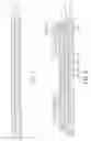
FIGS. 1 to 8 show schematic views of a method for making a semiconductor package according to the present invention. As shown in FIG. 1, a carrier 11 and a release tape 12 are provided. The release tape 12 is disposed on the carrier 11. In the embodiment, the release tape 12 is a thermal release tape.
As shown in FIG. 2, at least one first layer chip 13 and a plurality of first metal bumps 14 are provided. The first layer chip 13 has a first active surface 131, a first back surface 132 and a plurality of first signal coupling pads 133. The first signal coupling pads 133 are disposed adjacent to the first active surface 131. The first metal bumps 14 are disposed on the first active surface 131 of the first layer chip 13. In the embodiment, the first layer chip 13 further comprises a plurality of first layer chip pads 134 disposed adjacent to the first active surface 131. The number of the first layer chip 13 is two, the first metal bumps 14 are connected to one end of each first layer chip 13, and the first signal coupling pads 133 are disposed at another end of each first layer chip 13.
The first layer chip 13 is disposed on the release tape 12. The first back surface 132 of the first layer chip 13 contacts the release tape 12. Preferably, in the embodiment, a metal frame 15 is disposed on the release tape 12. As shown in FIG. 3, the metal frame 15 surrounds the first layer chip 13 and has a portion located between the two first layer chips 13, and the metal frame 15 does not contact the first layer chip 13. Note that the metal frame 15 is not an essential aspect of the present invention.
As shown in FIG. 4, at least one second layer chip 17 is attached and electrically connected to the first layer chip 13. The second layer chip 17 has a second active surface 171 and a plurality of second signal coupling pads 172. The second active surface 171 faces the first active surface 131 of the first layer chip 13. The second signal coupling pads 172 are disposed adjacent to the second active surface 171, and capacitively coupled to the first signal coupling pads 133 of the first layer chip 13, so as to provide proximity communication between the first layer chip 13 and the second layer chip 17. In the embodiment, the second layer chip 17 further comprises a plurality of second layer chip pads 173 disposed adjacent to the second active surface 171, the first layer chip pads 134 are connected to the second layer chip pads 173 by a plurality of conductive element 18. The conductive element 18 may be a micro-solder ball, an anisotropic conductive film (ACF) or an anisotropic conductive paste (ACP). The height of the conductive element 18 is less than about 20 μm.
As shown in FIG. 5, a package body 19 is formed to encapsulate the first layer chip 13, the first metal bumps 14 and the second layer chip 17. The package body 19 may be formed by transfer molding a molding compound through a system of runners and gates in a mold. Alternatively, the package body 19 may be formed by a dispensing process. In the embodiment, an underfill 21 is formed between the first layer chip 13 and the second layer chip 17 before forming the package body 19. As shown in FIG. 6, part of the package body 19 is removed so as to expose at least a portion of each of the first metal bumps 14. That is, each of the first metal bumps 14 has at least a portion exposed from the package body 19. As shown in FIG. 7, the release tape 12 and the carrier 11 are removed, and the semiconductor package 1 is formed.
In other embodiment, as shown in FIG. 8, a substrate 22 and a solder paste 23 are further provided. The substrate 22 has a receiving surface 221, and the solder paste 23 is disposed on the receiving surface 221 of the substrate 22. A bonding process is further conducted. The first active surface 131 of the first layer chip 13 faces the receiving surface 221 of the substrate 22, and the first metal bumps 14 contact the solder paste 23.
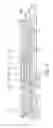
FIG. 7 shows a cross-sectional view of a semiconductor package according to the present invention. The semiconductor package 1 comprises at least one first layer chip 13, a plurality of first metal bumps 14, at least one second layer chip 17 and a package body 19. In the embodiment, the semiconductor package 1 further comprises an underfill 21, and a metal frame 15.
The first layer chip 13 comprises a first active surface 131 and a plurality of first signal coupling pads 133. The first signal coupling pads 133 are disposed adjacent to the first active surface 131. In the embodiment, the first layer chip 13 further comprises a plurality of first layer chip pads 134 disposed adjacent to the first active surface 131.
The first metal bumps 14 are disposed on the first active surface 131 of the first layer chip 13. In the embodiment, the number of the first layer chip 13 is two, the first metal bumps 14 are connected to one end of each first layer chip 13, and the first signal coupling pads 133 are disposed at another end of each first layer chip 13.
The second layer chip 17 is electrically connected to the first layer chip 13, and comprises a second active surface 171 and a plurality of second signal coupling pads 172. The second active surface 171 faces the first active surface 131 of the first layer chip 13. The second signal coupling pads 172 are disposed adjacent to the second active surface 171, and capacitively coupled to the first signal coupling pads 133 of the first layer chip 13, so as to provide proximity communication between the first layer chip 13 and the second layer chip 17. In the embodiment, the second layer chip 17 further comprises a plurality of second layer chip pads 173 disposed adjacent to the second active surface 171, the first layer chip pads 134 are connected to the second layer chip pads 173 by a plurality of conductive element 18. The conductive element 18 may be a micro-solder ball, an anisotropic conductive film (ACF) or an anisotropic conductive paste (ACP). The height of the conductive element 18 is less than about 20 μm.
The package body 19 encapsulates the first layer chip 13, the first metal bumps 14, the second layer chip 17 and the metal frame 15. Each of the first metal bumps 14 has at least a portion exposed from the package body 19. In the embodiment, a plurality of exposed surfaces 141 of the first metal bumps 14 are coplanar with a first surface 191 of the package body 19, and a first back surface 132 of the first layer chip 13 is coplanar with a second surface 192 of the package body 19.
The underfill 21 is disposed between the first layer chip 13 and the second layer chip 17. The metal frame 15 surrounds the first layer chip 13 and between the two first layer chips 13. The metal frame 15 does not contact the first layer chip 13. The metal frame 15 is embedded in the package body 19.
In other embodiment, as shown in FIG. 8, the semiconductor package 1 may further comprise a substrate 22 and a solder paste 23. The substrate 22 has a receiving surface 221, the solder paste 23 is disposed between the receiving surface 221 of the substrate 22 and the first metal bumps 14, the first layer chip 13 is attached and electrically connected to the receiving surface 221 of the substrate 22 by the first metal bumps 14 and the solder paste 23.
Whereby, the bonding strength between the first layer chip 13 and the second layer chip 17 is increased because of the package body 19, so the yield of the semiconductor package 1 is increased.
It should be noted that the first layer chip 13 and the second layer chip 17 communicate with each other through proximity communication between the first signal coupling pads 133 and the second signal coupling pads 172, instead of direct electrical connections; however, electrical power or ground is transmitted between the first layer chip 13 and the second layer chip 17 through direct electrical connections (the conductive element 18).
In order to achieve the function of proximity communication, part of the first layer chip 13 and the second layer chip 17 are placed face-to-face in a manner that aligns the transmitter circuit with the receiver circuit in extremely close proximity, for example, with only microns of separation between them. The signals between the transmitter circuit and the receiver circuit may be transmitted by inductive or capacitive coupling with low overall communication cost.
Take transmission by capacitive coupling for example. The first signal coupling pads 133 of the first layer chip 13 and the second signal coupling pads 172 of the second layer chip 17 are aligned with each other. Since the first signal coupling pads 133 and the second signal coupling pads 172 are not in physical contact with each other, there are capacitances between the first signal coupling pads 133 of the first layer chip 13 and the second signal coupling pads 172 of the second layer chip 17. It is this capacitive coupling that provides signal paths between the first layer chip 13 and the second layer chip 17. Changes in the electrical potential of the first signal coupling pads 133 of the first layer chip 13 cause corresponding changes in the electrical potential of the corresponding second signal coupling pads 172 of the second layer chip 17. Suitable drivers of the transmitter circuit and sensing circuits of the receiver circuit in the first layer chip 13 and the second layer chip 17 make communication through this small capacitance possible.
While several embodiments of the present invention have been illustrated and described, various modifications and improvements can be made by those skilled in the art. The embodiments of the present invention are therefore described in an illustrative but not restrictive sense. It is intended that the present invention should not be limited to the particular forms as illustrated, and that all modifications which maintain the spirit and scope of the present invention are within the scope defined by the appended claims.
Claims
What is claimed is:1. A semiconductor package, comprising:
at least one first layer chip, comprising:
a first active surface; and
a plurality of first signal coupling pads, disposed adjacent to the first active surface;
a plurality of first metal bumps, disposed on the first active surface of the first layer chip;
at least one second layer chip, disposed on the first active surface and electrically connected to the first layer chip, comprising:
a second active surface, facing the first active surface of the first layer chip; and
a plurality of second signal coupling pads, disposed adjacent to the second active surface, and capacitively coupled to the first signal coupling pads of the first layer chip, so as to provide proximity communication between the first layer chip and the second layer chip; and
a package body, encapsulating the first layer chip, the first metal bumps and the second layer chip, wherein each of the first metal bumps has at least a portion exposed from the package body.
2. The semiconductor package as claimed in claim 1, wherein the first layer chip further comprises a plurality of first layer chip pads disposed adjacent to the first active surface, the second layer chip further comprises a plurality of second layer chip pads disposed adjacent to the second active surface, the first layer chip pads are connected to the second layer chip pads by a plurality of conductive element.
3. The semiconductor package as claimed in claim 2, wherein the conductive element is a micro-solder ball, an anisotropic conductive film (ACF) or an anisotropic conductive paste (ACP).
4. The semiconductor package as claimed in claim 2, wherein the height of the conductive element is less than about 20 μm.
5. The semiconductor package as claimed in claim 1, wherein the number of the first layer chip is two, the first metal bumps are connected to one end of each first layer chip, and the first signal coupling pads are disposed at another end of each first layer chip.
6. The semiconductor package as claimed in claim 1, wherein a plurality of exposed surfaces of the first metal bumps are coplanar with a first surface of the package body.
7. The semiconductor package as claimed in claim 1, wherein a first back surface of the first layer chip is coplanar with a second surface of the package body.
8. The semiconductor package as claimed in claim 1, further comprising an underfill disposed between the first layer chip and the second layer chip.
9. The semiconductor package as claimed in claim 1, further comprising a metal frame surrounding the first layer chip, and the metal frame does not contact the first layer chip.
10. The semiconductor package as claimed in claim 1, further comprising a substrate and a solder paste, wherein the substrate has a receiving surface, the solder paste is disposed between the receiving surface of the substrate and the first metal bumps, the first layer chip is attached and electrically connected to the receiving surface of the substrate by the first metal bumps and the solder paste.
11. A method for making a semiconductor package, comprising:
(a) providing a carrier and a release tape, wherein the release tape is disposed on the carrier;
(b) providing at least one first layer chip having a first active surface, a first back surface, a plurality of first metal bumps, and a plurality of first signal coupling pads, wherein the first signal coupling pads are disposed adjacent to the first active surface, and the first metal bumps are disposed on the first active surface of the first layer chip;
(c) disposing the first layer chip on the release tape, wherein the first back surface of the first layer chip contacts the release tape;
(d) attaching and electrically connecting at least one second layer chip to the first layer chip, wherein the second layer chip has a second active surface and a plurality of second signal coupling pads, the second active surface faces the first active surface of the first layer chip, the second signal coupling pads are disposed adjacent to the second active surface, and capacitively coupled to the first signal coupling pads of the first layer chip, so as to provide proximity communication between the first layer chip and the second layer chip;
(e) forming a package body to encapsulate the first layer chip, the first metal bumps and the second layer chip;
(f) removing part of the package body so as to expose at least a portion of each of the first metal bumps; and
(g) removing the release tape and the carrier.
12. The method as claimed in claim 11, wherein in step (a), the release tape is a thermal release tape.
13. The method as claimed in claim 11, wherein in step (b), the first layer chip further comprises a plurality of first layer chip pads disposed adjacent to the first active surface, in step (d), the second layer chip further comprises a plurality of second layer chip pads disposed adjacent to the second active surface, the first layer chip pads are connected to the second layer chip pads by a plurality of conductive element.
14. The method as claimed in claim 11, wherein in step (b), the number of the first layer chip is two, the first metal bumps are connected to one end of each first layer chip, and the first signal coupling pads are disposed at another end of each first layer chip.
15. The method as claimed in claim 11, further comprising a step of disposing a metal frame on the release tape in step (c), wherein the metal frame surrounds the first layer chip.
16. The method as claimed in claim 11, further comprising a step of forming an underfill between the first layer chip and the second layer chip before step (e).
17. The method as claimed in claim 11, further comprising a step of disposing a metal frame on the release tape in step (c), wherein the metal frame does not contact the first layer chip.
18. The method as claimed in claim 11, wherein after step (g) further comprises:
(h) providing a substrate and a solder paste, wherein the substrate has a receiving surface, and the solder paste is disposed on the receiving surface of the substrate; and
(i) conducting a bonding process, wherein the first active surface of the first layer chip faces the receiving surface of the substrate, and the first metal bumps contact the solder paste.
Images & Drawings included:


Sources:
- United States Patent and Trademark Office - verify current appl. status at the USPTO↗
Similar patent applications:
- » 20210343617
Semiconductor devices including a lower semiconductor package, an upper semiconductor package on the lower semiconductor package, and a connection pattern between the lower semiconductor package and the upper semiconductor package - » 20230207416
Semiconductor devices including a lower semiconductor package, an upper semiconductor package on the lower semiconductor package, and a connection pattern between the lower semiconductor package and the upper semiconductor package - » 20110079890
Semiconductor package, semiconductor package structure including the semiconductor package, and mobile phone including the semiconductor package structure - » 20250149527
SEMICONDUCTOR PACKAGE, SEMICONDUCTOR PACKAGE INTERMEDIATE, REDISTRIBUTION LAYER CHIP, REDISTRIBUTION LAYER CHIP INTERMEDIATE, METHOD OF MANUFACTURING SEMICONDUCTOR PACKAGE, AND METHOD OF MANUFACTURING SEMICONDUCTOR PACKAGE INTERMEDIATE - » 20100213620
Manufacturing method of substrate for a semiconductor package, manufacturing method of semiconductor package, substrate for a semiconductor package and semiconductor package - » 20130309818
Manufacturing method of substrate for a semiconductor package, manufacturing method of semiconductor package, substrate for a semiconductor package and semiconductor package - » 20120064666
MANUFACTURING METHOD OF SUBSTRATE FOR A SEMICONDUCTOR PACKAGE, MANUFACTURING METHOD OF SEMICONDUCTOR PACKAGE, SUBSTRATE FOR A SEMICONDUCTOR PACKAGE AND SEMICONDUCTOR PACKAGE - » 20190267315
Method of manufacturing semiconductor package substrate and semiconductor package substrate manufactured using the method, and method of manufacturing semiconductor package and semiconductor package manufactured using the method - » 20110014748
Semiconductor packages, stacked semiconductor packages, and methods of manufacturing the semiconductor packages and the stacked semiconductor packages - » 20080157394
Semiconductor packages, stacked semiconductor packages, and methods of manufacturing the semiconductor packages and the stacked semiconductor packages
Recent applications in this class:
- » 20250293073 2025-09-18
RECLAIMABLE DONOR SUBSTRATES FOR USE IN PREPARING MULTIPLE SILICON-ON-INSULATOR STRUCTURES - » 20250285904 2025-09-11
HETEROGENEOUS INTEGRATION OF COMPONENTS ONTO COMPACT DEVICES USING MOIRÉ BASED METROLOGY AND VACUUM BASED PICK-AND-PLACE - » 20250273501 2025-08-28
TEMPORARY PROTECTION FILM FOR PRODUCTION OF SEMICONDUCTOR DEVICE AND PRODUCTION METHOD FOR SEMICONDUCTOR DEVICE - » 20250259877 2025-08-14
SEMICONDUCTOR DEVICE AND MANUFACTURING METHOD OF SEMICONDUCTOR DEVICE - » 20250246475 2025-07-31
CARRIER SUBSTRATE AND METHOD OF MANUFACTURING SEMICONDUCTOR PACKAGE USING THE SAME - » 20250239477 2025-07-24
LIGHT-EMITTING ELEMENT ARRAY SUBSTRATE AND METHOD FOR MANUFACTURING LIGHT-EMITTING ELEMENT ARRAY SUBSTRATE - » 20250233002 2025-07-17
MATERIAL FOR POSITIONAL ERROR COMPENSATION IN ASSEMBLY OF DISCRETE COMPONENTS - » 20250218850 2025-07-03
SEMICONDUCTOR DEVICE ARRANGEMENT - » 20250218849 2025-07-03
WAFER BONDING APPARATUS - » 20250218848 2025-07-03
METHOD OF MANUFACTURING DISPLAY DEVICE
Recent applications for this Assignee:
- » 20250294670 2025-09-18
ELECTRONIC DEVICE - » 20250293221 2025-09-18
ELECTRONIC DEVICE - » 20250285950 2025-09-11
SEMICONDUCTOR DEVICE PACKAGE - » 20250282612 2025-09-11
PACKAGE STRUCTURE - » 20250273638 2025-08-28
SEMICONDUCTOR DEVICE PACKAGE INCLUDING STRESS BUFFERING LAYER - » 20250273531 2025-08-28
PACKAGE STRUCTURE - » 20250271555 2025-08-28
OPTOELECTRONIC STRUCTURE - » 20250266313 2025-08-21
SEMICONDUCTOR DEVICE PACKAGE AND METHOD OF MANUFACTURING THE SAME - » 20250260153 2025-08-14
ELECTRONIC DEVICE - » 20250259978 2025-08-14
SEMICONDUCTOR PACKAGE DEVICE AND METHOD OF MANUFACTURING THE SAME