Semiconductor device
US20120074569A1
2012-03-29
13/308,038
2011-11-30
✅ Patent granted
US 8,907,468 B2
2014-12-09
-
-
Wensing Kuo | Shaka White
McDermott Will & Emery LLP
2032-03-01
Abstract:
A semiconductor device includes a substrate having external connection terminals, and a semiconductor chip mounted over a semiconductor-chip mounting portion of the substrate. The external connection terminals are formed by sequentially forming an electroless nickel plating layer, an electroless gold plating layer, and an electrolytic gold plating layer on a terminal portion formed on a surface of the substrate.
Assignee:
- PANASONIC CORPORATION 20,737 🇯🇵 Osaka, Japan
Applicant:
Interested in similar patents?
Get notified when new applications in this technology area are published.
Classification:
H01L24/45 » CPC further
Arrangements for connecting or disconnecting semiconductor or solid-state bodies; Methods or apparatus related thereto; Means for bonding being attached to, or being formed on, the surface to be connected, e.g. chip-to-package, die-attach, "first-level" interconnects; Manufacturing methods related thereto; Wire connectors; Manufacturing methods related thereto; Structure, shape, material or disposition of the wire connectors prior to the connecting process of an individual wire connector
H01L24/73 » CPC further
Arrangements for connecting or disconnecting semiconductor or solid-state bodies; Methods or apparatus related thereto Means for bonding being of different types provided for in two or more of groups , , , , , , ,
H01L2924/00 » CPC further
Indexing scheme for arrangements or methods for connecting or disconnecting semiconductor or solid-state bodies as covered by
H01L2924/00014 » CPC further
Indexing scheme for arrangements or methods for connecting or disconnecting semiconductor or solid-state bodies as covered by; Technical content checked by a classifier the subject-matter covered by the group, the symbol of which is combined with the symbol of this group, being disclosed without further technical details
H01L2224/05599 » CPC further
Indexing scheme for arrangements for connecting or disconnecting semiconductor or solid-state bodies and methods related thereto as covered by; Means for bonding being attached to, or being formed on, the surface to be connected, e.g. chip-to-package, die-attach, "first-level" interconnects; Manufacturing methods related thereto; Bonding areas; Manufacturing methods related thereto; Structure, shape, material or disposition of the bonding areas prior to the connecting process of an individual bonding area; External layer Material
H01L2924/181 » CPC further
Indexing scheme for arrangements or methods for connecting or disconnecting semiconductor or solid-state bodies as covered by; Details of package parts other than the semiconductor or other solid state devices to be connected Encapsulation
H01L2924/00012 » CPC further
Indexing scheme for arrangements or methods for connecting or disconnecting semiconductor or solid-state bodies as covered by; Technical content checked by a classifier Relevant to the scope of the group, the symbol of which is combined with the symbol of this group
H01L23/49838 » CPC main
Details of semiconductor or other solid state devices; Arrangements for conducting electric current to or from the solid state body in operation, e.g. leads, terminal arrangements ; Selection of materials therefor consisting of soldered constructions; Leads, on insulating substrates, Geometry or layout
H01L21/4853 » CPC further
Processes or apparatus adapted for the manufacture or treatment of semiconductor or solid state devices or of parts thereof; Manufacture or treatment of semiconductor devices or of parts thereof the devices having at least one potential-jump barrier or surface barrier, e.g. PN junction, depletion layer or carrier concentration layer; Manufacture or treatment of parts, e.g. containers, prior to assembly of the devices, using processes not provided for in a single one of the subgroups -; Conductive parts; Leads on or in insulating or insulated substrates, e.g. metallisation Connection or disconnection of other leads to or from a metallisation, e.g. pins, wires, bumps
H01L23/49811 » CPC further
Details of semiconductor or other solid state devices; Arrangements for conducting electric current to or from the solid state body in operation, e.g. leads, terminal arrangements ; Selection of materials therefor consisting of soldered constructions; Leads, on insulating substrates, Additional leads joined to the metallisation on the insulating substrate, e.g. pins, bumps, wires, flat leads
H01L23/49822 » CPC further
Details of semiconductor or other solid state devices; Arrangements for conducting electric current to or from the solid state body in operation, e.g. leads, terminal arrangements ; Selection of materials therefor consisting of soldered constructions; Leads, on insulating substrates, Multilayer substrates
H01L23/49827 » CPC further
Details of semiconductor or other solid state devices; Arrangements for conducting electric current to or from the solid state body in operation, e.g. leads, terminal arrangements ; Selection of materials therefor consisting of soldered constructions; Leads, on insulating substrates, Via connections through the substrates, e.g. pins going through the substrate, coaxial cables
H01L24/16 » CPC further
Arrangements for connecting or disconnecting semiconductor or solid-state bodies; Methods or apparatus related thereto; Means for bonding being attached to, or being formed on, the surface to be connected, e.g. chip-to-package, die-attach, "first-level" interconnects; Manufacturing methods related thereto; Bump connectors ; Manufacturing methods related thereto; Structure, shape, material or disposition of the bump connectors after the connecting process of an individual bump connector
H01L25/105 » CPC further
Assemblies consisting of a plurality of individual semiconductor or other solid state devices ; Multistep manufacturing processes thereof all the devices being of a type provided for in the same subgroup of groups - , e.g. assemblies of rectifier diodes the devices having separate containers the devices being of a type provided for in group
H01L2224/73204 » CPC further
Indexing scheme for arrangements for connecting or disconnecting semiconductor or solid-state bodies and methods related thereto as covered by; Means for bonding being of different types provided for in two or more of groups; Location after the connecting process on the same surface; Bump and layer connectors the bump connector being embedded into the layer connector
H01L2924/01046 » CPC further
Indexing scheme for arrangements or methods for connecting or disconnecting semiconductor or solid-state bodies as covered by; Chemical elements Palladium [Pd]
H01L2924/01078 » CPC further
Indexing scheme for arrangements or methods for connecting or disconnecting semiconductor or solid-state bodies as covered by; Chemical elements Platinum [Pt]
H01L2924/01079 » CPC further
Indexing scheme for arrangements or methods for connecting or disconnecting semiconductor or solid-state bodies as covered by; Chemical elements Gold [Au]
H01L2924/15311 » CPC further
Indexing scheme for arrangements or methods for connecting or disconnecting semiconductor or solid-state bodies as covered by; Details of package parts other than the semiconductor or other solid state devices to be connected; Die mounting substrate; Connection portion the connection portion being formed only on the surface of the substrate opposite to the die mounting surface being a ball array, e.g. BGA
H01L2924/15331 » CPC further
Indexing scheme for arrangements or methods for connecting or disconnecting semiconductor or solid-state bodies as covered by; Details of package parts other than the semiconductor or other solid state devices to be connected; Die mounting substrate; Connection portion the connection portion being formed on the die mounting surface of the substrate the connection portion being formed both on the die mounting surface of the substrate and outside the die mounting surface of the substrate being a ball array, e.g. BGA
H01L2225/1023 » CPC further
Details relating to assemblies covered by the group but not provided for in its subgroups; All the devices being of a type provided for in the same subgroup of groups - the devices having separate containers the devices being of a type provided for in group the containers being in a stacked arrangement the lowermost container comprising a device support the support being an insulating substrate
H01L2225/1058 » CPC further
Details relating to assemblies covered by the group but not provided for in its subgroups; All the devices being of a type provided for in the same subgroup of groups - the devices having separate containers the devices being of a type provided for in group the containers being in a stacked arrangement; Details of electrical connections between containers Bump or bump-like electrical connections, e.g. balls, pillars, posts
H01L2224/73265 » CPC further
Indexing scheme for arrangements for connecting or disconnecting semiconductor or solid-state bodies and methods related thereto as covered by; Means for bonding being of different types provided for in two or more of groups; Location after the connecting process on different surfaces Layer and wire connectors
H01L23/48 IPC
Details of semiconductor or other solid state devices Arrangements for conducting electric current to or from the solid state body in operation, e.g. leads, terminal arrangements ; Selection of materials therefor
H01L23/498 IPC
Details of semiconductor or other solid state devices; Arrangements for conducting electric current to or from the solid state body in operation, e.g. leads, terminal arrangements ; Selection of materials therefor consisting of soldered constructions Leads, on insulating substrates,
H01L21/48 IPC
Processes or apparatus adapted for the manufacture or treatment of semiconductor or solid state devices or of parts thereof; Manufacture or treatment of semiconductor devices or of parts thereof the devices having at least one potential-jump barrier or surface barrier, e.g. PN junction, depletion layer or carrier concentration layer Manufacture or treatment of parts, e.g. containers, prior to assembly of the devices, using processes not provided for in a single one of the subgroups -
H01L23/00 IPC
Details of semiconductor or other solid state devices
H01L25/10 IPC
Assemblies consisting of a plurality of individual semiconductor or other solid state devices ; Multistep manufacturing processes thereof all the devices being of a type provided for in the same subgroup of groups - , e.g. assemblies of rectifier diodes the devices having separate containers
H01L24/48 » CPC further
Arrangements for connecting or disconnecting semiconductor or solid-state bodies; Methods or apparatus related thereto; Means for bonding being attached to, or being formed on, the surface to be connected, e.g. chip-to-package, die-attach, "first-level" interconnects; Manufacturing methods related thereto; Wire connectors; Manufacturing methods related thereto; Structure, shape, material or disposition of the wire connectors after the connecting process of an individual wire connector
Description
CROSS-REFERENCE TO RELATED APPLICATIONS
This application claims priority under 35 U.S.C. §119(a) on Japanese Patent Application No. 2008-123505 filed on May 9, 2008 and Japanese Patent Application No. 2009-8178 filed on Jan. 16, 2009, the entire contents of which are hereby incorporated by reference.
BACKGROUND OF THE INVENTION
The present invention relates to a semiconductor device.
Semiconductor devices generally include a substrate having external connection terminals, a semiconductor chip provided over the substrate, and connection bumps connected to the external connection terminals.
The external connection terminals are formed by sequentially forming a first electroless plating layer, a second electroless plating layer, and a third electroless plating layer on a terminal portion formed on a surface of the substrate (see, for example, Japanese Patent Laid-Open Publication No. 2005-256128).
SUMMARY OF THE INVENTION
As well known in the industry, the reason why the external connection terminals are formed by sequentially forming a first electroless plating layer, a second electroless plating layer, and a third electroless plating layer on the terminal portion formed on the substrate surface is as follows: the external connection terminals are formed in this manner in order to improve connection reliability when the external connection terminals are connected to another substrate through connection bumps after formation of the external connection terminals. More specifically, the external connection terminals are formed in this manner in order to firmly connect the terminal portion with the connection bumps (made of solder), in order to prevent so-called “solder eating” of the connection bumps (a phenomenon in which a metal is dissolved by molten solder), and the like in the case where the terminal portion as the lowermost layer is made of a copper layer.
However, in the case where the external connection terminals are formed by sequentially forming the first electroless plating layer, the second electroless plating layer, and the third electroless plating layer on the terminal portion formed on the substrate surface, bondability between the connection bumps and the external connection terminals may be degraded by moisture. More specifically, the surface condition of the electroless plating layer is not dense when the electroless plating layer is viewed on an enlarged scale. Moisture is therefore likely to enter through the surface (the third electroless plating layer). If moisture enters through the third electroless plating layer, metal atoms of a layer (the first or second electroless plating layer) located lower than the third electroless plating layer are exposed at the surface of the third electroless plating layer due to the moisture. As a result, the surface condition of the external connection terminals changes, thereby degrading the bondability between the connection bumps and the external connection terminals.
A semiconductor device according to the present invention includes a substrate having external connection terminals, and a semiconductor chip provided over the substrate. The external connection terminals have a terminal portion formed on a surface of the substrate, an electroless plating layer formed on the terminal portion, and an electroplating layer formed on the electroless plating layer. Since the surface layer of the external connection terminals is made of the electroplating layer, moisture can be prevented from entering through the surface (the electroplating layer).
BRIEF DESCRIPTION OF THE DRAWINGS
FIG. 1 is a cross-sectional view of a semiconductor device according to an embodiment of the present invention;
FIG. 2 is a top view of a substrate 3 in the embodiment of the present invention;
FIG. 3 is a cross-sectional view taken along line III-III in FIG. 2;
FIG. 4 is an enlarged cross-sectional view in a region IV shown in FIG. 3; and
FIG. 5 is a bottom view of the substrate 3 in the embodiment of the present invention.
DETAILED DESCRIPTION OF THE PREFERRED EMBODIMENTS
Hereinafter, an embodiment of the present invention will be described in detail with reference to the accompanying drawings. Note that the present invention is not limited to the embodiment described below.
FIG. 1 is a cross-sectional view of a semiconductor device according to the present embodiment. FIG. 2 is a top view of a substrate. FIG. 3 is a cross-sectional view taken along line III-III in FIG. 2. FIG. 4 is an enlarged view of a region IV shown in FIG. 3. FIG. 5 is a bottom view of the substrate.
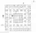
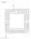
As shown in FIGS. 1 and 2, the semiconductor device of the present embodiment includes a substrate 3 and a semiconductor chip 4. The substrate 3 has a semiconductor-chip mounting portion 1 and external connection terminals 2 on its top surface. The semiconductor chip 4 is mounted over the semiconductor-chip mounting portion 1 of the substrate 3.
Connection terminals 5 are provided on the top surface of the substrate 3, and the semiconductor chip 4 is electrically connected to the connection terminals 5 though connection bumps 6. This state (the state in which the semiconductor chip 4 is electrically connected to the connection terminals 5 through the connection bumps 6) is fixed by an adhesive 7. External connection terminals 8 and connection bumps 9 are provided on the bottom surface of the substrate 3.
The substrate 3 is structured as described above. As shown in FIG. 1, another substrate (substrate 10) is provided over the substrate 3. The structure of the substrate 10 will now be described.
A semiconductor chip 11 and connection terminals 13 are provided on the top surface of the substrate 10. The semiconductor chip 11 and the connection terminals 13 are electrically connected to each other through thin metal wires 12. The semiconductor chip 11, the thin metal wires 12, and the connection terminals 13 are sealed by a sealing resin 14.
This substrate 10 is connected to the substrate 3 by the following method: connection bumps 16 are provided between the external connection terminals 2 on the top surface of the substrate 3 and external connection terminals 15 on the bottom surface of the substrate 10 so that the external connection terminals 2 are electrically and structurally connected to the external connection terminals 15 through the connection bumps 16.
In the present embodiment, the semiconductor device having the substrate 10 over the substrate 3 is structured as described below so that the surface condition of the external connection terminals 2 provided on the top surface of the substrate 3 does not change before the process of bonding the substrate 3 and the substrate 10 together is performed.
As shown in FIG. 2, a plurality of connection terminals 5 are formed as the semiconductor-chip mounting portion 1 in an inner region (central region) of the top surface (front surface) of the substrate 3. A plurality of external connection terminals 2 are formed outside (on the peripheral side of) the semiconductor-chip mounting portion 1 on the top surface of the substrate 3. In other words, the plurality of external connection terminals 2 are formed in the peripheral edge portion of the top surface of the substrate 3. Electroplating wiring patterns 17 are formed so as to extend from the external connection terminals 2 to the outer periphery of the substrate 3. The electroplating wiring patterns 17 are made of a copper film. As shown in FIG. 3, the top surface of each electroplating wiring pattern 17 is covered with a solder resist 18. The solder resist 18 is removed in each region where the external connection terminal 2 is formed, and a terminal portion 2a of the external connection terminal 2 is formed in this region. More specifically, in each region where the solder resist 18 has been removed, an electroless nickel plating layer 19 as a first electroless plating layer, an electroless gold plating layer 20 as a second electroless plating layer, and an electrolytic gold plating layer 21 as an electroplating layer are sequentially formed on the terminal portion 2a of the electroplating wiring pattern (copper layer) 17.
Electric power for forming the electrolytic gold plating layer 21 is supplied through the electroplating wiring patterns 17 extending to the outer periphery of the substrate 3, with the substrate 3 immersed in an electroplating bath.
FIG. 2 shows a state in which the electroplating wiring patterns 17 are separated in the outer periphery of the substrate 3. In the electroplating process, however, a substrate formed by a plurality of substrates 3 (one of them is shown in FIG. 2) integrally connected together in a plane is used, and the electroplating wiring patterns 17 are electrically connected to each other in this substrate.
After the electrolytic gold plating layer 21 is formed by supplying electric power, the substrate is divided into individual substrates 3 as shown in FIG. 2.
FIG. 4 is an enlarged view of one external connection terminal 2 formed as described above. Pd (palladium) plating seeds 22 are present on the electroplating wiring pattern 17. The electroless nickel plating layer 19 is formed by using the Pd plating seeds 22 as plating nuclei. The electroless gold plating layer 20 and the electrolytic gold plating layer 21 are formed over the electroless nickel plating layer 19.
Since the electrolytic gold plating layer 21 is formed by electroplating, the electrolytic plating layer 21 has a dense surface. Accordingly, moisture or the like does not enter through the surface of the electrolytic gold plating layer 21 and, as a matter of course the surface of the electrolytic gold plating layer 21 does not change.
In other words, in the present embodiment, the semiconductor device having the substrate 10 over the substrate 3 as described above includes the electrolytic gold plating layer 21 so that the surface condition of the external connection terminals 2 provided on the top surface of the substrate 3 does not change before the substrate 3 and the substrate 10 are bonded together. Since the surface layer portion of the external connection terminals 2 is made of the electrolytic gold plating layer 21, the connection bumps 16 can be firmly fixed to the electrolytic gold plating layer 21. As a result, bondability between the connection bumps 16 and the external connection terminals 21 can be improved.
In order to form the electrolytic gold plating layer 21, the electroplating wiring patterns 17 made of a copper film are formed so as to extend from the external connection terminals 2 to the outer periphery of the substrate 3.
The electroplating wiring patterns 17 are thus left on the completed substrate 3. The electroplating wiring patterns 17 can therefore suppress peeling off of the external connection terminals 2. More specifically, even if, for example, the substrates 3 and the substrate 10 in FIG. 1 have different thermal expansion coefficients from each other and a force that tries to peel off the external connection terminals 2 through the connection bumps 16 is applied due to the difference in thermal expansion coefficient between the substrates 3 and 10, the electroplating wiring patterns 17 remaining on the substrate 3 will serve as, for example, a root. The electroplating wiring patterns 17 can thus suppress peeling off of the external connection terminals 2.
Note that, in the external connection terminals 8, an electroless nickel plating layer 19 is formed on a terminal portion 8a as shown in FIG. 3, and the connection bumps 9 made of solder balls are provided on the external connection terminals 8. It is herein assumed that, like the external connection terminals 2, the external connection terminals 8 are formed by sequentially forming an electroless nickel plating layer 19, an electroless gold plating layer 20, and an electrolytic gold plating layer 21 on the terminal portion 8a. In this case, if solder balls are provided as the connection bumps 9 on the electrolytic gold plating layer 21, gold plating of the electroless gold plating layer 20 and the electrolytic gold plating layer 21 diffuses into the connection bumps 9. Accordingly, in the external connection terminals 8, the electroless nickel plating layer 19 is formed on the terminal portion 8a as shown in FIG. 3.
As shown in FIG. 5, the external connection terminals 8 are provided on the peripheral edge portion of the bottom surface of the substrate 3. Like the top surface of the substrate 3 (FIG. 2), electroplating wiring patterns 17 made of a copper film may be formed on the bottom surface of the substrate 3 so as to extend from the external connection terminals 8 to the outer periphery of the substrate 3.
The connection terminals 5 may be made of either an electroless plating layer or an electroplating layer. However, the connection terminals 5 are preferably made of an electroless plating layer for the following two reasons: the first reason is to assure the freedom of design of wirings other than the electroplating wirings. More specifically, electroplating wirings need to be formed in order to form the connection terminals 5 from an electroplating layer. However, since the pitch of the connection terminals 5 is narrower than that of the external connection terminals 2 or the like (FIG. 2), forming the electroplating wirings in the mounting portion 1 will almost completely eliminate the freedom of design of wirings other than the electroplating wirings. The second reason is that, since the connection terminals 5 are sealed by the adhesive 7 in a relatively early stage of the manufacturing process of the semiconductor device, moisture can be prevented from entering the connection terminals 5 even if the connection terminals 5 does not have a dense surface layer.
The number of electroless plating layers formed between the terminal portion 2a of the external connection terminals 2 and the electrolytic gold plating layer 21 is not limited to two.
Claims
1-5. (canceled)
6. A semiconductor device, comprising:
a substrate having a top surface, a bottom surface opposite to the top surface, a first external connection terminal, at least two second external connection terminals, and a first wiring pattern; and
a semiconductor chip provided on the top surface;
wherein the top surface comprises a chip area in the middle of the top surface and a peripheral area outside the chip area, and said chip area and said peripheral area do not overlap with one another,
the semiconductor chip is disposed in the chip area,
the first external connection terminal is formed in the peripheral area,
the at least two second external connection terminals are formed in the peripheral area outside the first external connection terminal,
the first wiring pattern extends from the first external connection terminal to an outer periphery of the top surface, and
the first wiring pattern passes through a place between adjacent ones of the at least two second external connection terminals.
7. The semiconductor device according to claim 6, wherein
a second wiring pattern is formed on the top surface, and
the second wiring pattern extends from each of the at least two second external connection terminals to the outer periphery of the top surface.
8. The semiconductor device according to claim 7, wherein multiple ones of the first external connection terminal and the at least two second external connection terminals are disposed in a grid array.
9. The semiconductor device according to claim 8, wherein a third external connection terminal is formed on the bottom surface.
10. The semiconductor device according to claim 9, wherein at least two forth external connection terminals are formed outside the third external connection terminal on the bottom surface.
11. The semiconductor device according to claim 10, wherein
a third wiring pattern extends from the third external connection terminal to an outer periphery of the bottom surface, and
the third wiring pattern passes through a place between adjacent ones of the at least two fourth external connection terminals.
12. The semiconductor device according to claim 11, wherein
a fourth wiring pattern is formed on the bottom surface, and
the forth wiring pattern extends from each of the at least two fourth external connection terminals to the outer periphery of the bottom surface.
13. The semiconductor device according to claim 12, further comprising a plurality of chip connection terminals connected to the semiconductor chip, wherein
the plurality of chip connection terminals are disposed in the chip area.
14. The semiconductor device according to claim 13, wherein the plurality of chip connection terminals are disposed in a grid array.
15. The semiconductor device according to claim 14, wherein
the top surface has a plurality of external connection terminals including the first external connection terminal and the at least two second external connection terminals,
the plurality of external connection terminals are disposed in the peripheral area, and
the plurality of external connection terminals are disposed at substantially equal intervals.
16. The semiconductor device according to claim 15, wherein a size of the first external connection terminal is larger than a size of one of the plurality of chip connection terminals.
17. The semiconductor device according to claim 16, wherein a pitch of the plurality of chip connection terminals is narrower than a pitch of the at least two second external connection terminals.
18. The semiconductor device according to claim 17, wherein the first wiring pattern and the second wiring pattern are covered with a solder resist.
19. The semiconductor device according to claim 18, wherein the first wiring pattern is a Cu wiring pattern.
20. The semiconductor device according to claim 19, wherein the second wiring pattern is a Cu wiring pattern.
21. The semiconductor device according to claim 20, wherein the third wiring pattern is a Cu wiring pattern.
22. The semiconductor device according to claim 21, wherein the fourth wiring pattern is a Cu wiring pattern.
23. The semiconductor device according to claim 22, wherein the first wiring pattern is an electroplating wiring pattern.
24. The semiconductor device according to claim 23, wherein the second wiring pattern is an electroplating wiring pattern.
25. The semiconductor device according to claim 24, wherein the third wiring pattern is an electroplating wiring pattern.
26. The semiconductor device according to claim 25, wherein the fourth wiring pattern is an electroplating wiring pattern.
Images & Drawings included:

Sources:
- United States Patent and Trademark Office - verify current appl. status at the USPTO↗
Similar patent applications:
- » 20110037176
METHOD OF MANUFACTURING A SEMICONDUCTOR DEVICE MODULE, SEMICONDUCTOR DEVICE CONNECTING DEVICE, SEMICONDUCTOR DEVICE MODULE MANUFACTURING DEVICE, SEMICONDUCTOR DEVICE MODULE - » 20230162992
METHOD FOR MANUFACTURING SEMICONDUCTOR DEVICE, METHOD FOR MANUFACTURING DEVICE PROVIDED WITH SEMICONDUCTOR DEVICE, SEMICONDUCTOR DEVICE, AND DEVICE PROVIDED WITH SEMICONDUCTOR DEVICE - » 10889015
Attaching device for mounting and fixing a semiconductor device and a heat sink provided on the semiconductor device on a board, a mount board having the board, the semiconductor device, and the heat sink, and an attaching method of the semiconductor device and the heat sink provided on the semiconductor device on the board - » 20130062745
Semiconductor device, semiconductor device manufacturing method, semiconductor device mounting structure and power semiconductor device - » 20070001197
SEMICONDUCTOR DEVICE, SEMICONDUCTOR DEVICE DESIGN METHOD, SEMICONDUCTOR DEVICE DESIGN METHOD RECORDING MEDIUM, AND SEMICONDUCTOR DEVICE DESIGN SUPPORT SYSTEM - » 10600737
Semiconductor device, semiconductor device design method, semiconductor device design method recording medium, and semiconductor device design support system - » 20130168734
Epitaxial substrate for semiconductor device, semiconductor device, method of manufacturing epitaxial substrate for semiconductor device, and method of manufacturing semiconductor device - » 20110266660
Insulating film for semiconductor device, process and apparatus for producing insulating film for semiconductor device, semiconductor device, and process for producing the semiconductor device - » 20130207111
SEMICONDUCTOR DEVICE, DISPLAY DEVICE INCLUDING SEMICONDUCTOR DEVICE, ELECTRONIC DEVICE INCLUDING SEMICONDUCTOR DEVICE, AND METHOD FOR MANUFACTURING SEMICONDUCTOR DEVICE - » 20170338352
Semiconductor device, display device including semiconductor device, electronic device including semiconductor device, and method for manufacturing semiconductor device
Recent applications in this class:
- » 20250293143 2025-09-18
ORGANIC INTERPOSER INCLUDING INTRA-DIE STRUCTURAL REINFORCEMENT STRUCTURES AND METHODS OF FORMING THE SAME - » 20250293142 2025-09-18
SEMICONDUCTOR MODULE - » 20250293141 2025-09-18
PACKAGE SUBSTRATE AND SEMICONDUCTOR PACKAGE INCLUDING THE SAME - » 20250293140 2025-09-18
SEMICONDUCTOR DEVICE - » 20250293139 2025-09-18
SEMICONDUCTOR PACKAGE - » 20250293138 2025-09-18
PACKAGE STRUCTURE AND MANUFACTURING METHOD THEREOF - » 20250293137 2025-09-18
3D DIE STACK REDISTRIBUTION LAYER FOR TOPSIDE POWER DELIVERY TO BACKSIDE DIE METALLIZATION IN MULTICHIP COMPOSITE DEVICES - » 20250293136 2025-09-18
BURIED BUMP STRUCTURE - » 20250293135 2025-09-18
VERTICAL CIRCUIT DIE WITH LATERAL SIDE METAL - » 20250285959 2025-09-11
METHOD OF FABRICATING PACKAGE STRUCTURE
Recent applications for this Assignee:
- » 20250038213 2025-01-30
SLURRY FOR NON-AQUEOUS ELECTROLYTE SECONDARY CELL, METHOD FOR MANUFACTURING SLURRY FOR NON-AQUEOUS ELECTROLYTE SECONDARY CELL, ELECTRODE FOR NON-AQUEOUS ELECTROLYTE SECONDARY CELL, AND NON-AQUEOUS ELECTROLYTE SECONDARY CELL - » 20230388751 2023-11-30
Information providing method and information providing apparatus - » 20230187624 2023-06-15
Positive electrode active material for lithium ion secondary battery and lithium ion secondary battery - » 20220368162 2022-11-17
POWER TRANSMISSION COIL, POWER TRANSMISSION DEVICE, AND UNDERWATER POWER SUPPLY SYSTEMS - » 20220345978 2022-10-27
NETWORK CONTROL DEVICE, NETWORK CONTROL SYSTEM, AND NETWORK CONTROL METHOD - » 20220345847 2022-10-27
Information collecting method, communication control apparatus, and information collector apparatus - » 20220317284 2022-10-06
SURVEILLANCE SYSTEM, AND SURVEILLANCE METHOD - » 20220299596 2022-09-22
MONITORING DEVICE AND MONITORING METHOD - » 20220278402 2022-09-01
RECTANGULAR SECONDARY BATTERY - » 20220205908 2022-06-30
Cellulose composite determination method and apparatus for composite resin