Bonding material, method, and structure
US20120107631A1
2012-05-03
13/283,490
2011-10-27
✅ Patent granted
US 8,808,494 B2
2014-08-19
-
-
Vera Katz
2032-08-27
Abstract:
Disclosed is a bonding structure, including a heat dissipation substrate, a eutectic layer on the heat dissipation substrate, and a copper layer on the eutectic layer. The thermal dissipation substrate includes aluminum oxide, aluminum nitride, or zirconium oxide. The eutectic layer includes aluminum oxide, aluminum nitride, or zirconium oxide doped with zinc, tin, indium, or combinations thereof.
Assignee:
- INDUSTRIAL TECHNOLOGY RESEARCH INSTITUTE 7,890 🇹🇼 HSINCHU, Taiwan
Applicant:
Interested in similar patents?
Get notified when new applications in this technology area are published.
Classification:
C04B37/028 » CPC main
Joining burned ceramic articles with other burned ceramic articles or other articles by heating with metallic articles by means of an interlayer consisting of an organic adhesive, e.g. phenol resin or pitch
Y10T428/12056 » CPC further
Stock material or miscellaneous articles; All metal or with adjacent metals having metal particles; Composite; i.e., plural, adjacent, spatially distinct metal components [e.g., layers, etc.]; Nonmetal component Entirely inorganic
H01L2924/0002 » CPC further
Indexing scheme for arrangements or methods for connecting or disconnecting semiconductor or solid-state bodies as covered by; Technical content checked by a classifier Not covered by any one of groups , and
H01L2924/00 » CPC further
Indexing scheme for arrangements or methods for connecting or disconnecting semiconductor or solid-state bodies as covered by
C04B2237/60 » CPC further
Aspects relating to ceramic laminates or to joining of ceramic articles with other articles by heating; Processing aspects relating to ceramic laminates or to the joining of ceramic articles with other articles by heating Forming at the joining interface or in the joining layer specific reaction phases or zones, e.g. diffusion of reactive species from the interlayer to the substrate or from a substrate to the joining interface, carbide forming at the joining interface
C04B2235/5445 » CPC further
Aspects relating to ceramic starting mixtures or sintered ceramic products; Composition of constituents of the starting material or of secondary phases of the final product; Constituents or additives of the starting mixture chosen for their shape or used because of their shape or their physical appearance; Particle size related information expressed by the size of the particles or aggregates thereof submicron sized, i.e. from 0,1 to 1 micron
C04B2235/5454 » CPC further
Aspects relating to ceramic starting mixtures or sintered ceramic products; Composition of constituents of the starting material or of secondary phases of the final product; Constituents or additives of the starting mixture chosen for their shape or used because of their shape or their physical appearance; Particle size related information expressed by the size of the particles or aggregates thereof nanometer sized, i.e. below 100 nm
C04B2237/407 » CPC further
Aspects relating to ceramic laminates or to joining of ceramic articles with other articles by heating; Composition of layers of ceramic laminates or of ceramic or metallic articles to be joined by heating, e.g. Si substrates; Metallic Copper
C04B2237/72 » CPC further
Aspects relating to ceramic laminates or to joining of ceramic articles with other articles by heating; Processing aspects relating to ceramic laminates or to the joining of ceramic articles with other articles by heating Forming laminates or joined articles comprising at least two interlayers directly next to each other
C04B37/025 » CPC further
Joining burned ceramic articles with other burned ceramic articles or other articles by heating with metallic articles characterised by the interlayer used consisting of glass or ceramic material
H01L33/641 » CPC further
Semiconductor devices with at least one potential-jump barrier or surface barrier specially adapted for light emission; Processes or apparatus specially adapted for the manufacture or treatment thereof or of parts thereof; Details thereof characterised by the semiconductor body packages; Heat extraction or cooling elements characterized by the materials
C04B2237/708 » CPC further
Aspects relating to ceramic laminates or to joining of ceramic articles with other articles by heating; Processing aspects relating to ceramic laminates or to the joining of ceramic articles with other articles by heating; Forming laminates or joined articles comprising layers of a specific, unusual thickness of one or more of the interlayers
C04B2237/348 » CPC further
Aspects relating to ceramic laminates or to joining of ceramic articles with other articles by heating; Composition of layers of ceramic laminates or of ceramic or metallic articles to be joined by heating, e.g. Si substrates; Ceramic; Oxidic; Refractory metal oxides Zirconia, hafnia, zirconates or hafnates
C04B2237/06 » CPC further
Aspects relating to ceramic laminates or to joining of ceramic articles with other articles by heating; Aspects relating to interlayers, e.g. used to join ceramic articles with other articles by heating; Ceramic interlayers Oxidic interlayers
C04B2235/3281 » CPC further
Aspects relating to ceramic starting mixtures or sintered ceramic products; Composition of constituents of the starting material or of secondary phases of the final product; Constituents and secondary phases not being of a fibrous nature; Metal oxides, mixed metal oxides, or oxide-forming salts thereof, e.g. carbonates, nitrates, (oxy)hydroxides, chlorides Copper oxides, cuprates or oxide-forming salts thereof, e.g. CuO or CuO
C04B2237/366 » CPC further
Aspects relating to ceramic laminates or to joining of ceramic articles with other articles by heating; Composition of layers of ceramic laminates or of ceramic or metallic articles to be joined by heating, e.g. Si substrates; Ceramic; Non-oxidic Aluminium nitride
C04B2237/068 » CPC further
Aspects relating to ceramic laminates or to joining of ceramic articles with other articles by heating; Aspects relating to interlayers, e.g. used to join ceramic articles with other articles by heating; Ceramic interlayers; Oxidic interlayers based on refractory oxides, e.g. zirconia
C04B2237/592 » CPC further
Aspects relating to ceramic laminates or to joining of ceramic articles with other articles by heating; Processing aspects relating to ceramic laminates or to the joining of ceramic articles with other articles by heating; Aspects relating to the structure of the interlayer whereby the interlayer is not continuous, e.g. not the whole surface of the smallest substrate is covered by the interlayer
C04B2237/343 » CPC further
Aspects relating to ceramic laminates or to joining of ceramic articles with other articles by heating; Composition of layers of ceramic laminates or of ceramic or metallic articles to be joined by heating, e.g. Si substrates; Ceramic; Oxidic Alumina or aluminates
B32B15/04 IPC
Layered products comprising a layer of metal comprising metal as the main or only constituent of a layer, next to another layer of a
B32B15/20 IPC
Layered products comprising a layer of metal comprising aluminium or copper
B32B37/06 IPC
Methods or apparatus for laminating, e.g. by curing or by ultrasonic bonding characterised by the heating method
B32B37/14 IPC
Methods or apparatus for laminating, e.g. by curing or by ultrasonic bonding characterised by the properties of the layers
B32B18/00 IPC
Layered products essentially comprising ceramics, e.g. refractory products
B32B37/12 IPC
Methods or apparatus for laminating, e.g. by curing or by ultrasonic bonding characterised by using adhesives
C08L1/00 IPC
Compositions of cellulose, modified cellulose or cellulose derivatives
C08L1/00 IPC
Compositions of polysaccharides or of their derivatives
C08K3/22 IPC
Use of inorganic substances as compounding ingredients; Oxygen-containing compounds, e.g. metal carbonyls; Oxides; Hydroxides of metals
B82Y30/00 » CPC further
Nanotechnology for materials or surface science, e.g. nanocomposites
C04B35/6365 » CPC further
Shaped ceramic products characterised by their composition ; Ceramics compositions ; Processing powders of inorganic compounds preparatory to the manufacturing of ceramic products; Forming processes; Processing powders of inorganic compounds preparatory to the manufacturing of ceramic products; Preparing or treating the powders individually or as batches ; preparing or treating macroscopic reinforcing agents for ceramic products, e.g. fibres; mechanical aspects section using additives specially adapted for forming the products, e.g.. binder binders; Organic additives; Polysaccharides or derivatives thereof Cellulose or derivatives thereof
C04B2237/08 » CPC further
Aspects relating to ceramic laminates or to joining of ceramic articles with other articles by heating; Aspects relating to interlayers, e.g. used to join ceramic articles with other articles by heating; Ceramic interlayers Non-oxidic interlayers
C04B35/636 IPC
Shaped ceramic products characterised by their composition ; Ceramics compositions ; Processing powders of inorganic compounds preparatory to the manufacturing of ceramic products; Forming processes; Processing powders of inorganic compounds preparatory to the manufacturing of ceramic products; Preparing or treating the powders individually or as batches ; preparing or treating macroscopic reinforcing agents for ceramic products, e.g. fibres; mechanical aspects section using additives specially adapted for forming the products, e.g.. binder binders; Organic additives Polysaccharides or derivatives thereof
C04B37/02 IPC
Joining burned ceramic articles with other burned ceramic articles or other articles by heating with metallic articles
C04B35/634 IPC
Shaped ceramic products characterised by their composition ; Ceramics compositions ; Processing powders of inorganic compounds preparatory to the manufacturing of ceramic products; Forming processes; Processing powders of inorganic compounds preparatory to the manufacturing of ceramic products; Preparing or treating the powders individually or as batches ; preparing or treating macroscopic reinforcing agents for ceramic products, e.g. fibres; mechanical aspects section using additives specially adapted for forming the products, e.g.. binder binders; Organic additives Polymers
H01L33/64 IPC
Semiconductor devices with at least one potential-jump barrier or surface barrier specially adapted for light emission; Processes or apparatus specially adapted for the manufacture or treatment thereof or of parts thereof; Details thereof characterised by the semiconductor body packages Heat extraction or cooling elements
C04B2235/9607 » CPC further
Aspects relating to ceramic starting mixtures or sintered ceramic products; Aspects relating to sintered or melt-casted ceramic products; Properties of ceramic products, e.g. mechanical properties such as strength, toughness, wear resistance Thermal properties, e.g. thermal expansion coefficient
C04B2237/064 » CPC further
Aspects relating to ceramic laminates or to joining of ceramic articles with other articles by heating; Aspects relating to interlayers, e.g. used to join ceramic articles with other articles by heating; Ceramic interlayers; Oxidic interlayers based on alumina or aluminates
Description
CROSS REFERENCE TO RELATED APPLICATIONS
This application claims priority of Taiwan Patent Application No. 099137590, filed on Nov. 2, 2010, the entirety of which is incorporated by reference herein.
BACKGROUND
1. Field
The disclosure relates to a bonding structure, and in particular relates to a bonding material and a bonding method for bonding a copper sheet to a heat dissipation substrate.
2. Description of the Related Art
Improving upon heat dissipation has reached a bottleneck for modulating a high heat generating device. Conventional FR4 substrates or aluminum-based metal substrates cannot conduct heat from a device to a heat dissipation device due to their low thermal conductivities. The described problem can be overcome by combining a copper sheet with an electrically insulative ceramic substrate to conduct the heat from a device to the heat dissipation device. The composite plate is the so-called direct bonded copper (DBC).
Although DBC may solve the heat dissipation problem, it is often processed at a temperature of over 1000° C. For forming a eutectic layer between the copper sheet and the ceramic substrate, the copper sheet should be firstly oxidized to form a copper oxide layer to bond with the ceramic substrate. Controlling uniformity and thickness of the copper oxide layer is difficult, thus, often, non-uniform heat dissipation results. If the copper layer needs to be patterned, an additional patterning process such as lithography and etching will be performed.
Accordingly, a novel method for bonding the copper sheet and the thermal dissipation substrate is called-for.
BRIEF SUMMARY
One embodiment of the disclosure provides a bonding material, comprising: an organic polymer; and an inorganic powder averagely dispersed in the organic polymer, wherein the organic polymer and the inorganic powder have a weight ratio of 50:50 to 10:90, and wherein the inorganic powder comprises copper oxide averagely mixed with a dopant, wherein the copper oxide and the dopant have a molar ratio of 99.5:0.5 to 99.9:0.1, and the dopant is zinc, tin, indium, or combinations thereof.
One embodiment of the disclosure provides a bonding method, comprising: bonding a heat dissipation substrate and a copper layer by the described bonding material; and heating the bonding material, such that the inorganic powder of the bonding material, a part of the heat dissipation substrate, and a part of the copper layer form a eutectic layer.
One embodiment of the disclosure provides a bonding structure, comprising: a heat dissipation substrate; a eutectic layer on the heat dissipation substrate; and a copper layer on the eutectic layer, wherein the heat dissipation substrate comprises aluminum oxide, aluminum nitride, or zirconium oxide, and the eutectic layer comprises copper aluminum oxide, copper aluminum oxynitride, or copper zirconium oxide doped with zinc, tin, indium, or combinations thereof.
A detailed description is given in the following embodiments with reference to the accompanying drawings.
BRIEF DESCRIPTION OF THE DRAWINGS
The disclosure can be more fully understood by reading the subsequent detailed description and examples with references made to the accompanying drawings, wherein:
FIGS. 1-3 show a process of forming a bonding structure in one embodiment of the disclosure.
DETAILED DESCRIPTION
The following description is of the best-contemplated mode of carrying out the disclosure. This description is made for the purpose of illustrating the general principles of the disclosure and should not be taken in a limiting sense. The scope of the disclosure is best determined by reference to the appended claims.
One embodiment provides a bonding material including an organic polymer and an inorganic powder. The organic polymer can be PVB, PVA, methyl cellulose, other suitable organic polymers, or combinations thereof. In one embodiment, the organic polymer has a viscosity of 300 cps to 10000 cps. An organic polymer having an overly high viscosity may form an overly thick coating and cannot be averagely coated onto a heat dissipation substrate. An organic polymer having an overly low viscosity cannot be adhered onto a heat dissipation substrate. In one embodiment, the organic polymer has a weight average molecular weight of 8000 to 20000. An organic polymer having an overly high weight average molecular weight easily leaves carbon after heating. An organic polymer having an overly low weight average molecular weight will form a film of low strength, wherein the film easily peels after being coated onto a heat dissipation substrate. The inorganic powder includes copper oxide averagely mixed with a dopant. The dopant is zinc, tin, indium, or combinations thereof. The copper oxide and the dopant have a molar ratio of 99.5:0.5 to 99.9:0.1. A dopant having an overly high doping ratio may increase material costs without obviously decreasing bonding temperatures, and may further make bonding interference brittle. A dopant having an overly low doping ratio cannot efficiently decrease bonding temperatures. The copper oxide and the dopant are averagely mixed to form the inorganic powder having a diameter distribution of 20 nm to 300 nm. The diameter distribution of the inorganic powder helps the inorganic powder to be averagely dispersed in the organic polymer. In addition, a dispersant may further help the inorganic powder to be averagely suspended rather than precipitated in the colloid. An inorganic powder having an overly large diameter may increase the temperature when forming a eutectic layer. An inorganic powder having an overly small diameter is difficult to be dispersed in the organic polymer. Thereafter, the inorganic powder is averagely dispersed in the organic polymer to form a bonding material by ball grinding, stirring, or high speed centrifuge. The organic polymer and the inorganic powder have a weight ratio of 50:50 to 10:90. An inorganic powder having an overly high ratio will make the bonding material have too high a viscosity for coating. An inorganic powder having an overly low ratio will make the bonding material difficult to be formed into a film having a sufficient thickness. The bonding material can be gel or liquid, which depends on the type of process used.
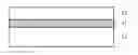
As shown in FIG. 1, the bonding material 11 is coated on a heat dissipation substrate 13 by spin coating, inkjet printing, slit die coating, dip coating, or combinations thereof. The heat dissipation substrate 13 can be a ceramic material such as aluminum oxide, aluminum nitride, zirconium oxide, or other materials which may combine with copper oxide to form a eutectic layer.
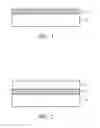
As shown in FIG. 2, a copper layer 15 is then formed on the bonding material 11. In one embodiment, the copper layer 15 has a thickness of 100 μm to 500 μm. The copper layer 15 is used to support and bond to a heat generating device such as an LED, IC, or the likes. The heat generating device can be bonded to the copper layer by flip-chip, wire bonding, other known bonding methods, or future developed bonding methods. An overly thin copper layer easily deforms. An overly thick copper layer has low adhering strength and non-average interference with the bonding material.
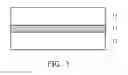
As shown in FIG. 3, the described structure is heated, such that the inorganic powder of the bonding material 11, the surface of the heat dissipation substrate 13, and the surface of the copper layer 15 form a eutectic layer 17. In one embodiment, the heating step of forming the eutectic layer 17 is performed at a temperature of 950° C. to 1000° C. In another embodiment, the heating step of forming the eutectic layer 17 is performed at a temperature of 950° C. to 980° C. Compared to conventional art, the heating step of forming the eutectic layer 17 in the disclosure is performed at a lower temperature, thereby efficiently saving energy and decreasing safety risk. As such, description of a bonding structure of the disclosure is completed. In some embodiments, the heating step not only forms the eutectic layer 17, but also removes the organic polymer in the bonding material 11. In other embodiments, additional steps can be introduced before the heating step to remove the organic polymer in the bonding material 11. The additional steps include low temperature baking to form a film (60° C. to 120° C.), middle temperature degreasing (200° C. to 500° C.), and high temperature fusion (600° C. to 1100° C.).
In one embodiment, the heat dissipation substrate 13 is aluminum oxide (Al2O3), and the eutectic layer 17 is copper aluminum oxide (CuAl2O4) doped with zinc, tin, indium, or combinations thereof. In another embodiment, the heat dissipation substrate 13 is aluminum nitride (AlN), and the eutectic layer 17 is copper aluminum oxynitride (CuAlNO) doped with zinc, tin, indium, or combinations thereof. In a further embodiment, the heat dissipation substrate 13 is zirconium oxide (ZrO2), and the eutectic layer 17 is copper zirconium copper oxide (CuZrO3) doped with zinc, tin, indium, or combinations thereof.
The described eutectic layer 17 can be analyzed by a chip test to determine its thickness of 1 μm to 20 μm. The thickness of the eutectic layer 17 is controlled by the thickness of the bonding material 11. An overly thin eutectic layer or a bonding material has low adhering strength with the copper layer and/or the heat dissipation substrate. An overly thick eutectic layer or a bonding material has low heat dissipation property.
In one embodiment, a heat generating device on the copper layer may endure a high temperature. As such, one side of the copper layer 15 can be firstly bonded to the heat generating device, and the other side of the copper layer can be then disposed onto the bonding material 11. In another embodiment, the described bonding structure is firstly formed, and the heat generating device is then bonded onto the copper layer 15. It should be understood that the copper layer 15 and the bonding material 11 belong to different processes, and the copper layer 15 adhered onto the bonding material layer 11 can be a continuously layered structure or a discontinuous pattern. Compared to the conventional art, a discontinuous pattern of the copper layer 15 can be directly adhered onto the bonding material 11 without the risk of damaging the eutectic layer 17 due to an etching process for patterning the copper layer 15.
In one embodiment, heat generated by a device on the copper layer 15 can be directly dissipated to surrounding areas through the copper layer 15, the eutectic layer 17, and the heat dissipation substrate 13. In some embodiments, other heat dissipation devices such as a fan, thermal pipe, or other heat dissipation devices, or combinations thereof can be set under the heat dissipation substrate 13 to further accelerate the heat dissipation effect.
EXAMPLE
Comparative Example 1
40 g of copper oxide nanoparticles formed by a chemical method were dispersed in 60 g of organic polymer slurry (BP series binder, commercially available from Exojet Technology Corporation) to form a bonding material. The chemical method firstly dispersed metal ions in a polymer solution, wherein the concentrations of the metal ions were exactly controlled to correspond to metal ratios of a desired composition. The metal ions were adsorbed by a chelate to form a metal complex, which was then degraded by heating to from a nano oxide. The copper oxide nanoparticles were dispersed in the organic slurry by a three-roller mill (EXAKT-35, commercially available from KOENEN) at an operation speed of 2 l/h to 3 l/h for 30 minutes to 120 minutes. The bonding material was then spin coated on an aluminum oxide substrate (96% aluminum oxide with a thermal conductivity of 20 W/mK, commercially available form LEATEC Fine Ceramics Co., Ltd), and a copper foil having a thickness of 300 μm was then adhered to the bonding material. The described structure was heated, such that the bonding material, a part of the copper foil contacting the bonding material, and a part of the aluminum oxide substrate contacting the bonding material formed a eutectic layer having a thickness of 0.5 μm to 3 μm. The final bonding structure had a thermal conductivity of 40 W/mK, and the heating step of forming the eutectic layer was performed at a temperature of about 1020° C.
Example 1-1
Example 1-1 was substantially similar to Comparative Example 1, and the difference therebetween was that the copper oxide nanoparticles in Example 1-1 were doped with 0.1 mole % zinc. The final bonding structure in Example 1-1 had a thermal conductivity of 38 W/mK (higher than that of the aluminum oxide substrate), and the heating step of forming the eutectic layer having a thickness of 0.5 μm to 3 μm was performed at a temperature of about 980° C.
Example 1-2
Example 1-2 was substantially similar to Comparative Example 1, and the difference therebetween was that the copper oxide nanoparticles in Example 1-2 were doped with 0.3 mole % zinc. The final bonding structure in Example 1-2 had a thermal conductivity of 30 W/mK (higher than that of the aluminum oxide substrate), and the heating step of forming the eutectic layer having a thickness of 0.5 μm to 3 μm was performed at a temperature of about 960° C.
Example 1-3
Example 1-3 was substantially similar to Comparative Example 1, and the difference therebetween was that the copper oxide nanoparticles in Example 1-3 were doped with 0.5 mole % zinc. The final bonding structure in Example 1-3 had a thermal conductivity of 30 W/mK (higher than that of the aluminum oxide substrate), and the heating step of forming the eutectic layer having a thickness of 0.5 μm to 3 μm was performed at a temperature of about 960° C. According to a comparison between Comparative Example 1 and Examples 1-1, 1-2, and 1-3, the copper oxide nanoparticles doped with the appropriate amount of zinc efficiently decreased the formation temperature of the eutectic layer without sacrificing the thermal conductivity of the bonding structure.
Example 2-1
Example 2-1 was substantially similar to Comparative Example 1, and the difference therebetween was that the copper oxide nanoparticles in Example 2-1 were doped with 0.1 mole % tin. The final bonding structure in Example 2-1 had a thermal conductivity of 35 W/mK (higher than that of the aluminum oxide substrate), and the heating step of forming the eutectic layer having a thickness of 0.5 μm to 3 μm was performed at a temperature of about 970° C.
Example 2-2
Example 2-2 was substantially similar to Comparative Example 1, and the difference therebetween was that the copper oxide nanoparticles in Example 2-2 were doped with 0.3 mole % tin. The final bonding structure in Example 2-2 had a thermal conductivity of 35 W/mK (higher than that of the aluminum oxide substrate), and the heating step of forming the eutectic layer having a thickness of 0.5 μm to 3 μm was performed at a temperature of about 950° C.
Example 2-3
Example 2-3 was substantially similar to Comparative Example 1, and the difference therebetween was that the copper oxide nanoparticles in Example 2-3 were doped with 0.5 mole % tin. The final bonding structure in Example 2-3 had a thermal conductivity of 30 W/mK (higher than that of the aluminum oxide substrate), and the heating step of forming the eutectic layer having a thickness of 0.5 μm to 3 μm was performed at a temperature of about 950° C. According to a comparison between Comparative Example 1 and Examples 2-1, 2-2, and 2-3, the copper oxide nanoparticles doped with the appropriate amount of tin efficiently decreased the formation temperature of the eutectic layer without sacrificing the thermal conductivity of the bonding structure.
Example 3-1
Example 3-1 was substantially similar to Comparative Example 1, and the difference therebetween was that the copper oxide nanoparticles in Example 3-1 were doped with 0.1 mole % indium. The final bonding structure in Example 3-1 had a thermal conductivity of 34 W/mK (higher than that of the aluminum oxide substrate), and the heating step of forming the eutectic layer having a thickness of 0.5 μm to 3 μm was performed at a temperature of about 980° C.
Example 3-2
Example 3-2 was substantially similar to Comparative Example 1, and the difference therebetween was that the copper oxide nanoparticles in Example 3-2 were doped with 0.1 mole % indium. The final bonding structure in Example 3-2 had a thermal conductivity of 33 W/mK (higher than that of the aluminum oxide substrate), and the heating step of forming the eutectic layer having a thickness of 0.5 μm to 3 μm was performed at a temperature of about 980° C.
Example 3-3
Example 3-3 was substantially similar to Comparative Example 1, and the difference therebetween was that the copper oxide nanoparticles in Example 3-3 were doped with 0.5 mole % indium. The final bonding structure in Example 3-3 had a thermal conductivity of 33 W/mK (higher than that of the aluminum oxide substrate), and the heating step of forming the eutectic layer having a thickness of 0.5 μm to 3 μm was performed at a temperature of about 960° C. According to a comparison between Comparative Example 1 and Examples 3-1, 3-2, and 3-3, the copper oxide nanoparticles doped with the appropriate amount of indium efficiently decreased formation temperature of the eutectic layer without sacrificing the thermal conductivity of the bonding structure.
While the disclosure has been described by way of example and in terms of the preferred embodiments, it is to be understood that the disclosure is not limited to the disclosed embodiments. To the contrary, it is intended to cover various modifications and similar arrangements (as would be apparent to those skilled in the art). Therefore, the scope of the appended claims should be accorded the broadest interpretation so as to encompass all such modifications and similar arrangements.
Claims
What is claimed is:1. A bonding material, comprising:
an organic polymer; and
an inorganic powder dispersed in the organic polymer,
wherein the organic polymer and the inorganic powder have a weight ratio of 50:50 to 10:90, and
wherein the inorganic powder comprises copper oxide averagely mixed with a dopant, wherein the copper oxide and the dopant have a molar ratio of 99.5:0.5 to 99.9:0.1, and the dopant is zinc, tin, indium, or combinations thereof.
2. The bonding material as claimed in claim 1, wherein the organic polymer comprises PVB, PVA, methyl cellulose, or combinations thereof.
3. The bonding material as claimed in claim 1, wherein the inorganic powder has a diameter distribution of 20 nm to 300 nm.
4. A bonding method, comprising:
bonding a heat dissipation substrate and a copper layer by the bonding material as claimed in claim 1; and
heating the bonding material, such that the inorganic powder of the bonding material, a part of the heat dissipation substrate, and a part of the copper layer form a eutectic layer.
5. The bonding method as claimed in claim 4, wherein the heat dissipation substrate comprises aluminum oxide, aluminum nitride, or zirconium oxide, and the eutectic layer comprises copper aluminum oxide, copper aluminum oxynitride, or copper zirconium oxide doped with zinc, tin, indium, or combinations thereof.
6. The bonding method as claimed in claim 4, wherein the step of heating the bonding material to form the eutectic layer is performed at a temperature of 950° C. to 1000° C.
7. The bonding method as claimed in claim 4, wherein the step of heating the bonding material to form the eutectic layer is performed under an atmosphere of nitrogen.
8. The bonding method as claimed in claim 4, wherein the step of bonding a heat dissipation substrate and a copper layer by the bonding material comprises printing or spin coating.
9. A bonding structure, comprising:
a heat dissipation substrate;
a eutectic layer on the heat dissipation substrate; and
a copper layer on the eutectic layer,
wherein the heat dissipation substrate comprises aluminum oxide, aluminum nitride, or zirconium oxide, and the eutectic layer comprises copper aluminum oxide, copper aluminum oxynitride, or copper zirconium oxide doped with zinc, tin, indium, or combinations thereof.
10. The bonding structure as claimed in claim 9, wherein the eutectic layer and/or the copper layer comprises a continuously layered structure or a discontinuous pattern.
11. The bonding structure as claimed in claim 9, wherein the eutectic layer has a thickness of 1 μm to 20 μm.
12. The bonding structure as claimed in claim 9, wherein the copper layer has a thickness of 100 μm to 500 μm.
Images & Drawings included:
Sources:
- United States Patent and Trademark Office - verify current appl. status at the USPTO↗
Similar patent applications:
- » 20170232562
BONDING STRUCTURE, BONDING MATERIAL AND BONDING METHOD - » 20180297152
Bonding material, and bonding method and bonded structure each using same - » 20160280937
Circumference coating material, bonding material, honeycomb structure, and method of producing honeycomb structure - » 20220371120
Dissimilar material solid phase bonding method, dissimilar material solid phase bonded structure, and dissimilar material solid phase bonding device - » 20200090951
Transient liquid phase material bonding and sealing structures and methods of forming same - » 20190047093
Bonding material, method for producing bonding material, and method for producing bonding structure - » 20170086320
Transient liquid phase material bonding and sealing structures and methods of forming same - » 20200070429
BOND CONSTRUCTION AND BONDING METHOD OF FRP MATERIAL TO STRUCTURE - » 20170036432
Manufacturing method of honeycomb structure, and bonding material - » 20250079185
METHOD OF BONDING SEMICONDUCTOR MATERIALS AND STRUCTURE FORMED BY THE SAME
Recent applications in this class:
- » 20230365471 2023-11-16
COMPOSITE SHEET AND METHOD FOR PRODUCING SAME, AND MULTILAYER BODY AND METHOD FOR PRODUCING SAME, AND POWER DEVICE - » 20230357090 2023-11-09
COMPOSITE SHEET, LAMINATE, AND EVALUATION METHOD FOR ESTIMATING ADHESIVENESS OF COMPOSITE SHEET - » 20230357089 2023-11-09
COMPOSITE SHEET AND MANUFACTURING METHOD THEREOF, AND LAMINATE AND MANUFACTURING METHOD THEREOF - » 20210292247 2021-09-23
Ceramic structural body - » 20190210931 2019-07-11
Polycrystalline diamond compact - » 20110274888 2011-11-10
Composite Material, Method for Producing a Composite Material and Adhesive or Binding Material - » 20060257636 2006-11-16
Thermally stable and liquid-tight joint between a first ceramic, metal, or plastic component and a second ceramic, metal or plastic component, and the use of one such joint
Recent applications for this Assignee:
- » 20250289330 2025-09-18
MOBILE VEHICLE CHARGING PROTECTION DEVICE FOR ELECTRICAL SAFETY IN LIVESTOCK HOUSES - » 20250287224 2025-09-11
COMMUNICATION DEVICE AND COMMUNICATION METHOD - » 20250286593 2025-09-11
COMMUNICATION DEVICE AND METHOD OF BEAM MANAGEMENT - » 20250284336 2025-09-11
SYSTEM AND METHOD FOR ADJUSTING IMAGE BASED ON PHYSIOLOGICAL INFORMATION AND POSTURE - » 20250281908 2025-09-11
ELECTROCATALYST COMPOSITION AND PREPARATION METHOD THEREOF - » 20250273403 2025-08-28
CAPACITOR AND ELECTRONIC DEVICE - » 20250271759 2025-08-28
POLYMER, POSITIVE PHOTORESIST COMPOSITION, AND METHOD FOR FORMING PATTERNED PHOTORESIST LAYER - » 20250265803 2025-08-21
MULTI-SENSOR COORDINATION METHOD, PROCESSING DEVICE, AND INFORMATION DISPLAY SYSTEM - » 20250263659 2025-08-21
METHOD AND KIT FOR PREPARING AN IMMUNE CELL DIFFERENTIATED FROM A STEM CELL - » 20250252547 2025-08-07
CORROSION POSITIONING SYSTEM, CORROSION INSPECTION VEHICLE AND CORROSION POSITIONING METHOD USING THE SAME