Light emitting diode package and method for manufacturing the same
US20120126264A1
2012-05-24
13/209,448
2011-08-15
✅ Patent granted
US 8,507,934 B2
2013-08-13
-
-
Victor A Mandala
Altis Law Group, Inc.
2032-01-03
Abstract:
An exemplary light emitting diode (LED) package includes a substrate having a first electrical portion and a second electrical portion formed thereon, two antioxidation layers formed on and electrically connected to the first electrical portion and the second electrical portion, respectively, and an LED chip disposed on the substrate and electrically connected to the two antioxidation layers.
Inventors:
- CHAO-HSIUNG CHANG 46 🇹🇼 Hukou, Taiwan
- PI-CHIANG HU 7 🇹🇼 Hsinchu, Taiwan
- PI-CHIANG HU 7 🇹🇼 Hukou, Taiwan
- CHIEH-LING CHANG 9 🇹🇼 Hsinchu, Taiwan
- Chao-Hsiung Chang 49 🇹🇼 Hsinchu, Taiwan
- CHIEH-LING CHANG 5 🇹🇼 Hukou, Taiwan
Assignee:
- ADVANCED OPTOELECTRONIC TECHNOLOGY, INC. 432 🇹🇼 Hsinchu Hsien, Taiwan
- Advanced Optoelectronics Technology, Inc. 19 🇹🇼 Hsinchu Hsien, Taiwan
Applicant:
Interested in similar patents?
Get notified when new applications in this technology area are published.
Classification:
H01L33/486 » CPC main
Semiconductor devices with at least one potential-jump barrier or surface barrier specially adapted for light emission; Processes or apparatus specially adapted for the manufacture or treatment thereof or of parts thereof; Details thereof characterised by the semiconductor body packages; Containers adapted for surface mounting
H01L24/97 » CPC further
Arrangements for connecting or disconnecting semiconductor or solid-state bodies; Methods or apparatus related thereto; Batch processes at chip-level, i.e. with connecting carried out on a plurality of singulated devices, i.e. on diced chips the devices being connected to a common substrate, e.g. interposer, said common substrate being separable into individual assemblies after connecting
H01L33/62 » CPC further
Semiconductor devices with at least one potential-jump barrier or surface barrier specially adapted for light emission; Processes or apparatus specially adapted for the manufacture or treatment thereof or of parts thereof; Details thereof characterised by the semiconductor body packages Arrangements for conducting electric current to or from the semiconductor body, e.g. lead-frames, wire-bonds or solder balls
H01L2924/12041 » CPC further
Indexing scheme for arrangements or methods for connecting or disconnecting semiconductor or solid-state bodies as covered by; Details of semiconductor or other solid state devices to be connected; Device type; Passive devices, e.g. 2 terminal devices; Optical Diode LED
H01L2924/00012 » CPC further
Indexing scheme for arrangements or methods for connecting or disconnecting semiconductor or solid-state bodies as covered by; Technical content checked by a classifier Relevant to the scope of the group, the symbol of which is combined with the symbol of this group
H01L2924/00014 » CPC further
Indexing scheme for arrangements or methods for connecting or disconnecting semiconductor or solid-state bodies as covered by; Technical content checked by a classifier the subject-matter covered by the group, the symbol of which is combined with the symbol of this group, being disclosed without further technical details
H01L2224/97 » CPC further
Indexing scheme for arrangements for connecting or disconnecting semiconductor or solid-state bodies and methods related thereto as covered by; Batch processes at chip-level, i.e. with connecting carried out on a plurality of singulated devices, i.e. on diced chips the devices being connected to a common substrate, e.g. interposer, said common substrate being separable into individual assemblies after connecting
H01L2224/85 » CPC further
Indexing scheme for arrangements for connecting or disconnecting semiconductor or solid-state bodies and methods related thereto as covered by; Methods for connecting semiconductor or other solid state bodies using means for bonding being attached to, or being formed on, the surface to be connected using a wire connector
H01L2924/351 » CPC further
Indexing scheme for arrangements or methods for connecting or disconnecting semiconductor or solid-state bodies as covered by; Technical effects; Mechanical effects Thermal stress
H01L2924/15787 » CPC further
Indexing scheme for arrangements or methods for connecting or disconnecting semiconductor or solid-state bodies as covered by; Details of package parts other than the semiconductor or other solid state devices to be connected; Die mounting substrate; Material with a principal constituent of the material being a non metallic, non metalloid inorganic material Ceramics, e.g. crystalline carbides, nitrides or oxides
H01L2924/14 » CPC further
Indexing scheme for arrangements or methods for connecting or disconnecting semiconductor or solid-state bodies as covered by; Details of semiconductor or other solid state devices to be connected; Device type Integrated circuits
H01L2924/00 » CPC further
Indexing scheme for arrangements or methods for connecting or disconnecting semiconductor or solid-state bodies as covered by
H01L33/60 » CPC further
Semiconductor devices with at least one potential-jump barrier or surface barrier specially adapted for light emission; Processes or apparatus specially adapted for the manufacture or treatment thereof or of parts thereof; Details thereof characterised by the semiconductor body packages; Optical field-shaping elements Reflective elements
H01L33/00 IPC
Semiconductor devices with at least one potential-jump barrier or surface barrier specially adapted for light emission; Processes or apparatus specially adapted for the manufacture or treatment thereof or of parts thereof; Details thereof
Description
TECHNICAL FIELD
The disclosure relates generally to light emitting devices, and more particularly to a light emitting diode package and a method for manufacturing the same.
DESCRIPTION OF THE RELATED ART
In recent years, light emitting diodes (LEDs) have become more and more popular, due to their low power-consumption, energy saving properties, high efficiency, short reactive time, long life. Moreover, LEDs contain no mercury. Generally, an LED includes a substrate having electrical portions formed thereon, and an LED chip mounted on the substrate and electrically connected to the electrical portions. However, the electrical portions are made of metallic materials which are usually prone to be oxidized. An oxidization of the electrical portions may result in a malfunction of the LED package.
Therefore, it is desirable to provide a light emitting diode package which can overcome the described limitations.
BRIEF DESCRIPTION OF THE DRAWINGS
Many aspects of the disclosure can be better understood with reference to the following drawings. The components in the drawings are not necessarily drawn to scale, the emphasis instead being placed upon clearly illustrating the principles of the present light emitting diode package for microminiaturization. Moreover, in the drawings, like reference numerals designate corresponding parts throughout the whole views.
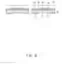
FIG. 1 is a schematic, cross-sectional view of an LED package according to an exemplary embodiment of the present disclosure.
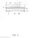
FIG. 2 is a schematic, cross-sectional view of an LED package according to an alternative embodiment of the present disclosure.
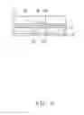
FIG. 3 is a schematic, cross-sectional view of an LED package according to an another alternative embodiment of the present disclosure.
FIGS. 4 to 8 show first to fifth steps of a method for manufacturing the LED package of FIG. 1, respectively.
DETAILED DESCRIPTION
Reference will now be made to the drawings to describe the exemplary embodiments in detail.
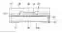
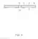
Referring to FIG. 1, an LED package in accordance with an exemplary embodiment of the present disclosure is illustrated. The LED package comprises a substrate 10, a first electrical portion 11 formed on a lateral side of the substrate 10, a second electrical portion 12 formed on an opposite lateral side of the substrate 10, a reflecting layer 13 formed on the substrate 10 between the first and second electrical portions 11, 12, an insulating block 14 covering the reflecting layer 13, two antioxidation layers 15 respectively formed on the first and second electrical portions 11, 12, an LED chip 16 mounted on the insulating block 14, and an encapsulant 17 covering the LED chip 16. The LED chip 16 is electrically connected to the first and second electrical portions 11, 12 respectively via two wires 18.
The substrate 10 is made of Al2O3, silicon, SiC, ceramic, polymer, or electrically insulting quartz. The substrate 10 has a top face 101 and a bottom face 102 opposite to the top face 101. The first electrical portion 11 and the second electrical portion 12 both extend from the top face 101 to the bottom face 102 of the substrate 10 along an outer edge of the substrate 10, whereby the LED package is formed as a surface mounting type device. The first electrical portion 11 is spaced from the second electrical portion 12.
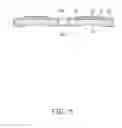
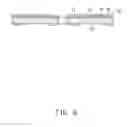
The reflecting layer 13 is formed on the top face 101 of the substrate 10 and is located between the first electrical portion 11 and the second electrical portion 12. The reflecting layer 13 is spaced from the first and second electrical portions 11, 12. The reflecting layer 13 is made of metal, such as silver, nickel, or alloy thereof. Alternatively, the reflecting layer 13a can further extend to the bottom face 102 of the substrate 10, as shown in FIG. 2.
The insulating block 14 cooperates with the substrate 10 to enclose the reflecting layer 13 therein. The insulating block 14 is made of electrically insulting and transparent material, such as silicone or SiO2.
The antioxidation layer 15 is formed by electroplating. The antioxidation layer 15 is made of noble metal which is highly resistant to oxidation and corrosion, such as Au (gold), Pt (platinum), or Ag (silver). In the exemplary embodiment of the disclosure, the antioxidation layers 15 are formed on top portions of the first and second electrical portions 11, 12. A top face of the insulating block 14 is coplanar with top faces of the antioxidation layers 15. It can be understood that, in an another alternative embodiment of the disclosure, another antioxidation layers 15b are formed on bottom portions of the first and second electrical portions 11, 12, as shown in FIG. 3. The antioxidation layers 15 are electrically attached on the first and second electrical portions 11, 12, respectively. The LED chip 16 is electrically connected to the two antioxidation layers 15 respectively via the two wires 18.
The encapsulant 17 is made of transparent materials, such as silicone, epoxy, quartz, or glass. The encapsulant 17 further comprises phosphors mixed therein, such as YAG, TAG, silicate, nitride, nitrogen oxides, phosphide, arsenide, telluride or sulfide. The phosphors are used for changing color of light from the LED chip 16 into a different color.
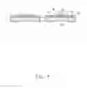
Referring to FIGS. 4-8, the disclosure provides a method for manufacturing the light emitting diode package in accordance with the exemplary embodiment of the disclosure.
Firstly, a substrate 10 is provided as shown in FIG. 4. The substrate 10 has a top face 101 and a bottom face 102. At least a first electrical portion 11 and a second electrical portion 12 are formed on the substrate 10. The first electrical portion 11 and the second electrical portion 12 extend from the top face 101 to the bottom face 102 of the substrate 10 along an outer edge of the substrate 10. A reflecting layer 13 is formed on the top face 101 of the substrate 10 between the first and second electrical portions 11, 12.
Then, as shown in FIG. 5, an insulating block 14 is provided to cover the reflecting layer 13. The insulating block 14 cooperates with the substrate 10 to enclose the reflecting layer 13 therein.
Then, as shown in FIG. 6, two antioxidation layers 15 are formed on the first electrical portion 11 and the second electrical portion 12, respectively, by electroplating.
Then, as shown in FIG. 7, at least an LED chip 16 is disposed on the insulating block 14. The LED chip 16 is electrically connected to the two antioxidation layers 15 respectively via two wires 18.
Then, as shown in FIG. 8, an encapsulant 17 is formed on the LED chip 16. The encapsulant 17 is made of transparent materials, such as silicone, epoxy, quartz, or glass. The encapsulant 17 can have phosphors doped therein.
It is to be understood, however, that even though multiple characteristics and advantages of the disclosure have been set forth in the foregoing description, together with details of the structure and function of the invention disclosure, the disclosure is illustrative only, and changes may be made in detail, especially in matters of shape, size, and arrangement of parts within the principles of the disclosure to the full extent indicated by the broad general meaning of the terms in which the appended claims are expressed.
Claims
What is claimed is:1. A light emitting diode (LED) package, comprising:
a substrate having a first electrical portion and a second electrical portion formed thereon;
two antioxidation layers formed on and electrically connected to the first electrical portion and the second electrical portion, respectively; and
an LED chip disposed on the substrate and electrically connected to the two antioxidation layers.
2. The LED package of claim 1, wherein the antioxidation layers are made of noble metal.
3. The LED package of claim 1, further comprising a reflecting layer formed on the substrate between the two antioxidation layers.
4. The LED package of claim 3, further comprising an insulating block covering the reflecting layer, wherein the insulating block cooperates with the substrate to enclose the reflecting layer therein.
5. The LED package of claim 4, wherein the LED chip is mounted on the insulating block.
6. The LED package of claim 4, wherein a top face of the insulating block is coplanar with top faces of the antioxidation layers.
7. The LED package of claim 3, wherein the reflecting layer extends from a top face of the substrate to a bottom face of the substrate.
8. The LED package of claim 1, wherein the first electrical portion and the second electrical portion extend from a top face of the substrate to a bottom face of the substrate.
9. The LED package of claim 8, wherein the two antioxidation layers formed on top portions of the first electrical portion and the second electrical portion, respectively.
10. The LED package of claim 9, further comprising another two antioxidation layers formed on bottom portions of the first electrical portion and the second electrical portion, respectively.
11. The LED package of claim 1, further comprising an encapsulant covering the LED chip.
12. A method for manufacturing a light emitting diode (LED) package comprising following steps:
providing a substrate having a first electrical portion and a second electrical portion formed thereon;
forming a reflecting layer on the substrate;
providing an insulating block covering the reflecting layer;
forming two antioxidation layers on the first electrical portion and the second electrical portion, respectively; and
providing an LED chip mounted on the insulating block and electrically connected to the first electrical portion and the second electrical portion.
13. The method of claim 12, wherein the antioxidation layers are made of metal which is resistant to oxidization and corrosion.
14. The method of claim 12, wherein a top face of the insulating block is coplanar with top faces of the antioxidation layers.
15. The method of claim 12, wherein the reflecting layer is attached on a top face of the substrate.
16. The method of claim 12, wherein the first electrical portion and the second electrical portion extend from a top face of the substrate to a bottom face of the substrate.
17. The method of claim 16, wherein the two antioxidation layers formed on top portions of the first electrical portion and the second electrical portion, respectively.
18. The method of claim 12, further comprising providing an encapsulant covering the LED chip.
19. The method of claim 12, wherein the insulating block cooperates with the substrate to enclose the reflecting layer therein.
20. The method of claim 12, wherein the antioxidation layers are formed by electroplating.
Images & Drawings included:
Sources:
- United States Patent and Trademark Office - verify current appl. status at the USPTO↗
Similar patent applications:
- » 20230064560
LIGHT EMITTING DIODE PACKAGE STRUCTURE, MANUFACTURING METHOD OF LIGHT EMITTING DIODE PACKAGE STRUCTURE AND LIGHT EMITTING PANEL - » 20080061458
Mold for forming lens of light emitting diode package and method of manufacturing light emitting diode package using the same - » 20110254039
LIGHT EMITTING DIODE PACKAGE, LIGHTING APPARATUS HAVING THE SAME, AND METHOD FOR MANUFACTURING LIGHT EMITTING DIODE PACKAGE - » 20240170468
Light Emitting Diode Package and Manufacturing Method of The Same, and Light Emitting Device - » 20100208468
Light emitting diode package, method for manufacturing the same and light source unit having the LED package - » 20080179612
Light-emitting diode package and manufacturing method thereof - » 20080076198
Method of manufacturing light emitting diode package and white light source module - » 20080179614
LIGHT-EMITTING DIODE PACKAGE AND MANUFACTURING METHOD THEREOF - » 20070158669
Chip coated light emitting diode package and manufacturing method thereof - » 20070212802
Method for manufacturing light emitting diode package
Recent applications in this class:
- » 20250063861 2025-02-20
LIGHT EMITTING MODULE HAVING LIGHT EMITTING DEVICE AND DISPLAY APPARATUS HAVING SAME - » 20250048800 2025-02-06
BASE MEMBER FOR LIGHT EMITTING DEVICE - » 20250040313 2025-01-30
LIGHT EMITTING DEVICE AND LIGHT EMITTING MODULE INCLUDING THE SAME - » 20250040311 2025-01-30
LED CIRCUIT BOARD AND LIGHT EMITTING MODULE - » 20250015235 2025-01-09
METHOD FOR ATTACHING MICRO LEDS TO DISPLAY BY USING FLUID AS SOFT LANDING MEDIUM FOR MICRO LEDS - » 20250006869 2025-01-02
LIGHT EMITTING DIODE PACKAGE AND METHOD OF MANUFACTURING THE SAME - » 20240429350 2024-12-26
OPTOELECTRONIC COMPONENT - » 20240413270 2024-12-12
SEMICONDUCTOR LIGHT-EMITTING APPARATUS - » 20240363809 2024-10-31
Display Device - » 20240363808 2024-10-31
OPTOELECTRONIC SEMICONDUCTOR COMPONENT AND PRODUCTION METHOD
Recent applications for this Assignee:
- » 20220252938 2022-08-11
Light emitting diode device, backlight module, and liquid crystal display device having same - » 20220077345 2022-03-10
Back plate and method for fluid-assisted assembly of micro-LEDs thereon - » 20210359153 2021-11-18
Back plate and method for fluid-assisted assembly of micro-LEDs thereon - » 20200326594 2020-10-15
Optical lens, backlight module and display device using same - » 20190326489 2019-10-24
Light emitting diode package - » 20190319173 2019-10-17
Side-view light emitting diode package structure - » 20190140136 2019-05-09
Manufacturing method for light emitting diode crystal grains using adhesive layer on auxiliary substrate to fill gaps between light emitting diode crystal grains - » 20190128951 2019-05-02
Detection method for light emitting diode chip - » 20190103512 2019-04-04
Light emitting diode structure - » 20190033659 2019-01-31
Liquid crystal display device