Double-groove bidirectional vertical component
US20120161200A1
2012-06-28
13/332,404
2011-12-21
✅ Patent granted
US 8,686,515 B2
2014-04-01
-
-
David Nhu
Wolf, Greenfield & Sacks, P.C.
2032-01-19
Abstract:
A mesa-type bidirectional vertical power component, including a substrate of a first conductivity type; a layer of the second conductivity type on each side of the substrate; first regions of the first conductivity type in each of the layers of the second conductivity type; and, at the periphery of each of its surfaces, two successive grooves, the internal groove crossing the layers of the second conductivity type, second doped regions of the first conductivity type being formed under the surface of the external grooves and having the same doping profile as the first regions.
Assignee:
- STMicroelectronics (Tours) SAS 271 🇫🇷 Tours, France
Applicant:
Interested in similar patents?
Get notified when new applications in this technology area are published.
Classification:
H01L29/0638 » CPC further
Semiconductor devices adapted for rectifying, amplifying, oscillating or switching, or capacitors or resistors with at least one potential-jump barrier or surface barrier, e.g. PN junction depletion layer or carrier concentration layer; Details of semiconductor bodies or of electrodes thereof; Multistep manufacturing processes therefor; Semiconductor bodies ; Multistep manufacturing processes therefor characterised by their shape; characterised by the shapes, relative sizes, or dispositions of the semiconductor regions ; characterised by the concentration or distribution of impurities within semiconductor regions characterised by particular constructional design considerations, e.g. for preventing surface leakage, for controlling electric field concentration or for internal isolations regions for preventing surface leakage or controlling electric field concentration for preventing surface leakage due to surface inversion layer, e.g. with channel stopper
H01L29/0661 » CPC further
Semiconductor devices adapted for rectifying, amplifying, oscillating or switching, or capacitors or resistors with at least one potential-jump barrier or surface barrier, e.g. PN junction depletion layer or carrier concentration layer; Details of semiconductor bodies or of electrodes thereof; Multistep manufacturing processes therefor; Semiconductor bodies ; Multistep manufacturing processes therefor characterised by their shape; characterised by the shapes, relative sizes, or dispositions of the semiconductor regions ; characterised by the concentration or distribution of impurities within semiconductor regions characterised by the shape of the body specially adapted for altering the breakdown voltage by removing semiconductor material at, or in the neighbourhood of, a reverse biased junction, e.g. by bevelling, moat etching, depletion etching
H01L29/66121 » CPC further
Semiconductor devices adapted for rectifying, amplifying, oscillating or switching, or capacitors or resistors with at least one potential-jump barrier or surface barrier, e.g. PN junction depletion layer or carrier concentration layer; Details of semiconductor bodies or of electrodes thereof; Multistep manufacturing processes therefor; Types of semiconductor device ; Multistep manufacturing processes therefor; Multistep manufacturing processes of devices having semiconductor bodies comprising group 14 or group 13/15 materials the devices being controllable only by variation of the electric current supplied or the electric potential applied, to one or more of the electrodes carrying the current to be rectified, amplified, oscillated or switched, e.g. two-terminal devices; Diodes Multilayer diodes, e.g. PNPN diodes
H01L29/66386 » CPC further
Semiconductor devices adapted for rectifying, amplifying, oscillating or switching, or capacitors or resistors with at least one potential-jump barrier or surface barrier, e.g. PN junction depletion layer or carrier concentration layer; Details of semiconductor bodies or of electrodes thereof; Multistep manufacturing processes therefor; Types of semiconductor device ; Multistep manufacturing processes therefor; Multistep manufacturing processes of devices having semiconductor bodies comprising group 14 or group 13/15 materials the devices being controllable only by the electric current supplied or the electric potential applied, to an electrode which does not carry the current to be rectified, amplified or switched, e.g. three-terminal devices; Thyristors Bidirectional thyristors
H01L29/747 » CPC further
Semiconductor devices adapted for rectifying, amplifying, oscillating or switching, or capacitors or resistors with at least one potential-jump barrier or surface barrier, e.g. PN junction depletion layer or carrier concentration layer; Details of semiconductor bodies or of electrodes thereof; Multistep manufacturing processes therefor; Types of semiconductor device ; Multistep manufacturing processes therefor controllable by only the electric current supplied, or only the electric potential applied, to an electrode which does not carry the current to be rectified, amplified or switched; Bipolar devices; Thyristor-type devices, e.g. having four-zone regenerative action Bidirectional devices, e.g. triacs
H01L29/87 » CPC main
Semiconductor devices adapted for rectifying, amplifying, oscillating or switching, or capacitors or resistors with at least one potential-jump barrier or surface barrier, e.g. PN junction depletion layer or carrier concentration layer; Details of semiconductor bodies or of electrodes thereof; Multistep manufacturing processes therefor; Types of semiconductor device ; Multistep manufacturing processes therefor controllable only by variation of the electric current supplied, or only the electric potential applied, to one or more of the electrodes carrying the current to be rectified, amplified, oscillated or switched; Diodes Thyristor diodes, e.g. Shockley diodes, break-over diodes
H01L29/76 IPC
Semiconductor devices adapted for rectifying, amplifying, oscillating or switching, or capacitors or resistors with at least one potential-jump barrier or surface barrier, e.g. PN junction depletion layer or carrier concentration layer; Details of semiconductor bodies or of electrodes thereof; Multistep manufacturing processes therefor; Types of semiconductor device ; Multistep manufacturing processes therefor controllable by only the electric current supplied, or only the electric potential applied, to an electrode which does not carry the current to be rectified, amplified or switched Unipolar devices, e.g. field effect transistors
H01L29/94 IPC
Semiconductor devices adapted for rectifying, amplifying, oscillating or switching, or capacitors or resistors with at least one potential-jump barrier or surface barrier, e.g. PN junction depletion layer or carrier concentration layer; Details of semiconductor bodies or of electrodes thereof; Multistep manufacturing processes therefor; Types of semiconductor device ; Multistep manufacturing processes therefor controllable only by variation of the electric current supplied, or only the electric potential applied, to one or more of the electrodes carrying the current to be rectified, amplified, oscillated or switched; Capacitors with potential-jump barrier or surface barrier Metal-insulator-semiconductors, e.g. MOS
H01L31/062 IPC
Semiconductor devices sensitive to infra-red radiation, light, electromagnetic radiation of shorter wavelength or corpuscular radiation and specially adapted either for the conversion of the energy of such radiation into electrical energy or for the control of electrical energy by such radiation; Processes or apparatus specially adapted for the manufacture or treatment thereof or of parts thereof; Details thereof adapted as photovoltaic [PV] conversion devices characterised by at least one potential-jump barrier or surface barrier the potential barriers being only of the metal-insulator-semiconductor type
H01L31/113 IPC
Semiconductor devices sensitive to infra-red radiation, light, electromagnetic radiation of shorter wavelength or corpuscular radiation and specially adapted either for the conversion of the energy of such radiation into electrical energy or for the control of electrical energy by such radiation; Processes or apparatus specially adapted for the manufacture or treatment thereof or of parts thereof; Details thereof in which radiation controls flow of current through the device, e.g. photoresistors characterised by at least one potential-jump barrier or surface barrier, e.g. phototransistors; Devices sensitive to infra-red, visible or ultra-violet radiation characterised by field-effect operation, e.g. junction field-effect phototransistor being of the conductor-insulator-semiconductor type, e.g. metal-insulator-semiconductor field-effect transistor
H01L31/119 IPC
Semiconductor devices sensitive to infra-red radiation, light, electromagnetic radiation of shorter wavelength or corpuscular radiation and specially adapted either for the conversion of the energy of such radiation into electrical energy or for the control of electrical energy by such radiation; Processes or apparatus specially adapted for the manufacture or treatment thereof or of parts thereof; Details thereof in which radiation controls flow of current through the device, e.g. photoresistors characterised by at least one potential-jump barrier or surface barrier, e.g. phototransistors; Devices sensitive to very short wavelength, e.g. X-rays, gamma-rays or corpuscular radiation characterised by field-effect operation, e.g. MIS type detectors
Description
CROSS REFERENCE TO RELATED APPLICATIONS
This application claims the priority benefit of French patent application number 10/61213, filed on Dec. 23, 2010, entitled DOUBLE-GROOVE BIDIRECTIONAL VERTICAL COMPONENT, which is hereby incorporated by reference to the maximum extent allowable by law.
BACKGROUND
1. Technical Field
Embodiments relate to vertical bidirectional power components, and more specifically to a bidirectional Shockley diode or a triac.
Two main types of bidirectional power components can be distinguished according to the technology used for their manufacturing: planar components and mesa components.
2. Discussion of the Related Art
FIG. 1 shows an example of a planar-type bidirectional Shockley diode. This device is formed in a lightly-doped N-type substrate 1 (with typically from 1014 to 1015 atoms/cm3). A P-type well 3 is formed on the upper surface side and a P-type well 5 is formed on the lower surface side. Usually, these wells are symmetrical and of same doping.
An N-type region 7 is formed in upper well 3 and an N-type region 9 is formed in lower well 5, regions 7 and 9 being heavily doped. Regions 7 and 9 are complementary in projection and substantially of the same surface area. As shown, regions 7 and 9 are generally interrupted by emitter short-circuits.
The component periphery, between the well limit and the chip edge, is coated with an insulating layer, respectively 11 at its upper surface and 13 at its lower surface. Also at the periphery of the structure, at the edge of the chip, heavily-doped N-type rings, respectively 15 at the upper surface and 16 at the lower surface, are used as a channel stop.
The upper surface is coated with a metallization A1 and the lower surface is coated with a metallization A2. When a positive voltage is applied on terminal A1, PNPN Shockley diode 3-1-5-9 is likely to turn on, when the breakdown voltage of the reverse junction between regions 1 and 5 is exceeded. When a positive voltage is applied to terminal A2, PNPN Shockley diode 5-1-3-7 is likely to turn on when the breakdown voltage of the reverse junction between regions 1 and 3 is exceeded.
To obtain breakdown voltage that is independent of the substrate doping and accurately define the volume of the breakdown areas, an N region 17 is arranged in front of upper N region 7 at the interface between well 3 and substrate 1 and an N region 19 is arranged in front of lower N region 9 at the interface between well 5 and substrate 1. N regions 17 and 19 will be called buried regions and for example result from implantations performed before the forming of P wells 3 and 5. Thus, junction J2 between N region 17 and P well 3 and junction J1 between P well 5 and N region 19 determine the breakdown voltages of the device. Optional P-type buried regions 21 and 23 have further been shown in front of N-type buried regions 19 and 17, respectively. Buried regions 21 and 23 aim at decreasing the effective thickness of substrate 1 in each of the Shockley diodes, to decrease the on-state resistance of the protection device.
A bidirectional Shockley diode of planar type such as shown in FIG. 1 provides satisfactory results. However, in many cases, it is preferred for technological reasons to form mesa-type diodes, especially because it is much simpler to form relatively deep P regions (more than 30 μm deep for diodes adapted to breakdown voltages ranging from 50 to 400 V) with no masking.
FIG. 2 shows an example of a mesa-type bidirectional Shockley diode. To simplify the description, layers similar to that in FIG. 1 have been designated with the same reference numerals. An essential difference is that, instead of forming local P-type wells 3 and 5 on either side of the substrate, uniform P-type layers, also designated with reference numerals 3 and 5, are formed with no masking on both surfaces of the substrate. The diode is delimited by peripheral grooves, respectively 31 on the upper surface side and 33 on the lower surface side, filled with an appropriate insulating material, respectively 35 and 37, currently a glassivation. The grooves cut the junctions between the substrate and P layers 3, 5.
Generally, as compared with a planar-type diode, a mesa-type bidirectional Shockley diode, biased to a voltage smaller than its breakdown voltage, has greater leakage currents. Further, the leakage currents tend to increase during the lifetime of the component when it is submitted to external stress, such as a lengthy biasing and a high temperature. In FIG. 2, equipotential line VA2 when a positive potential difference (VA2-VA1) is applied between electrodes A2 and A1 has been illustrated with bold dotted lines. The technology used to create the mesa groove, its specific geometric shape and the nature of the passivating materials explain the distribution of the equipotential lines at the edges of the component as well as their variation in the presence of stress. The electric field thus present at the passivation-silicon interfaces is responsible for the high leakage currents.
Many solutions and mesa-type bidirectional Shockley diode structures have been provided to overcome these disadvantages. However, all known solutions are relatively complex and require additional manufacturing steps with respect to those required for the manufacturing of a component such as that illustrated in FIG. 2. The same problems are posed for triacs.
There thus is a need for a simple mesa-type vertical bidirectional power component with a low leakage current, that remains steady along time.
SUMMARY
Thus, an embodiment provides a mesa-type bidirectional vertical power component which is easy to form and which has low leakage currents, steady along time.
More specifically, an embodiment aims at forming such a vertical bidirectional power component without using steps of a different type than the steps used to manufacture a conventional mesa component such as the bidirectional Shockley diode of FIG. 2.
An embodiment provides a mesa-type bidirectional vertical power component, comprising a substrate of a first conductivity type; a layer of the second conductivity type on each side of the substrate; first regions of the first conductivity type in each of the layers of the second conductivity type; and, at the periphery of each of its surfaces, two successive grooves, the internal groove crossing the layers of the second conductivity type, second doped regions of the first conductivity type being formed under the surface of the external grooves and having the same doping profile as the first regions.
According to an embodiment, the surface area of the space between two grooves is taken up by a portion of said layer of the second conductivity type.
According to an embodiment, the first conductivity type is type N and the second conductivity type is type P.
According to an embodiment, the component is a bidirectional Shockley diode.
According to an embodiment, the component comprises a buried region of the first conductivity type under each of said regions of the first conductivity type, at the interface between the substrate and the corresponding layer of the second conductivity type, each buried region being complementary in projection with the other.
According to an embodiment, the component comprises buried regions of the second conductivity type at the interfaces between layers and substrate in front of the buried regions of the first conductivity type.
An embodiment provides a method for manufacturing a component such as hereabove, comprising the steps of:
forming a layer of the second conductivity type on both sides of a semiconductor substrate of the first conductivity type;
forming a first groove at the external periphery of the component;
forming layers of the first conductivity type at the locations operational for the power component and at the level of the first groove;
forming a second groove at the periphery of the component, internally with respect to the first groove.
According to an embodiment, the method further comprises the steps of:
-
- filling the grooves with a passivation material; and
- forming upper and lower metallizations.
The foregoing and other objects, features, and advantages will be discussed in detail in the following non-limiting description of specific embodiments in connection with the accompanying drawings.
BRIEF DESCRIPTION OF THE DRAWINGS
FIG. 1, previously described, is a simplified cross-section view of a planar-type bidirectional Shockley diode;
FIG. 2, previously described, is a simplified cross-section view of a mesa-type bidirectional Shockley diode;
FIG. 3 is a simplified cross-section view of a bidirectional Shockley diode according to an embodiment; and
FIGS. 4A to 4F are partial cross-section views illustrating successive steps of the manufacturing of a vertical bidirectional power component such as in FIG. 3.
For clarity, the same elements have been designated with the same reference numerals in the different drawings and, further, as usual in the representation of electronic components, the various drawings are not to scale.
DETAILED DESCRIPTION
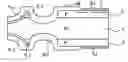
FIG. 3 is a simplified view of a vertical bidirectional component. This component comprises elements common with the bidirectional Shockley diode of FIG. 2.
Thus, the component comprises, on the upper side of a substrate 1, a P-type layer 3 formed with no masking and, on the lower side of the substrate, a P-type layer 5 also formed with no masking. In layer 3 is formed an N-type region 7, generally provided with emitter short-circuits, as shown, and in layer 5 is formed an N-type layer 9 also comprising emitter short-circuits. Layer 7 and 9 are substantially complementary in projection. Layers 3 and 7 are coated with an upper surface metallization A1 and layers 5 and 9 are coated with a lower surface metallization A2. If the bidirectional component of FIG. 3 is intended to form a bidirectional Shockley diode, it will further comprise buried layers 17 and 19 such as illustrated in FIG. 2. If it is intended to form a triac, it will further comprise a gate area, not shown.
The component is surrounded with a first groove, respectively 40 on the upper surface and 42 on the lower surface, and with a second external groove (half a groove remaining after sawing), respectively 44 on the upper surface and 46 on the lower surface. Given that, as discussed previously, P-type layers 3 and 5 have been formed with no masking, there remain portions of P layer 3-1 and 5-1 in the surface of the substrate portion between the two grooves. Further, at the same time as heavily-doped N-type regions 7 and 9 have been formed, respectively, N-type regions 7-1 and 9-1 which cover the intermediary area between the two grooves and the surface of the external grooves have been formed.
Thus, there remain N-type rings, respectively 7-1 on the upper surface side and 9-1 on the lower surface side, at the component periphery, and these rings prevent equipotential line VA2 from extending beyond these N-type regions. Thus, this equipotential line cannot reach the lateral periphery of the components, which would risk causing the occurrence of non-negligible leakage currents, variable along time.
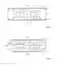
FIGS. 4A to 4F are cross-section views illustrating an embodiment of a component such as that in FIG. 3. In this series of drawings, an enlargement of the left-hand portion of a component separated from its neighbors has been shown. It should be clear that a component assembly is in fact formed by the steps described in relation with FIGS. 4A to 4F on a silicon wafer and that only at the end of the process is the wafer sawn to separate the components from one another.
At the step illustrated in FIG. 4A, P regions 3 and 5 have been formed with no masking, respectively on the upper surface side and on the lower surface side of a substrate 1.
At the step illustrated in FIG. 4B, first grooves which correspond to grooves 44 and 46 of FIG. 3 have been formed, on both sides of the wafer.
At the step illustrated in FIG. 4C, N-type regions 7 have been formed, for example, by implantation, to form an upper surface cathode region of the component. The implantation mask is selected to simultaneously form regions 7-1 at the periphery, especially in the region where peripheral groove 44 has been formed. Simultaneously, or in a subsequent step, lower surface N-type cathode regions 9 are formed and regions 9-1 are simultaneously formed at the component periphery and especially at the level of groove 46.
At the step illustrated in FIG. 4D, grooves 40, 42 have been formed at the periphery but towards the inside with respect to grooves 44, 46. Grooves 40, 42 are sufficiently deep to eliminate the portions of P layers 3 and 5 located at the periphery. There however remain P-type surface regions 3-1 and 5-1 in the substrate portion remaining between grooves 40 and 44 on the one hand, and 42 and 46 on the other hand.
At the step illustrated in FIG. 4E, passivations, currently glassivations, 48 and 50 intended to protect the grooves have been formed.
Finally, at the step illustrated in FIG. 4F, anode and cathode metallizations A1 and A2 have been formed.
This step sequence has thus effectively provided a component corresponding to that illustrated in FIG. 3.
It should be noted that this step sequence comprises no step of a different nature than the steps used to form the component of FIG. 2. Only one additional step is provided: the forming of an additional groove.
Such a structure avoids a spreading of the equipotential lines to the component periphery. The equipotential lines stop at most at the level of heavily-doped N-type regions 7-1 and 9-1 in the peripheral area of the component.
As an example of dimensions, the internal groove may have a width of 120 μm, the external half-groove having a 50-μm width, and a guard distance of 40 μm is provided for each of the grooves, between the two grooves. The peripheral protection then has a general extension of 250 μm. In a conventional mesa device such as that in FIG. 2, in which only one peripheral half-groove is provided, this half-groove has a width which ranges from 125 μm for the lowest breakdown voltages (50 V) to 225 μm for the highest breakdown voltages (1000 V for a triac). If the active portion of the chip has a dimension on the order of 2×2 or 3×3 mm2, it can be observed that the size increase of the peripheral protection ranges from approximately 3% to approximately 20%. The resulting cost increase is, even in the worst case, lower than the cost increase which would result from the passing from a mesa structure to a planar structure (with the need to mask the P drive-in).
Specific embodiments of the present invention have been described. Various alterations and modifications will occur to those skilled in the art, especially as concerns the thicknesses of the various layers and the doping levels, which will be adapted to the desired breakdown voltages which will preferably range between 50 and 1000 volts.
On the other hand, a component similar to that described herein may be formed by inverting all the conductivity types of the various layers.
Such alterations, modifications, and improvements are intended to be part of this disclosure, and are intended to be within the spirit and the scope of the present invention. Accordingly, the foregoing description is by way of example only and is not intended to be limiting. The present invention is limited only as defined in the following claims and the equivalents thereto.
Claims
What is claimed is:1. A mesa-type bidirectional vertical power component, comprising:
a substrate of a first conductivity type;
a layer of the second conductivity type on each side of the substrate;
first regions of the first conductivity type in each of the layers of the second conductivity type;
and further comprising, at the periphery of each of its surfaces, two successive grooves, the internal groove crossing the layers of the second conductivity type, second doped regions of the first conductivity type being formed under the surface of the external grooves and having the same doping profile as the first regions.
2. The component of claim 1, wherein the surface area of the space between two grooves is taken up by a portion of said layer of the second conductivity type.
3. The component of claim 1, wherein the first conductivity type is type N and the second conductivity type is type P.
4. The component of claim 1, forming a bidirectional Shockley diode.
5. The component of claim 4, comprising a buried region of the first conductivity type under each of said regions of the first conductivity type, at the interface between the substrate and the corresponding layers of the second conductivity type, each buried region being complementary in projection with the other.
6. The component of claim 5, comprising buried regions of the second conductivity type, at the interfaces between layers and substrate in front of the buried regions of the first conductivity type.
7. A method for manufacturing the component of claim 1, comprising the steps of:
forming a layer of the second conductivity type on both sides of a semiconductor substrate of the first conductivity type;
forming a first groove at the external periphery of the component; forming layers of the first conductivity type at the locations operational for the power component and at the level of the first groove;
forming a second groove at the periphery of the component, internally with respect to the first groove.
8. The method of claim 7, further comprising the steps of:
filling the grooves with a passivation material; and
forming upper and lower metallizations.
Images & Drawings included:

Sources:
- United States Patent and Trademark Office - verify current appl. status at the USPTO↗
Recent applications in this class:
- » 20230420576 2023-12-28
Transient voltage suppression device - » 20230411535 2023-12-21
Silicon-controlled rectifiers for electrostatic discharge protection - » 20230361223 2023-11-09
Snapback electrostatic discharge protection device with tunable parameters - » 20220262960 2022-08-18
Power semiconductor component for voltage limiting, arrangement having two power semiconductor components, and a method for voltage limiting - » 20220045222 2022-02-10
Semiconductor device and a method of manufacture of a semiconductor device - » 20180145186 2018-05-24
Packaged overvoltage protection circuit for triggering thyristors - » 20180097124 2018-04-05
Semiconductor device and method of forming the same - » 20170278982 2017-09-28
Diode - » 20170222063 2017-08-03
Semiconductor structure and method for manufacturing the same - » 20160268447 2016-09-15
Data transmission system
Recent applications for this Assignee:
- » 20250191935 2025-06-12
MANUFACTURING METHOD OF RF COMPONENTS - » 20250169151 2025-05-22
SEMICONDUCTOR TRIODE - » 20240275298 2024-08-15
VOLTAGE CONVERTER - » 20240204112 2024-06-20
THIN DIODES - » 20240194666 2024-06-13
OVERVOLTAGE PROTECTION DEVICE - » 20240128311 2024-04-18
METHOD OF FABRICATING A CAPACITOR - » 20240113704 2024-04-04
CIRCUIT AND METHOD FOR CONTROLLING A TRANSISTOR - » 20240088885 2024-03-14
TRANSISTOR CONTROL CIRCUIT - » 20240063162 2024-02-22
DIE WITH METAL PILLARS - » 20240022242 2024-01-18
Thyristor control device