Manufacturing method of printing circuit board with micro-radiators
US20120329183A1
2012-12-27
13/514,999
2011-01-06
✅ Patent granted
US 9,185,791 B2
2015-11-10
WO; PCT/CN2011/070051; 20110106
WO; WO2012/083595; 20120628
Savitr Mulpuri
2031-10-11
Abstract:
The present invention relates to a manufacturing method of a printing circuit board. The manufacturing method mainly includes: forming one or more cylindrical micro-radiators by cutting a high conductive and electrical insulating substrate according to predetermined size; manufacturing one or more mounting holes in copper clad plates and prepregs; embedding the cylindrical micro-radiators into the mounting holes. The present invention combines the micro-radiator with high thermal conductivity and traditional stiffness printing circuit board. The printing circuit board with micro-radiators has the advantages of high thermal conductivity and stable heat transfer, and also has the advantages of routing flexibility and reliable electrical connections.
Assignee:
- RAYBEN TECHNOLOGIES (ZHUHAI) LIMITED 4 🇨🇳 Zhuhai, China
Applicant:
Interested in similar patents?
Get notified when new applications in this technology area are published.
Classification:
H05K2201/0187 » CPC further
Indexing scheme relating to printed circuits covered by; Dielectrics; Dielectric layers with regions of different dielectrics in the same layer, e.g. in a printed capacitor for locally changing the dielectric properties
H05K2201/0187 » CPC further
Indexing scheme relating to printed circuits covered by; Dielectrics; Dielectric layers with regions of different dielectrics in the same layer, e.g. in a printed capacitor for locally changing the dielectric properties
H05K1/0204 » CPC main
Printed circuits; Details; Thermal arrangements, e.g. for cooling, heating or preventing overheating; Cooling of mounted components using means for thermal conduction connection in the thickness direction of the substrate
H05K1/0204 » CPC main
Printed circuits; Details; Thermal arrangements, e.g. for cooling, heating or preventing overheating; Cooling of mounted components using means for thermal conduction connection in the thickness direction of the substrate
H01L33/642 » CPC further
Semiconductor devices with at least one potential-jump barrier or surface barrier specially adapted for light emission; Processes or apparatus specially adapted for the manufacture or treatment thereof or of parts thereof; Details thereof characterised by the semiconductor body packages; Heat extraction or cooling elements characterized by the shape
H05K3/4623 » CPC further
Apparatus or processes for manufacturing printed circuits; Manufacturing multilayer circuits by laminating two or more circuit boards the circuit boards having internal via connections between two or more circuit layers before lamination, e.g. double-sided circuit boards
H05K3/4623 » CPC further
Apparatus or processes for manufacturing printed circuits; Manufacturing multilayer circuits by laminating two or more circuit boards the circuit boards having internal via connections between two or more circuit layers before lamination, e.g. double-sided circuit boards
H05K2201/10106 » CPC further
Indexing scheme relating to printed circuits covered by; Details of components or other objects attached to or integrated in a printed circuit board; Types of components Light emitting diode [LED]
H05K2201/10106 » CPC further
Indexing scheme relating to printed circuits covered by; Details of components or other objects attached to or integrated in a printed circuit board; Types of components Light emitting diode [LED]
H05K2203/063 » CPC further
Indexing scheme relating to apparatus or processes for manufacturing printed circuits covered by; Lamination of preperforated insulating layer
H05K2203/063 » CPC further
Indexing scheme relating to apparatus or processes for manufacturing printed circuits covered by; Lamination of preperforated insulating layer
H01L33/62 IPC
Semiconductor devices with at least one potential-jump barrier or surface barrier specially adapted for light emission; Processes or apparatus specially adapted for the manufacture or treatment thereof or of parts thereof; Details thereof characterised by the semiconductor body packages Arrangements for conducting electric current to or from the semiconductor body, e.g. lead-frames, wire-bonds or solder balls
H01L33/64 IPC
Semiconductor devices with at least one potential-jump barrier or surface barrier specially adapted for light emission; Processes or apparatus specially adapted for the manufacture or treatment thereof or of parts thereof; Details thereof characterised by the semiconductor body packages Heat extraction or cooling elements
H05K1/02 IPC
Printed circuits Details
H05K1/02 IPC
Printed circuits Details
H05K3/46 IPC
Apparatus or processes for manufacturing printed circuits Manufacturing multilayer circuits
H05K3/46 IPC
Apparatus or processes for manufacturing printed circuits Manufacturing multilayer circuits
Description
FIELD OF THE INVENTION
The present invention relates to printing circuit boards, particularly, the present invention relates to a manufacturing method of a printing circuit board with micro-radiators.
BACKGROUND OF THE INVENTION
Printing circuit boards (PCBs) are one of important elements in electronics industry. PCBs are used as mechanical support elements for the electronic components, and realize electrical connection among the electronic components. In addition, graphics and numbers of the components can be printed on the PCBs, it is convenient for furnishing, checking or maintaining the components. The PCBs are used in almost every electronic device, such as electronic watch, calculator, computer, communication electronics device, military weapon systems.
Traditional PCBs are plated through hole structure, insulation material among layers is FR4 material, the thermal conductivity of the insulation material is 0.4 W/mk. In recent years, the thermal conductivity of the insulation material is 1.3-2.2 W/mk. When plenty of integrated circuits (especially high power LED) are installed on the printing circuit board, the thermal conductivity of the printing circuit board come up to tens or hundreds of W/mk. Obviously, it is far beyond the thermal conductivity of the insulation material of the prior art.
Therefore, there are some shortcomings in the prior art.
SUMMARY OF THE INVENTION
An object of the present invention is to provide a manufacturing method of the printing circuit board with micro-radiators.
The object of the present invention is realized by use the technical solutions as follows:
A manufacturing method of a printing circuit board with micro-radiators includes:
providing a board comprising a thermal conductive and electrical insulating base and copper foils over an upper surface and a lower surface of the board, and forming one or more cylindrical micro-radiators by cutting the board according to predetermined size;
providing single-sided or double-sided copper clad plates and prepregs, forming joined boards by cutting the copper clad plates and prepregs according to predetermined size, and manufacturing inner circuit in the copper clad plates;
manufacturing one or more mounting holes in copper clad plates and prepregs, the shape and size of the mounting holes adapting to the cylindrical micro-radiators;
laminating the copper clad plates and the prepregs, a top layer and a bottom layer being copper clad plates, embedding the cylindrical micro-radiators into the mounting holes;
pressing the copper clad plates and the prepregs;
laminate drilling and electroplating, etching, solder masking and tinning, then being silkscreened and mounting heating elements on an upper surface of micro-radiators.
Compared with the prior art, the present invention combines the micro-radiators with high thermal conductivity and traditional rigid printing circuit board. The printing circuit board with micro-radiators has the advantages of high thermal conductivity and stable heat transfer, and also has the advantages of routing flexibility and reliable electrical connections. The heat coming from the heating elements can be conducted out of the printing circuit board in time and effectively. The printing circuit board with micro-radiators is the ideal carrier board for the heating element and heating element array. The manufacturing method of the printing circuit board with micro-radiators has the advantages of simplicity and strong practicability.
DETAILED DESCRIPTION OF THE DRAWINGS
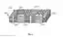
FIG. 1 is a schematic cross-sectional view illustrating the printing circuit board with micro-radiators of the present invention.
FIG. 2 is a flowchart of the manufacturing method of the printing circuit board with micro-radiators of FIG. 1.
DETAILED DESCRIPTION OF THE PREFERRED EMBODIMENT
As shown in FIG. 1, the printing circuit board is a rigid PCB, and includes a substrate. The substrate consists of 3 layers of copper clad plates 110 and 2 layers of prepregs 120. The 3 layers of copper clad plates 110 and the 2 layers of prepregs 120 are cross-laminated. A top layer and a bottom layer are copper clad plates 110. An upper surface and a lower surface of each copper clad plate 110 are covered copper circuit 130. The printing circuit board also includes a plurality of cylindrical micro-radiators 150, each cylindrical micro-radiator 150 is embedded into a cylindrical hole of the substrate. The height of the micro-radiator 150 is equal to the thickness of the substrate. An upper surface 151 and a lower surface 152 of the micro-radiator are covered by copper foils. A LED chip 160 is installed on the upper surface 151, and the power signal input of the LED chip 160 is electrically connected to the inner circuit of the printing circuit board, and the lower surface 152 of the micro-radiator 150 is insulated from other circuits of the printing circuit board.
A base of micro-radiator 150 is made from electrical insulating material, such as alumina ceramic, aluminum nitride ceramic, silicon carbide, diamond, and so on. The thermal conductivity between the upper surface 151 and the lower surface 152 of the micro-radiator 150 can be achieved to 20-1000 W/mk.
When the LED chip 160 is operating, the LED is lighting and emitting heat continuously. The heat is transferred from the upper surface 151 to the lower surface 152 of the micro-radiator 150 by the thermal conductive base, then transferred out of the printing circuit board by copper foil of the lower surface 152.
As shown in FIG. 2, the manufacturing method of the printing circuit board of FIG. 1 includes the following steps:
A210: providing a board with a high conductive and electrical insulating base, and forming a plurality of cylindrical micro-radiators by cutting the board according to predetermined size.
The upper surface and the lower surface of the base are covered by copper foils. The upper surface 151 and the lower surface 152 of each cylindrical micro-radiator are covered by copper foils.
The base is made from electrical insulating material, such as alumina ceramic, aluminum nitride ceramic, silicon carbide, diamond, and so on.
A220: providing 3 layers of copper clad plates and 2 layers of prepregs, forming joined boards, and manufacturing inner circuit in the copper clad plates.
Forming joined boards of PCB is by cutting the 3 layers of copper clad plates 110 and 2 layers of prepregs according to predetermined size. Manufacturing inner circuit is by using traditional pattern transfer method.
A230: manufacturing a plurality of mounting holes in copper clad plates and prepregs.
Manufacturing a plurality of mounting holes can be using probing, milling, punching, and so on. The shape and size of the mounting hole adapts to cylindrical micro-radiator 150.
A240: laminating the copper clad plates and the prepregs, and the top layer and the bottom layer being copper clad plates, and embedding the cylindrical micro-radiators into the mounting holes.
Laminating the copper clad plates 110 and the prepregs is by using traditional laminating method of multi-layer PCBs.
A250: pressing the copper clad plates and the prepregs.
Pressing the copper clad plates 110 and the prepregs is by using traditional pressing method of multi-layer PCBs.
A260: laminate drilling and electroplating, etching, solder masking and tinning, then being silkscreened and mounting heating elements 160 on an upper surface 151 of micro-radiators 150.
Copper foil over an upper surface of the base is electrically connected to the inner circuit, and copper foil over a lower surface of the base is electrically insulated from the inner circuit.
The manufacturing method of the present invention is not limited by the preferred embodiments, all the equivalent change and modification according to the present invention are covered by the protection scope of the claims. For example:
In step A260, one or more heating element such as LED elements or integrated circuit chip can be installed on the upper surface 151 of the micro-radiators 150.
In step A220, the number of the copper clad plates 110 can be N(N>1), the number of the prepregs can be N−1, and the number of the layers of the printing circuit board is 2N−1.
In step A220, the single-sided or double-sided copper clad plates are provided. If the single-sided copper clad plates are provided, both a top surface and a bottom surface of the multi-layer printing circuit board should be copper clad during the process of pressing the copper clad plates and the prepregs.
In step A210, the micro-radiator is elliptic cylindrical, cube-shaped or cylinder shape, when the micro-radiator is cylinder shape, both the upper surface and the lower surface are rhombus, triangle or trapezoid. The number of the micro-radiators depends on the need of the actual circuit, it can be one or more.
Heating elements are electrically connected to the inner or outer circuit of the printing circuit board.
Claims
1. A manufacturing method of a printing circuit board with micro-radiators, including:
providing a board comprising a thermal conductive and electrical insulating base and copper foils over an upper surface and a lower surface of the board, and forming one or more cylindrical micro-radiators by cutting the board according to predetermined size;
providing single-sided or double-sided copper clad plates and prepregs forming joined boards by cutting the copper clad plates and prepregs according to predetermined size, and manufacturing inner circuit in the copper clad plates;
manufacturing one or more mounting holes in copper clad plates and prepregs, the shape and size of the mounting holes adapting to the cylindrical micro-radiators;
laminating the copper clad plates and the prepregs, a top layer and a bottom layer being copper clad plates, embedding the cylindrical micro-radiators into the mounting holes;
pressing the copper clad plates and the prepregs;
laminate drilling and electroplating, etching, solder masking and tinning, then being silkscreened and mounting heating elements on an upper surface of micro-radiators.
2. The manufacturing method of the printing circuit board of claim 1, wherein, the micro-radiator is elliptic cylindrical, cube-shaped or cylinder shape, when the micro-radiator is cylinder shape, both the upper surface and the lower surface are rhombus, triangle or trapezoid.
3. The manufacturing method of the printing circuit board of claim 1, wherein, the thermal conductive and electrical insulating base is made from alumina ceramic, aluminum nitride ceramic, silicon carbide, or diamond.
4. The manufacturing method of the printing circuit board of claim 1, wherein the copper foil over an upper surface of the micro-radiator is electrically connected to the inner or outer circuit, and the copper foil over a lower surface of the micro-radiator is electrically insulated from the inner and outer circuit.
5. The manufacturing method of the printing circuit board of claim 1, wherein both a top surface and a bottom surface of the multi-layer printing circuit board are copper clad.
6. The manufacturing method of the printing circuit board of claim 1, wherein the heating elements are LED chips.
7. The manufacturing method of the printing circuit hoard of claim 1, wherein manufacturing one or more mounting holes can be using probing, milling, or punching.
8. The manufacturing method of the printing circuit board of claim 1, wherein the number of the copper clad plates can be N, the number of the prepregs can be N−1, and the number of the layers of the printing circuit board is 2N−1.
Images & Drawings included:


Sources:
- United States Patent and Trademark Office - verify current appl. status at the USPTO↗
Similar patent applications:
Recent applications in this class:
- » 20250294666 2025-09-18
EXPANSION CARD MODULE - » 20250240869 2025-07-24
ELECTRONIC DEVICE - » 20250240868 2025-07-24
Printed circuit board assembly - » 20250240867 2025-07-24
Thermal Management Enhancement of Electronic Components - » 20250234452 2025-07-17
MODULE-LEVEL THERMAL MANAGEMENT MECHANISM - » 20250203752 2025-06-19
PRINTED CIRCUIT BOARD, METAL-CERAMIC SUBSTRATE AS AN INSERT, AND METHOD FOR MANUFACTURING A PRINTED CIRCUIT BOARD - » 20250185151 2025-06-05
HEAT DISSIPATION SUBSTRATE, HEAT DISSIPATION CIRCUIT BOARD, HEAT DISSIPATION MEMBER, AND METHOD FOR MANUFACTURING HEAT DISSIPATION SUBSTRATE - » 20250168964 2025-05-22
HEAT DISSIPATING ASSEMBLY FOR CIRCUIT - » 20250089153 2025-03-13
SOLID STATE TRANSFORMER AND STACK-UP STRUCTURE OF PRINTED CIRCUIT BOARD THEREOF - » 20250081327 2025-03-06
NON-CONTACT COOLING ASSEMBLY FOR COOLING SUBSTRATES
Recent applications for this Assignee:
- » 20190355644 2019-11-21
Insulated gate bipolar transistor module and manufacturing method thereof - » 20190198424 2019-06-27
POWER MODULE WITH BUILT-IN POWER DEVICE AND DOUBLE-SIDED HEAT DISSIPATION AND MANUFACTURING METHOD THEREOF - » 20190198423 2019-06-27
DEVICE MODULE EMBEDDED WITH SWITCH CHIP AND MANUFACTURING METHOD THEREOF