MEMORY DEVICE
US20130097361A1
2013-04-18
13/286,167
2011-10-31
Abstract:
A memory device includes a control part and a storage part. The control part includes a first interface, a second interface, and a storage controller. The first interface is connected to an electronic device through a first bus. The second interface is connected to the storage controller through a second bus. The storage part includes a third interface and a storage unit. The storage unit is connected to the third interface through a third bus. The control part and the storage part are connected through a connection of the second interface and the third interface.
Assignee:
- HON HAI PRECISION INDUSTRY CO., LTD. 12,828 🇹🇼 Tu-Cheng, Taiwan
- HONG FU JIN PRECISION INDUSTRY (SHENZHEN) CO., LTD. 4,225 🇨🇳 Shenzhen City, China
Interested in similar patents?
Get notified when new applications in this technology area are published.
Classification:
G06F3/0607 » CPC main
Input arrangements for transferring data to be processed into a form capable of being handled by the computer; Output arrangements for transferring data from processing unit to output unit, e.g. interface arrangements; Digital input from, or digital output to, record carriers, e.g. RAID, emulated record carriers or networked record carriers; Interfaces specially adapted for storage systems specifically adapted to achieve a particular effect; Improving or facilitating administration, e.g. storage management by facilitating the process of upgrading existing storage systems, e.g. for improving compatibility between host and storage device
G06F3/0658 » CPC further
Input arrangements for transferring data to be processed into a form capable of being handled by the computer; Output arrangements for transferring data from processing unit to output unit, e.g. interface arrangements; Digital input from, or digital output to, record carriers, e.g. RAID, emulated record carriers or networked record carriers; Interfaces specially adapted for storage systems making use of a particular technique; Vertical data movement, i.e. input-output transfer; data movement between one or more hosts and one or more storage devices Controller construction arrangements
G06F3/0679 » CPC further
Input arrangements for transferring data to be processed into a form capable of being handled by the computer; Output arrangements for transferring data from processing unit to output unit, e.g. interface arrangements; Digital input from, or digital output to, record carriers, e.g. RAID, emulated record carriers or networked record carriers; Interfaces specially adapted for storage systems adopting a particular infrastructure; In-line storage system; Single storage device Non-volatile semiconductor memory device, e.g. flash memory, one time programmable memory [OTP]
G06F12/00 IPC
Accessing, addressing or allocating within memory systems or architectures
Description
BACKGROUND
1. Technical Field
The present disclosure relates to an memory device, especially relates to a memory device which can be separated to two parts.
2. Description of Related Art
Referring to FIG. 1, a conventional Solid State Disk (SSD) 10 includes a flash controller 101 and flash chips 102. The flash controller 101 and the flash chips 102 are connected through a flash bus 103. Due to the flash controller 101 and the flash chips 102 cannot be separated, damage to either the flash controller 101 or the flash chips 102 will render the SSD 10 unusable, thus results in unnecessary waste.
BRIEF DESCRIPTION OF THE DRAWINGS
The components of the drawings are not necessarily drawn to scale, the emphasis instead being placed upon clearly illustrating the principles of the present disclosure. Moreover, in the drawings, like reference numerals designate corresponding parts throughout several views.
FIG. 1 is a block diagram of a Solid State Disk in related art.
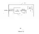
FIG. 2 is a block diagram of a memory device in accordance with an exemplary embodiment.
DETAILED DESCRIPTION
Referring to FIG. 2, a memory device 1 includes a control part 11 and a storage part 12. The control part 11 includes a first interface 111, a second interface 112, and a storage controller 113. The memory device 1 is connected to an electronic device (not shown) through the first interface 111. The first interface 111 is connected to the storage controller 113 through a first bus 114. The second interface 112 is connected to the storage controller 113 through a second bus 115.
The storage part 12 includes a third interface 121 and a storage unit 122. The storage unit 122 is connected to the third interface 121 through a third bus 121.
The control part 11 and the storage part 12 are connected through a connection of the second interface 112 and the third interface 121. The storage controller 113 controls the storage unit 122 of the storage part 12 to read and write data. Thus, when the storage part 12 is broken, the broken storage part 12 can be replaced with a new one, and the control part 11 can continue to be used , or when the control part 11 is broken, the broken control part 11 can be replaced with a new one, and the storage part 12 can continue to be used.
In the present embodiment, the storage device 1 is a SSD. The first interface 111 is a Serial Advanced Technology Attachment (SASA) interface. The storage unit 122 is a flash memory. The first bus 114 is a SASA bus. The second bus 115 and the third bus 123 are flash bus.
In the present embodiment, the second interface 112 and the third interface 121 includes data signal pins, address signal pins, control signals pins, and a ground signal pin.
Although, the present disclosure has been specifically described on the basis of preferred embodiments, the disclosure is not to be construed as being limited thereto. Various changes or modifications may be made to the embodiment without departing from the scope and spirit of the disclosure.
Claims
What is claimed is:1. A memory device comprising:
a control part comprising a first interface, a second interface and a storage controller, wherein the first interface is connected to an electronic device through a first bus, and the second interface is connected to the storage controller through a second bus; and
a storage part comprising a third interface and a storage unit, wherein the storage unit is connected to the third interface through a third bus;
wherein the control part and the storage part are connected through a connection of the second interface and the third interface.
2. The memory device as described in claim 1, wherein the memory device is a Solid State Disk.
3. The memory device as described in claim 1, wherein the storage unit is a flash memory.
4. The memory device as described in claim 1, wherein the second bus and the third bus are flash bus.
Images & Drawings included:


Sources:
- United States Patent and Trademark Office - verify current appl. status at the USPTO↗
Similar patent applications:
- » 20170206978
Flash memory device revising program voltage, three-dimensional memory device, memory system including the memory device, and methods of programming the memory device - » 20120039132
Memory device, systems and devices including a memory device, methods of operating a memory device, and/or methods of operating systems and devices including a memory device - » 20120056151
Memory devices, memory device constructions, constructions, memory device forming methods, current conducting devices, and memory cell programming methods - » 20190280046
Memory Devices, Memory Device Constructions, Constructions, Memory Device Forming Methods, Current Conducting Devices, and Memory Cell Programming Methods - » 20090290412
Memory devices, memory device constructions, constructions, memory device forming methods, current conducting devices, and memory cell programming methods - » 20230207044
Method of reprogramming data in nonvolatile memory device, method of programming data in nonvolatile memory device, nonvolatile memory device performing the same, and method of operating nonvolatile memory device using the same - » 20170308431
Method of using a memory device, memory device and memory device assembly - » 20150194191
Memory devices, memory device operational methods, and memory device implementation methods - » 20160118087
Memory devices, memory device operational methods, and memory device implementation methods - » 20200381051
Memory device, memory controller, and storage device including memory device and memory controller
Recent applications in this class:
- » 20250173060 2025-05-29
MANAGING NAMESPACE MAPPING IN A MEMORY SUB-SYSTEM - » 20250165142 2025-05-22
Communication Network, Method and Device for operating with a Distributed Memory Space - » 20250147660 2025-05-08
PACKET ROUTING BETWEEN MEMORY DEVICES AND RELATED APPARATUSES, METHODS, AND MEMORY SYSTEMS - » 20250123745 2025-04-17
Task adjustment for uniform performance of drives - » 20250110642 2025-04-03
METHOD, DEVICE, AND COMPUTER PROGRAM PRODUCT FOR UPGRADING VIRTUAL STORAGE SYSTEM - » 20250094045 2025-03-20
STORAGE UPGRADE COMPATIBILITY REPORTING - » 20250085849 2025-03-13
Congestion Mitigation in A Multi-Tiered Distributed Storage System - » 20250085848 2025-03-13
GLOBAL ADDRESSING FOR SWITCH FABRIC - » 20250077074 2025-03-06
CONFIGURABLE INTEGRATION INFRASTRUCTURE SERVICE IN SOFTWARE ARCHITECTURE - » 20250060874 2025-02-20
SEMICONDUCTOR DEVICE
Recent applications for this Assignee:
- » 20140233961 2014-08-21
Optical communication module including optical-electrical signal converters and optical signal generators - » 20140083669 2014-03-27
HEAT SINK - » 20140083669 2014-03-27
HEAT SINK - » 20140063746 2014-03-06
Electronic device with heat dissipation assembly - » 20140061224 2014-03-06
AUTOMATIC VENDING MACHINE - » 20140060914 2014-03-06
Enclosure with shield apparatus - » 20140058727 2014-02-27
MULTIMEDIA RECORDING SYSTEM AND METHOD - » 20140055955 2014-02-27
Fastener - » 20140055322 2014-02-27
DISPLAY SYSTEM AND HEAD-MOUNTED DISPLAY APPARATUS - » 20140054439 2014-02-27
CONTAINER DATA CENTER WITH SUPPORTING APPARATUS