Super integrated circuit chip semiconductor device
US20130168694A1
2013-07-04
12/879,386
2010-09-10
✅ Patent granted
US 8,987,873 B2
2015-03-24
-
-
Benjamin Sandvik
2030-09-10
Abstract:
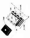
The CP555 Super Integrated Circuit Chip has a ceramic package casing made from (B4-C) Boron Carbide: a non-conducting ceramic material. The IC is connected to connector pins by microcircuits and a custom formulated bond wire. The CP555 Integrated Circuit's ceramic Boron Carbide (B4-C) outer package casing, Heterodiamond substrates and dielectric components allows these integrated circuits to reduce electro-migration to a minimum, produce superior radiation hardness, heat resistance, electromagnetic shielding, and resistance to damage from harsh elements and environments. The CP555 Integrated Circuit can be used as a CMOS, PIC or DIE microcontroller circuit or computer processor (CPU). FIG. 1, shows the integrated circuit package 50, the outer package casing 138 also in FIG. 1, top left. Together, the Heterodiamond (B-C-N) semiconductor substrate and dielectric components, combined with a (Cu—Au—Ag) custom formulated bond wire work synergistically to make The CP555 Super Integrated Circuit Chip a unique semiconductor device.
Assignee:
- Gregory Richard Tarczynski 1 🇺🇸 Chicago, IL, United States
Applicant:
Interested in similar patents?
Get notified when new applications in this technology area are published.
Classification:
H01B1/026 » CPC main
Conductors or conductive bodies characterised by the conductive materials; Selection of materials as conductors mainly consisting of metals or alloys Alloys based on copper
H01L29/1602 » CPC further
Semiconductor devices adapted for rectifying, amplifying, oscillating or switching, or capacitors or resistors with at least one potential-jump barrier or surface barrier, e.g. PN junction depletion layer or carrier concentration layer; Details of semiconductor bodies or of electrodes thereof; Multistep manufacturing processes therefor; Semiconductor bodies ; Multistep manufacturing processes therefor characterised by the materials of which they are formed including, apart from doping materials or other impurities, only elements of Group IV of the Periodic System Diamond
H01L2924/01006 » CPC further
Indexing scheme for arrangements or methods for connecting or disconnecting semiconductor or solid-state bodies as covered by; Chemical elements Carbon [C]
H01L23/495 IPC
Details of semiconductor or other solid state devices; Arrangements for conducting electric current to or from the solid state body in operation, e.g. leads, terminal arrangements ; Selection of materials therefor consisting of soldered constructions Lead-frames or other flat leads
H01B1/02 IPC
Conductors or conductive bodies characterised by the conductive materials; Selection of materials as conductors mainly consisting of metals or alloys
H01L29/16 IPC
Semiconductor devices adapted for rectifying, amplifying, oscillating or switching, or capacitors or resistors with at least one potential-jump barrier or surface barrier, e.g. PN junction depletion layer or carrier concentration layer; Details of semiconductor bodies or of electrodes thereof; Multistep manufacturing processes therefor; Semiconductor bodies ; Multistep manufacturing processes therefor characterised by the materials of which they are formed including, apart from doping materials or other impurities, only elements of Group IV of the Periodic System
H01L23/08 » CPC further
Details of semiconductor or other solid state devices; Containers; Seals characterised by the material of the container or its electrical properties the material being an electrical insulator, e.g. glass
H01L23/00 IPC
Details of semiconductor or other solid state devices
H01L29/26 » CPC further
Semiconductor devices adapted for rectifying, amplifying, oscillating or switching, or capacitors or resistors with at least one potential-jump barrier or surface barrier, e.g. PN junction depletion layer or carrier concentration layer; Details of semiconductor bodies or of electrodes thereof; Multistep manufacturing processes therefor; Semiconductor bodies ; Multistep manufacturing processes therefor characterised by the materials of which they are formed including, apart from doping materials or other impurities, elements provided for in two or more of the groups , , , , , e.g. alloys
H01L2924/01047 » CPC further
Indexing scheme for arrangements or methods for connecting or disconnecting semiconductor or solid-state bodies as covered by; Chemical elements Silver [Ag]
H01L24/45 » CPC further
Arrangements for connecting or disconnecting semiconductor or solid-state bodies; Methods or apparatus related thereto; Means for bonding being attached to, or being formed on, the surface to be connected, e.g. chip-to-package, die-attach, "first-level" interconnects; Manufacturing methods related thereto; Wire connectors; Manufacturing methods related thereto; Structure, shape, material or disposition of the wire connectors prior to the connecting process of an individual wire connector
H01L2924/15787 » CPC further
Indexing scheme for arrangements or methods for connecting or disconnecting semiconductor or solid-state bodies as covered by; Details of package parts other than the semiconductor or other solid state devices to be connected; Die mounting substrate; Material with a principal constituent of the material being a non metallic, non metalloid inorganic material Ceramics, e.g. crystalline carbides, nitrides or oxides
H01L2924/01327 » CPC further
Indexing scheme for arrangements or methods for connecting or disconnecting semiconductor or solid-state bodies as covered by; Alloys; Binary Alloys Intermediate phases, i.e. intermetallics compounds
H01L2924/01015 » CPC further
Indexing scheme for arrangements or methods for connecting or disconnecting semiconductor or solid-state bodies as covered by; Chemical elements Phosphorus [P]
H01L2924/00014 » CPC further
Indexing scheme for arrangements or methods for connecting or disconnecting semiconductor or solid-state bodies as covered by; Technical content checked by a classifier the subject-matter covered by the group, the symbol of which is combined with the symbol of this group, being disclosed without further technical details
Description
BACKGROUND OF INVENTION
The CP555 Super Integrated Circuit Chip semiconductor device is similar to a common Integrated Circuit but, has a superior ceramic outer casing which, is made from Boron Carbide (B4-C) and houses a chip pad and multiple layers of Heterodiamond Substrates with bonding wire that contains: an Au—Cu—Ag alloy including 5-40% Ag by weight in Cu having a purity of 99.999% or greater; at least one element of a first group consisting of Pd, Rh, Pt, and Ir in an amount of about 50-10,000 ppm by weight; at least one element of a second group consisting of B, Be, and Ca in an amount of about 1-50 ppm by weight; at least one element of a third group consisting of P, Sb, and Bi in an amount of about 1-50 ppm by weight; and at least one element of a fourth group consisting of Mg, TI, Zn, and Sn in an amount of about 5-50 ppm by weight. The bonding wire is highly reliable with a strong tensile strength at room temperature and high temperature and favorable bond ability. When the bonding wire is looped, no rupture occurs in a ball neck region. Also, no chip cracking occurs since the ball is soft.
BRIEF DESCRIPTIONS OF DRAWINGS
Referring to FIG. 1, a general semiconductor package includes a semiconductor chip 10 on a pad 50, a plurality of chip pads 20 formed on the semiconductor chip 10 as input/output ports for a variety of signals, a plurality of lead frames 40 electrically connected to the semiconductor chip 10 to receive the variety of signals from or to output the same to an external circuit; and a bonding wire 30 for electrically connecting the chip pad 20 and the lead frame 40. This structure of the general semiconductor package is protected by, for example, the CP555 integrated circuit has a superior ceramic outer casing made from Boron Carbide and houses the chip pad and the Heterodiamond substrate layers. Also, one end of the bonding wire 30 bound to the chip pad 20 includes a compressed ball 32 and a neck 34 as a connector between the compressed ball 32 and the bonding wire 30. In a wire bonding process, one end of the bonding wire 30 is melted by discharging to form a free air ball of a predetermined size and pressed on the chip pad 20 to be bound to the chip pad 20. A loop of the bonding wire 30 having an appropriate height and length is formed to reach a corresponding lead frame 40, and the other end of the bonding wire 30 is bound to the lead frame 40 with an application of pressure. As a result, the semiconductor chip 10 and the lead frame 40 are electrically connected.
A Copper-Silver-Gold (Au—Cu—Ag) alloy is used for the bonding wire 30. Gold and Silver forms a complete solid solution together with Copper, so the alloy can be produced on a large scale, thereby lowering the manufacturing cost of the bonding wire. However, when a loop is formed with the conventional bonding wire 30, the bonding wire 30 often breaks near the neck, as indicated by reference numeral 35. A reduced loop height due to the increasing integration density of a semiconductor device further increases the breakage 35 of the neck 34. The breakage 35 occurs due to a poor tensile strength of the bonding wire 30. Accordingly, a signal transmission path formed by the loop is opened. In addition, the poor strength of the bonding wire 30 Causes a loop sagging or sweeping (indicated by reference numeral 36) in a molding process, so that adjacent loops contact one another. When a bonding wire formed as described above is looped, the loop shape is maintained without sagging due to the strong tensile strength, and the loop sweeping is reduced to lower the probability that a short circuit occurs due to electrical contact with adjacent loops, as described above. The ball shape is also favorable. The bonding wires 130 electrically connect a plurality of chip pads 20 on a semiconductor chip 10 mounted on a pad 20 and a plurality of lead frames 40. After being bound to the chip pad 20, the bonding wire 130 has a compressed ball 132 and a neck 134 connecting the boning wire 130 and the compressed ball 132. According to the present invention, the bonding wire 130 can be smoothly looped without a breakage of the neck 134. The loop shape is favorably maintained without sagging or sweeping. 50 The layers of Heterodiamond Substrate and circuits are the core to entire package which protected by 138 a ceramic Boron Carbide ceramic outer casing.
DETAILED DESCRIPTION OF INVENTION
This structure of this semiconductor package is protected by, the CP555 integrated circuit, a superior ceramic outer casing made from Boron Carbide and houses the chip pad and the Heterodiamond substrate layers. The general purpose for this came about because, of the current dilemma that occurs with CMOS Scaling and electromigration beyond 8 nm. As described above, the Cu—Au—Ag alloy bonding wire according to the present invention has a lot of synergy between the added elements. Also, the free air ball is softer than conventional one, so chip cracking nearly does not occur during a wire bonding process. Even when an ultra-low loop is formed with the bonding wire according to the present invention, almost no breakage occurs near the neck.
According to the present invention, ball grain refinements are suppressed to reduce the grain area, thereby reducing an atomic diffusion path between Au and Ag. Accordingly, intermetallic compound and Kirkendall void formation is suppressed, thereby improving thermal stability. The bonding wire according to the present invention has a strong tensile strength at room temperature and high temperature, and the loop shape after bonding is constantly maintained. In addition, the adhesion between the bonding wire and the chip pad is excellent and is maintained even after a high-temperature process for a long period of time. The ceramic outer casing made from Boron Carbide and its thermal resistance and protection from harsh elements and environments, the unique semiconductor qualities of the Heterodiamond substrate layers and the bonding wire according and to the present invention are favorable, and thus according to the present invention have wide industrial applications and numerous applications in many other fields, the forming of a new electrical interconnection in semiconductor packages. The present invention has been particularly shown and described with reference to preferred embodiments thereof. It will be understood by those of ordinary skill in the art that various changes in form and details may be made therein without departing from the spirit and scope of the present invention as defined by the appended claims.
Claims
What is claimed is:1. This type of semiconductor device consist of a ceramic package containing B4-C Boron carbide, a ceramic material which is obtained by decomposing B2O3 with carbon in an electric furnace, it's unique and exceptional qualities produce superior radiation hardness, heat resistance, electromagnetic shielding, and resistance to damage from harsh elements and environments.
2. Heterodiamond, symbol B-C-N, is used as a substrate material in this type of integrated circuit, this semiconductor substrate, because of Heterodiamond's unique semiconductor electrical behavior, between that of a conductor and an insulator at room temperature; with the proper addition of dopant element (silicon and Gallium), p-n junctions can be formed on Heterodiamond and can be useful to electronic components and integrated circuits that are built from p-n junctions; Heterodiamond is a super-hard compound of boron, carbon, and nitrogen.
3. A bonding wire for this type of semiconductor device, containing: a Cu—Au—Ag alloy including 5-20% Ag and 5-20% Au—by weight in Cu having a purity of 99.999% or greater, also at least one element of a first group consisting of Pd, Rh, Pt, and Jr in an amount of about 50-10,000 ppm by weight; at least one element of a second group consisting of B, Be, and Ca in an amount of about 1-50 ppm by weight; at least one element of a third group consisting of P, Sb, and Bi in an amount of about 1-50 ppm by weight; and at least one element of a fourth group consisting of Mg, TI, Zn, and Sn in an amount of about 5-50 ppm by weight.
4. The bonding wire of claim 3, wherein as many kinds of elements as possible from each of the first through fourth groups are added for synergism.
5. The bonding wire of claim 3, essentially containing 15-30% Ag and Au by weight, Pd, Be, Ca, and Mg.
6. The bonding wire of claim 3, containing: 15-30% Ag and Au by weight, Pd and Pt each in an amount of about 500-1,500 ppm by weight; B, Be, and Ca each in an amount of about 1-30 ppm by weight; P, Sb, and Bi each in an amount of about 3-30 ppm by weight; and Mg and Zn each in an amount of 3-30 ppm by weight.
7. The bonding wire of claim 3, containing: 10-30% Ag and Au by weight; Pd in an amount of about 1,000-10,000 ppm by weight; Be and Ca each in an amount of about 5-20 ppm by weight; P and Bi each in an amount of about 5-20 ppm by weight; and Mg, Zn, and Sn each in an amount of about 5-20 ppm by weight.
8. The bonding wire of claim 3, containing: 10-30% Ag and Au by weight; Pd, Rh, Pt, and Ir each in an amount of about 100-10,000 ppm by weight; Be and Ca each in an amount of about 5-30 ppm by weight; Sb and Bi each in an amount of about 5-20 ppm by weight; and Mg and Sn each in an amount of about 5-30 ppm by weight.
9. The bonding wire of claim 3, containing: 10-30% Ag and Au by weight; Pd, Rh, and Pt each in an amount of about 100-10,000 ppm by weight; B, Be, and Ca each in an amount of about 2-30 ppm by weight; P and Bi each in an amount of about 5-20 ppm by weight; and Mg, TI, Zn, and Sn each in an amount of about 3-30 ppm by weight.
10. The bonding wire of claim 3, containing: 10-30% Ag and Au by weight; Pd and Pt each in an amount of about 500-10,000 ppm by weight; B, Be, and Ca each in an amount of about 2-30 ppm by weight; Sb and Bi each in an amount of about 5-20 ppm by weight; and Mg, TI, and Zn each in an amount of about 3-20 ppm by weight.
Images & Drawings included:

Sources:
- United States Patent and Trademark Office - verify current appl. status at the USPTO↗
Recent applications in this class:
- » 20250273360 2025-08-28
CARBON-NANOTUBES COPPER COMPOSITE CONDUCTORS - » 20250218619 2025-07-03
GROUND CONDUCTOR - » 20250022628 2025-01-16
COPPER ALLOY WIRE, COVERED WIRE, COVERED WIRE WITH TERMINAL, AND METHOD FOR MANUFACTURING COPPER ALLOY WIRE - » 20250006400 2025-01-02
POWER TOOLS WITH A CURRENT CONDUCTOR, AND ENERGY SUPPLY DEVICE - » 20250006399 2025-01-02
SYSTEM COMPRISING A POWER TOOL AND AN ENERGY SUPPLY DEVICE, AND ENERGY SUPPLY DEVICE - » 20240395438 2024-11-28
CONDUCTIVE CABLE FOR A BATTERY ELECTRIC VEHICLE - » 20240339238 2024-10-10
CU-AG ALLOY WIRE AND METHOD FOR PRODUCING THE SAME - » 20240331891 2024-10-03
Conductive wire for electrical properties testing and method for producing the same - » 20240177883 2024-05-30
TRANSPARENT CONDUCTIVE FILM, METHOD FOR PRODUCING TRANSPARENT CONDUCTIVE FILM, TRANSPARENT CONDUCTIVE MEMBER, ELECTRONIC DISPLAY DEVICE, AND SOLAR BATTERY - » 20240029914 2024-01-25
ELECTRICALLY CONDUCTIVE WIRE