Method and device for electrically contacting terminal faces of two substrates by laser soldering using a gaseous flux medium
US20140027418A1
2014-01-30
13/982,837
2012-01-30
✅ Patent granted
US 9,649,711 B2
2017-05-16
WO; PCT/DE2012/000068; 20120130
WO; WO2012/103868; 20120809
Geoffrey S Evans
Quarles & Brady LLP
2033-12-21
Abstract:
The present invention relates to a method for electrically contacting terminal faces of two substrates (6, 7), in particular of a chip (6) and of a carrier substrate (7). Furthermore, the invention relates to a device for performing a second phase of the method according to the invention. The method according to the invention takes place in two successive phases, wherein, in a first phase, the chip (6) is positioned with its terminal faces against terminal faces of the substrate (7) and laser energy (5) is applied to the chip (6) at the rear and, in a subsequent second phase, in a housing (3), a flux medium is applied and at the same time a reflow is performed by means of laser energy (5) being applied to the chip (6) at the rear, and a process of rinsing the housing interior is subsequently performed. The device according to the invention for performing a second phase of the method comprises a carrier table (1) and a housing (3), which together with a top side of the carrier table (1) forms a housing interior, in which the component arrangement is positioned, and also a laser light source (5), which is oriented in such a way that the laser radiation impinges on the first substrate (6) on the rear side.
Assignee:
- Pac Tech- Packaging Technologies GmbH 41 🇩🇪 Nauen, Germany
Applicant:
Interested in similar patents?
Get notified when new applications in this technology area are published.
Classification:
B23K1/0056 » CPC main
Soldering, e.g. brazing, or unsoldering; Soldering by means of radiant energy soldering by means of beams, e.g. lasers, E.B.
B23K35/362 » CPC further
Rods, electrodes, materials, or media, for use in soldering, welding, or cutting characterised by the composition or nature of the material; Selection of non-metallic compositions, e.g. coatings, fluxes ; Selection of soldering or welding materials, conjoint with selection of non-metallic compositions, both selections being of interest Selection of compositions of fluxes
B23K1/005 IPC
Soldering, e.g. brazing, or unsoldering Soldering by means of radiant energy
B23K26/02 » CPC further
Working by laser beam, e.g. welding, cutting or boring Positioning or observing the workpiece, e.g. with respect to the point of impact; Aligning, aiming or focusing the laser beam
H01L24/75 » CPC further
Arrangements for connecting or disconnecting semiconductor or solid-state bodies; Methods or apparatus related thereto; Apparatus for manufacturing arrangements for connecting or disconnecting semiconductor or solid-state bodies Apparatus for connecting with bump connectors or layer connectors
H01L24/16 » CPC further
Arrangements for connecting or disconnecting semiconductor or solid-state bodies; Methods or apparatus related thereto; Means for bonding being attached to, or being formed on, the surface to be connected, e.g. chip-to-package, die-attach, "first-level" interconnects; Manufacturing methods related thereto; Bump connectors ; Manufacturing methods related thereto; Structure, shape, material or disposition of the bump connectors after the connecting process of an individual bump connector
H01L24/94 » CPC further
Arrangements for connecting or disconnecting semiconductor or solid-state bodies; Methods or apparatus related thereto; Batch processes at wafer-level, i.e. with connecting carried out on a wafer comprising a plurality of undiced individual devices
H01L25/0657 » CPC further
Assemblies consisting of a plurality of individual semiconductor or other solid state devices ; Multistep manufacturing processes thereof all the devices being of a type provided for in the same subgroup of groups - , e.g. assemblies of rectifier diodes the devices not having separate containers the devices being of a type provided for in group Stacked arrangements of devices
H01L25/50 » CPC further
Assemblies consisting of a plurality of individual semiconductor or other solid state devices ; Multistep manufacturing processes thereof Multistep manufacturing processes of assemblies consisting of devices, each device being of a type provided for in group or
H01L2224/7501 » CPC further
Indexing scheme for arrangements for connecting or disconnecting semiconductor or solid-state bodies and methods related thereto as covered by; Apparatus for manufacturing arrangements for connecting or disconnecting semiconductor or solid-state bodies and for methods related thereto; Apparatus for connecting with bump connectors or layer connectors Means for cleaning, e.g. brushes, for hydro blasting, for ultrasonic cleaning, for dry ice blasting, using gas-flow, by etching, by applying flux or plasma
H01L2224/75101 » CPC further
Indexing scheme for arrangements for connecting or disconnecting semiconductor or solid-state bodies and methods related thereto as covered by; Apparatus for manufacturing arrangements for connecting or disconnecting semiconductor or solid-state bodies and for methods related thereto; Apparatus for connecting with bump connectors or layer connectors; Means for controlling the bonding environment, e.g. valves, vacuum pumps Chamber
H01L2224/75263 » CPC further
Indexing scheme for arrangements for connecting or disconnecting semiconductor or solid-state bodies and methods related thereto as covered by; Apparatus for manufacturing arrangements for connecting or disconnecting semiconductor or solid-state bodies and for methods related thereto; Apparatus for connecting with bump connectors or layer connectors; Means for applying energy, e.g. heating means; Laser in the upper part of the bonding apparatus, e.g. in the bonding head
H01L2224/81065 » CPC further
Indexing scheme for arrangements for connecting or disconnecting semiconductor or solid-state bodies and methods related thereto as covered by; Methods for connecting semiconductor or other solid state bodies using means for bonding being attached to, or being formed on, the surface to be connected using a bump connector; Bonding environment; Composition of the atmosphere being reducing
H01L2224/8191 » CPC further
Indexing scheme for arrangements for connecting or disconnecting semiconductor or solid-state bodies and methods related thereto as covered by; Methods for connecting semiconductor or other solid state bodies using means for bonding being attached to, or being formed on, the surface to be connected using a bump connector; Post-treatment of the bump connector or bonding area Cleaning, e.g. oxide removal step, desmearing
H01L2224/81191 » CPC further
Indexing scheme for arrangements for connecting or disconnecting semiconductor or solid-state bodies and methods related thereto as covered by; Methods for connecting semiconductor or other solid state bodies using means for bonding being attached to, or being formed on, the surface to be connected using a bump connector; Arrangement of the bump connectors prior to mounting wherein the bump connectors are disposed only on the semiconductor or solid-state body
H01L2224/81192 » CPC further
Indexing scheme for arrangements for connecting or disconnecting semiconductor or solid-state bodies and methods related thereto as covered by; Methods for connecting semiconductor or other solid state bodies using means for bonding being attached to, or being formed on, the surface to be connected using a bump connector; Arrangement of the bump connectors prior to mounting wherein the bump connectors are disposed only on another item or body to be connected to the semiconductor or solid-state body
H01L2224/81224 » CPC further
Indexing scheme for arrangements for connecting or disconnecting semiconductor or solid-state bodies and methods related thereto as covered by; Methods for connecting semiconductor or other solid state bodies using means for bonding being attached to, or being formed on, the surface to be connected using a bump connector; Applying energy for connecting with energy being in the form of electromagnetic radiation using a laser
H01L2224/81815 » CPC further
Indexing scheme for arrangements for connecting or disconnecting semiconductor or solid-state bodies and methods related thereto as covered by; Methods for connecting semiconductor or other solid state bodies using means for bonding being attached to, or being formed on, the surface to be connected using a bump connector; Bonding techniques; Soldering or alloying Reflow soldering
H01L2224/81907 » CPC further
Indexing scheme for arrangements for connecting or disconnecting semiconductor or solid-state bodies and methods related thereto as covered by; Methods for connecting semiconductor or other solid state bodies using means for bonding being attached to, or being formed on, the surface to be connected using a bump connector; Combinations of bonding methods provided for in at least two different groups from - Intermediate bonding, i.e. intermediate bonding step for temporarily bonding the semiconductor or solid-state body, followed by at least a further bonding step
H01L2224/81986 » CPC further
Indexing scheme for arrangements for connecting or disconnecting semiconductor or solid-state bodies and methods related thereto as covered by; Methods for connecting semiconductor or other solid state bodies using means for bonding being attached to, or being formed on, the surface to be connected using a bump connector Specific sequence of steps, e.g. repetition of manufacturing steps, time sequence
H01L2225/06513 » CPC further
Details relating to assemblies covered by the group but not provided for in its subgroups; All the devices being of a type provided for in the same subgroup of groups - the devices not having separate containers the devices being of a type provided for in group; Stacked arrangements of devices Bump or bump-like direct electrical connections between devices, e.g. flip-chip connection, solder bumps
H01L2225/06517 » CPC further
Details relating to assemblies covered by the group but not provided for in its subgroups; All the devices being of a type provided for in the same subgroup of groups - the devices not having separate containers the devices being of a type provided for in group; Stacked arrangements of devices Bump or bump-like direct electrical connections from device to substrate
H01L2924/014 » CPC further
Indexing scheme for arrangements or methods for connecting or disconnecting semiconductor or solid-state bodies as covered by; Alloys Solder alloys
H01L23/00 IPC
Details of semiconductor or other solid state devices
H01L25/065 IPC
Assemblies consisting of a plurality of individual semiconductor or other solid state devices ; Multistep manufacturing processes thereof all the devices being of a type provided for in the same subgroup of groups - , e.g. assemblies of rectifier diodes the devices not having separate containers the devices being of a type provided for in group
H01L25/00 IPC
Assemblies consisting of a plurality of individual semiconductor or other solid state devices ; Multistep manufacturing processes thereof
H01L2924/12042 » CPC further
Indexing scheme for arrangements or methods for connecting or disconnecting semiconductor or solid-state bodies as covered by; Details of semiconductor or other solid state devices to be connected; Device type; Passive devices, e.g. 2 terminal devices; Optical Diode LASER
H01L24/81 » CPC further
Arrangements for connecting or disconnecting semiconductor or solid-state bodies; Methods or apparatus related thereto; Methods for connecting semiconductor or other solid state bodies using means for bonding being attached to, or being formed on, the surface to be connected using a bump connector
H01L2224/81193 » CPC further
Indexing scheme for arrangements for connecting or disconnecting semiconductor or solid-state bodies and methods related thereto as covered by; Methods for connecting semiconductor or other solid state bodies using means for bonding being attached to, or being formed on, the surface to be connected using a bump connector; Arrangement of the bump connectors prior to mounting wherein the bump connectors are disposed on both the semiconductor or solid-state body and another item or body to be connected to the semiconductor or solid-state body
Description
The present invention relates to a method for electrically contacting terminal faces of two substrates, wherein the first substrate with its terminal faces facing the second substrate is electrically and mechanically connected directly to the terminal faces of the second substrate and the terminal faces of the first substrate are provided with a soldering agent coating. For forming a chip module, in particular, the first substrate can be a chip and the second substrate can be a carrier substrate, wherein the chip is contacted face down with its chip terminal faces against the substrate terminal faces.
Furthermore, the invention relates to a device for performing a second phase of the method according to the invention.
From the generic state of the art, methods for the direct mounting of semiconductor chips on carrier substrates are known. There are, for example, methods in which the unpackaged chip is fixed directly on the carrier substrate or on a printed circuit board with its terminal faces facing the carrier substrate and with soldering agents (solder balls) previously applied to the terminal faces of the chip. For this purpose, the soldering agent coating is re-melted during reflow soldering in a soldering furnace and forms a connection with the terminal faces of the carrier substrate. Methods of this type are highly complex in terms of their process flow as well as regarding the required apparatuses.
Therefore, it is the object of the present invention to propose a method and a device for the implementation thereof which technically simplify the process of electrically contacting terminal faces of two substrates, in particular of semiconductor components with carrier substrates, and thus to improve economic efficiency.
The method according to the invention takes place in two successive phases, wherein, in phase I, the chip is positioned with its terminal faces against the terminal faces of the substrate, and the chip terminal faces and/or the substrate terminal faces are provided with a soldering agent coating. In phase I, laser energy is applied to the chip at the rear in such a manner that the soldering agent is melted or partially melted at least to such an extent so as to enable a fixation of the chip on the substrate, wherein, simultaneously, a leveling or a uniform flattening of the soldering agent coatings provided on the chip terminal faces or on the substrate terminal faces takes place so that a contact is formed between all chip terminal faces and substrate terminal faces.
Following phase I, the component arrangement formed by the chip and the substrate is disposed in a housing, which is realized in such a manner that during a reflow of the solder material coating, a flux medium is applied to the component arrangement, the flux medium being in particular gaseous and preferably consisting of a mixture of nitrogen and formic acid. It is particularly advantageous if the housing is formed such that a flowing of the medium through the housing interior takes place, wherein, simultaneously with the application, a reflow takes place due to the application of laser energy to the chip at the rear, similarly to the previously described phase I.
Following the application of the flux medium, which enables in particular a breaking of an oxide layer which may have formed on the soldering agent coating in phase I, a process of rinsing the housing interior takes place, for which exclusively a protective gas is preferably utilized.
Further advantageous implementation features result from the following description and the drawing, which illustrates a preferred embodiment of the invention using an example.
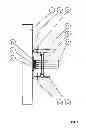
FIG. 1 shows a schematic illustration of the device according to the invention.
In FIG. 1, a device for implementing the method is illustrated during phase II after the afore-described fixation of the chip on the substrate has taken place in phase I, which is not illustrated here. Once phase I has been completed, the component arrangement is brought into the position illustrated in FIG. 1, in which position it is located below the housing 3, and then the housing 3 is lowered onto the component arrangement as illustrated in FIG. 1.
In phase II, the component arrangement formed by the chip 6 and the substrate 7 is located in the interior of a housing 3, which is sealed against the outside by a seal 2 closing with the carrier table 1. In a wall otherwise substantially gas-tight against the environment, the housing 3 has an inlet opening 8 and an outlet opening 9, which enable a flow-through, respectively a rinsing or flooding of the housing interior with a gaseous medium. The housing wall, which is arranged substantially parallel to a rear side of the chip 6, is formed by a glass plate or a transparent plate, which enables an application of laser energy 5 to the chip at the rear, the laser radiation being focused corresponding to the dimensions of the rear side of the chip 6 so as to avoid a direct introduction of heat or energy into the substrate 7. The application of laser energy 5 to the chip 6 at the rear causes a reflow of the soldering agent coating 10 arranged between the chip terminal faces and the substrate terminal faces while a flux medium is flowing through the housing interior, the flux medium in the present case being formed by a mixture of nitrogen and formic acid. For forming said gas mixture, for example, a nitrogen flow can be guided over the surface of a formic acid bath outside of the housing 3 so that the vapor of the formic acid, which is carried along, blends with the nitrogen before flowing into the housing 3. After the reflow has taken place, meaning in particular after laser energy has been applied to the rear side of the chip, a preferably pure protective gas flow flows through or rinses the interior of the housing 3, a nitrogen flow being preferably used here, so as to avoid flux medium depositions, meaning in particular depositions of formic acid, on the component arrangement 6/7.
Instead of the formic acid mentioned as an example here, any gaseous flux medium which has comparable effects can basically be used.
In deviation from the illustration of the component arrangement exemplarily illustrated in FIG. 1 as a combination of a chip 6 and a substrate 7, it is also possible to implement the method according to the invention on a wafer level, i.e. for connecting two wafers.
Furthermore, in deviation from the chosen illustration, it is also possible to not only connect a chip and a substrate or to melt soldering agent coatings or deposits arranged between the substrate terminal faces and the chip terminal faces in a reflow process, but also to connect stacked arrangements of chips, comprising a plurality of chips arranged one on top of the other, to a substrate.
Claims
1. A method for electrically contacting terminal faces of two substrates, said method comprising:
providing a first substrate with terminal faces facing a second substrate, wherein the terminal faces of the first substrate are provided with a soldering agent
positioning the terminal faces of the first substrate against terminal faces of the second substrate;
applying laser energy to a rear of the first substrate in such a manner that the soldering agent is melted at least to such an extent so as to enable a mechanical fixation of the first substrate on the second substrate and an electrical contacting of the terminal faces facing each other;
applying a flux medium, in a housing interior, to a component arrangement formed by the first and second substrates;
simultaneously with the step of applying the flux medium, re-melting soldering agent using laser energy applied to the rear of the first substrate; and
subsequently rinsing the housing interior.
2. The method according to claim 1, in which the flux medium is in a gaseous state.
3. The method according to claim 2, in which the gaseous flux medium consists of a mixture of nitrogen and formic acid.
4. The method according to claim 3, in which for forming the gaseous flux medium, outside of the housing interior, a nitrogen flow is guided over a surface of a formic acid bath so that the vapors of the formic acid, which are carried along, blend with the nitrogen before being applied to the component arrangement.
5. The method according to claim 1, in which the rinsing is performed with a pure protective gas flow.
6. The method according to claim 5, in which the pure protective gas flow is a nitrogen flow.
7. A device for carrying out a portion of the method according to claim 1, said device comprising:
a carrier table supporting a component arrangement formed by the first and second substrates;
a housing enclosing the component arrangement and together with a top side of the carrier table forming the housing interior; and
a laser light source oriented such that laser radiation impinges on the rear side of the first substrate.
8. The device according to claim 7, in which the housing is provided with a circumferential seal closing with the top side of the carrier table.
9. The device according to claim 7, in which the housing has an inlet opening and an outlet opening, which enable a flux medium or a rinsing medium to flow through the housing interior.
10. The device according to claim 7, in which, a housing wall of the housing, which is arranged substantially parallel to the rear of the first substrate, is formed as a transparent plate to enable application of laser energy to the rear of the first substrate.
Images & Drawings included:

Sources:
- United States Patent and Trademark Office - verify current appl. status at the USPTO↗
Recent applications in this class:
- » 20250276393 2025-09-04
BONDING METHOD AND LASER PROCESSING APPARATUS - » 20250196244 2025-06-19
METHOD AND LASER ARRANGEMENT FOR ELECTRICALLY CONTACTING TERMINAL FACES OF TWO SUBSTRATES - » 20250135568 2025-05-01
DEVICE FOR TRANSFERRING AND METHOD - » 20250033130 2025-01-30
LASER SOLDERING DEVICE WITH ADJUSTABLE LASER IRRADIATION POSITION AND SOLDERING METHOD COMPRISING SAME - » 20250001511 2025-01-02
ELECTRON BEAM BRAZING TO REPAIR COMPONENT - » 20240408687 2024-12-12
SOLDER SOLDERING METHOD USING LASER - » 20240408686 2024-12-12
METHOD FOR BRAZE FILLER METAL PREPARATION - » 20240253142 2024-08-01
LASER SOLDERING APPARATUS, CONTROL APPARATUS, AND LASER SOLDERING METHOD - » 20240123531 2024-04-18
LASER BRAZING METHOD - » 20240109144 2024-04-04
Laser-Assisted Soldering Apparatus
Recent applications for this Assignee:
- » 20240373563 2024-11-07
Method for Soldering an Electronic Component to a Circuit Board by Jetting Liquefied Solder into a Through Hole - » 20240359272 2024-10-31
Bonding Head and Bonding Apparatus - » 20220369473 2022-11-17
Method for soldering an electronic component to a circuit board by jetting liquefied solder into a through hole - » 20220132714 2022-04-28
Method for removing and repositioning electronic components connected to a circuit board - » 20220126398 2022-04-28
Method for removing electronic components connected to a circuit board - » 20210299800 2021-09-30
Method and device including laser heating of gripper for repairing a test contact arrangement - » 20210220934 2021-07-22
Method and laser arrangement for fusing a solder material deposit by means of laser energy - » 20210193619 2021-06-24
Semiconductor chip stack arrangement and semiconductor chip for producing such a semiconductor chip stack arrangement - » 20200269336 2020-08-27
Solder ball feeding device - » 20200161273 2020-05-21
Method and device for establishing a wire connection as well as a component arrangement having a wire connection