Method for electrically connecting wafers using butting contact structure and semiconductor device fabricated through the same
US20140138847A1
2014-05-22
14/079,075
2013-11-13
✅ Patent granted
US 8,906,781 B2
2014-12-09
-
-
Bradley K Smith
Kile Park Reed & Houtteman PLLC
2033-11-13
Abstract:
The present invention relates to a method for electrically connecting wafers, which physically bonds two wafers through an oxide-to-oxide bonding method and then electrically connects the two wafers through a butting contact structure. The wafers are physically bonded to each other through a relatively simple method, and then electrically connected to through TSVs or butting contact holes. Therefore, since the fabrication process may be simplified, a process error may be reduced, and the product yield may be improved.
Assignee:
- SILICONFILE TECHNOLOGIES INC. 1 🇰🇷 Seongnam-si, South Korea
- SiliconFile Technologies Inc. 4 🇰🇷 Seongnam-si, Gyeonggi-do, South Korea
Applicant:
Interested in similar patents?
Get notified when new applications in this technology area are published.
Classification:
H01L25/50 » CPC main
Assemblies consisting of a plurality of individual semiconductor or other solid state devices ; Multistep manufacturing processes thereof Multistep manufacturing processes of assemblies consisting of devices, each device being of a type provided for in group or
H01L21/76802 » CPC further
Processes or apparatus adapted for the manufacture or treatment of semiconductor or solid state devices or of parts thereof; Manufacture or treatment of devices consisting of a plurality of solid state components formed in or on a common substrate or of parts thereof; Manufacture of integrated circuit devices or of parts thereof; Manufacture of specific parts of devices defined in group; Applying interconnections to be used for carrying current between separate components within a device comprising conductors and dielectrics characterised by the formation and the after-treatment of the dielectrics, e.g. smoothing by forming openings in dielectrics
H01L27/14634 » CPC further
Devices consisting of a plurality of semiconductor or other solid-state components formed in or on a common substrate including semiconductor components sensitive to infra-red radiation, light, electromagnetic radiation of shorter wavelength or corpuscular radiation and specially adapted either for the conversion of the energy of such radiation into electrical energy or for the control of electrical energy by such radiation; Devices controlled by radiation; Imager structures; Structural or functional details thereof Assemblies, i.e. Hybrid structures
H01L2224/9212 » CPC further
Indexing scheme for arrangements for connecting or disconnecting semiconductor or solid-state bodies and methods related thereto as covered by; Methods for connecting semiconductor or solid state bodies including different methods provided for in two or more of groups - ; Specific sequence of method steps; Connecting a surface with connectors of different types Sequential connecting processes
H01L23/481 » CPC further
Details of semiconductor or other solid state devices; Arrangements for conducting electric current to or from the solid state body in operation, e.g. leads, terminal arrangements ; Selection of materials therefor Internal lead connections, e.g. via connections, feedthrough structures
H01L24/80 » CPC further
Arrangements for connecting or disconnecting semiconductor or solid-state bodies; Methods or apparatus related thereto Methods for connecting semiconductor or other solid state bodies using means for bonding being attached to, or being formed on, the surface to be connected
H01L24/92 » CPC further
Arrangements for connecting or disconnecting semiconductor or solid-state bodies; Methods or apparatus related thereto; Methods for connecting semiconductor or solid state bodies including different methods provided for in two or more of groups - Specific sequence of method steps
H01L27/1469 » CPC further
Devices consisting of a plurality of semiconductor or other solid-state components formed in or on a common substrate including semiconductor components sensitive to infra-red radiation, light, electromagnetic radiation of shorter wavelength or corpuscular radiation and specially adapted either for the conversion of the energy of such radiation into electrical energy or for the control of electrical energy by such radiation; Devices controlled by radiation; Imager structures; Processes or apparatus peculiar to the manufacture or treatment of these devices or parts thereof Assemblies, i.e. hybrid integration
H01L2224/821 » CPC further
Indexing scheme for arrangements for connecting or disconnecting semiconductor or solid-state bodies and methods related thereto as covered by; Methods for connecting semiconductor or other solid state bodies using means for bonding being attached to, or being formed on, the surface to be connected by forming build-up interconnects at chip-level, e.g. for high density interconnects [HDI] Forming a build-up interconnect
H01L24/06 » CPC further
Arrangements for connecting or disconnecting semiconductor or solid-state bodies; Methods or apparatus related thereto; Means for bonding being attached to, or being formed on, the surface to be connected, e.g. chip-to-package, die-attach, "first-level" interconnects; Manufacturing methods related thereto; Bonding areas ; Manufacturing methods related thereto; Structure, shape, material or disposition of the bonding areas prior to the connecting process of a plurality of bonding areas
H01L24/08 » CPC further
Arrangements for connecting or disconnecting semiconductor or solid-state bodies; Methods or apparatus related thereto; Means for bonding being attached to, or being formed on, the surface to be connected, e.g. chip-to-package, die-attach, "first-level" interconnects; Manufacturing methods related thereto; Bonding areas ; Manufacturing methods related thereto; Structure, shape, material or disposition of the bonding areas after the connecting process of an individual bonding area
H01L24/82 » CPC further
Arrangements for connecting or disconnecting semiconductor or solid-state bodies; Methods or apparatus related thereto; Methods for connecting semiconductor or other solid state bodies using means for bonding being attached to, or being formed on, the surface to be connected by forming build-up interconnects at chip-level, e.g. for high density interconnects [HDI]
H01L2224/05573 » CPC further
Indexing scheme for arrangements for connecting or disconnecting semiconductor or solid-state bodies and methods related thereto as covered by; Means for bonding being attached to, or being formed on, the surface to be connected, e.g. chip-to-package, die-attach, "first-level" interconnects; Manufacturing methods related thereto; Bonding areas; Manufacturing methods related thereto; Structure, shape, material or disposition of the bonding areas prior to the connecting process of an individual bonding area; External layer Single external layer
H01L2224/06051 » CPC further
Indexing scheme for arrangements for connecting or disconnecting semiconductor or solid-state bodies and methods related thereto as covered by; Means for bonding being attached to, or being formed on, the surface to be connected, e.g. chip-to-package, die-attach, "first-level" interconnects; Manufacturing methods related thereto; Bonding areas; Manufacturing methods related thereto; Structure, shape, material or disposition of the bonding areas prior to the connecting process of a plurality of bonding areas; Shape Bonding areas having different shapes
H01L2224/06505 » CPC further
Indexing scheme for arrangements for connecting or disconnecting semiconductor or solid-state bodies and methods related thereto as covered by; Means for bonding being attached to, or being formed on, the surface to be connected, e.g. chip-to-package, die-attach, "first-level" interconnects; Manufacturing methods related thereto; Bonding areas; Manufacturing methods related thereto; Structure, shape, material or disposition of the bonding areas prior to the connecting process of a plurality of bonding areas; Material Bonding areas having different materials
H01L2224/80895 » CPC further
Indexing scheme for arrangements for connecting or disconnecting semiconductor or solid-state bodies and methods related thereto as covered by; Methods for connecting semiconductor or other solid state bodies using means for bonding being attached to, or being formed on, the surface to be connected by connecting a bonding area directly to another bonding area, i.e. connectorless bonding, e.g. bumpless bonding; Bonding techniques; Direct bonding, i.e. joining surfaces by means of intermolecular attracting interactions at their interfaces, e.g. covalent bonds, van der Waals forces between electrically conductive surfaces, e.g. copper-copper direct bonding, surface activated bonding
H01L2224/80896 » CPC further
Indexing scheme for arrangements for connecting or disconnecting semiconductor or solid-state bodies and methods related thereto as covered by; Methods for connecting semiconductor or other solid state bodies using means for bonding being attached to, or being formed on, the surface to be connected by connecting a bonding area directly to another bonding area, i.e. connectorless bonding, e.g. bumpless bonding; Bonding techniques; Direct bonding, i.e. joining surfaces by means of intermolecular attracting interactions at their interfaces, e.g. covalent bonds, van der Waals forces between electrically insulating surfaces, e.g. oxide or nitride layers
H01L2224/9202 » CPC further
Indexing scheme for arrangements for connecting or disconnecting semiconductor or solid-state bodies and methods related thereto as covered by; Methods for connecting semiconductor or solid state bodies including different methods provided for in two or more of groups - ; Specific sequence of method steps Forming additional connectors after the connecting process
H01L24/07 » CPC further
Arrangements for connecting or disconnecting semiconductor or solid-state bodies; Methods or apparatus related thereto; Means for bonding being attached to, or being formed on, the surface to be connected, e.g. chip-to-package, die-attach, "first-level" interconnects; Manufacturing methods related thereto; Bonding areas ; Manufacturing methods related thereto Structure, shape, material or disposition of the bonding areas after the connecting process
H01L2224/82031 » CPC further
Indexing scheme for arrangements for connecting or disconnecting semiconductor or solid-state bodies and methods related thereto as covered by; Methods for connecting semiconductor or other solid state bodies using means for bonding being attached to, or being formed on, the surface to be connected by forming build-up interconnects at chip-level, e.g. for high density interconnects [HDI]; Pre-treatment of the connector or the bonding area; Reshaping, e.g. forming vias by chemical means, e.g. etching, anodisation
H01L21/46 IPC
Processes or apparatus adapted for the manufacture or treatment of semiconductor or solid state devices or of parts thereof; Manufacture or treatment of semiconductor devices or of parts thereof the devices having at least one potential-jump barrier or surface barrier, e.g. PN junction, depletion layer or carrier concentration layer the devices having semiconductor bodies not provided for in groups, , , and with or without impurities, e.g. doping materials Treatment of semiconductor bodies using processes or apparatus not provided for in groups
H01L25/00 IPC
Assemblies consisting of a plurality of individual semiconductor or other solid state devices ; Multistep manufacturing processes thereof
H01L23/48 IPC
Details of semiconductor or other solid state devices Arrangements for conducting electric current to or from the solid state body in operation, e.g. leads, terminal arrangements ; Selection of materials therefor
H01L23/00 IPC
Details of semiconductor or other solid state devices
H01L21/768 IPC
Processes or apparatus adapted for the manufacture or treatment of semiconductor or solid state devices or of parts thereof; Manufacture or treatment of devices consisting of a plurality of solid state components formed in or on a common substrate or of parts thereof; Manufacture of integrated circuit devices or of parts thereof; Manufacture of specific parts of devices defined in group Applying interconnections to be used for carrying current between separate components within a device comprising conductors and dielectrics
H01L27/146 IPC
Devices consisting of a plurality of semiconductor or other solid-state components formed in or on a common substrate including semiconductor components sensitive to infra-red radiation, light, electromagnetic radiation of shorter wavelength or corpuscular radiation and specially adapted either for the conversion of the energy of such radiation into electrical energy or for the control of electrical energy by such radiation; Devices controlled by radiation Imager structures
Description
BACKGROUND OF THE INVENTION
1. Field of the Invention
The present invention relates to a method for electrically connecting two wafers, and more particularly, to a method for electrically connecting wafers using a butting contact structure, which physically bonds two wafers according to an oxide-to-oxide bonding method and then electrically connects the two wafers using a butting contact structure.
2. Description of the Related Art
Recently, the process for reducing the physical size of an integrated circuit by reducing the sizes of devices on a wafer has reached the limit. In order to overcome such a limit, a method of vertically stacking two or more wafers has been proposed.
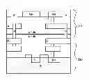
FIG. 1 is a cross-sectional view of a conventional semiconductor device fabricated through a metal-to-metal bonding method.
For convenience of description, suppose that the semiconductor device of FIG. 1 is a part of an image sensor. The semiconductor device includes an upper wafer 110 and a lower wafer 120. The upper wafer 110 includes a photodiode PD to generate charges corresponding to the amount of light incident from the top and a floating diffusion FD to temporarily store the charges. The lower wafer 120 includes elements constituting the image sensor excluding the photodiode PD.
Referring to FIG. 1, two wafers each having different elements implemented therein are bonded to each other. In FIG. 1, A, B, D, and D represents regions in which a metal as a conductive material or polycrystalline silicon is formed. The regions A and C formed in the upper wafer 110 must be electrically connected to the regions B and D formed in the lower wafer 120, respectively.
When a semiconductor fabrication process is completed, the top surface of a wafer is covered by an insulating material. Thus, when the top surfaces of two wafers are physically bonded to each other, the two wafers are electrically insulated from each other. For this reason, in order to electrically connect two wafers, conductive materials must be formed on the bonded portions of the two wafers. The conductive materials must be physically bonded to each other.
Referring to FIG. 1, a conductive material such as copper (Cu) may be formed on the surfaces of the regions A and C formed in the upper wafer 110 and the surfaces of the regions B and D formed in the lower wafer 120.
According to the above-described conventional metal-to-metal bonding method, the two wafers 110 and 120 are electrically connected to each other through the conductive layers formed on the surfaces of the regions A to D of the upper and lower wafers 110 and 120. Thus, the thickness of the wafers is inevitably increased. With the increase in thickness of the wafers, the lengths of wirings for electrical connection between elements formed in the two wafers 110 and 120 are increased. Thus, a power loss caused by resistance of the wirings cannot be ignored.
Furthermore, while each of the wafers is fabricated, the process of forming the conductive layer for electrical conduction must be separately performed during the bonding process. Thus, the time required for performing the process inevitably increases.
SUMMARY OF THE INVENTION
Accordingly, the present invention has been made in an effort to solve the problems occurring in the related art, and an object of the present invention is to provide a method for electrically connecting wafers using a butting contact structure, which uses an oxide-to-oxide bonding method as a physical bonding process and uses a TSV or butting contact method as an electrical bonding process when bonding wafers, thereby simplifying additional processes.
Another object of the present invention is to provide a semiconductor device which is fabricated through a method for electrically connecting wafers using a butting contact structure, which uses an oxide-to-oxide bonding method as a physical bonding process and uses a TSV or butting contact method as an electrical bonding process when bonding wafers, thereby simplifying additional processes
In order to achieve the above object, according to one aspect of the present invention, there is provided a method for electrically connecting wafers, which electrically connects first and second wafers subjected to a series of processes using a butting contact structure. The method includes: physically bonding the first and second wafers through an insulator-to-insulator bonding method; and electrically connecting a first conductive region of the first wafer to a second conductive region of the second wafer corresponding to the first conductive region through a metal-to-metal bonding method using through-silicon vias (TSVs) or butting contact holes.
According to another aspect of the present invention, there is provided a semiconductor device including first and second wafers which are electrically connected to each other. The first wafer includes one or more of a plurality of elements constituting a CMOS image sensor, and the second wafer includes a pixel driving circuit and the other elements of the plurality of elements constituting the CMOS image sensor excluding the elements formed in the first wafer.
BRIEF DESCRIPTION OF THE DRAWINGS
The above objects, and other features and advantages of the present invention will become more apparent after a reading of the following detailed description taken in conjunction with the drawings, in which:
FIG. 1 is a cross-sectional view of a conventional semiconductor device fabricated through a metal-to-metal bonding method;
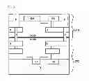
FIG. 2 is a cross-sectional view of a semiconductor device fabricated through a method for electrically connecting wafers according to an embodiment of the present invention;
FIG. 3A illustrates that two wafers are physically bonded to each other;
FIG. 3B illustrates that a first butting contact hole is formed from a substrate of a first wafer to a first conductive region; and
FIG. 3C illustrates that a second butting contact hole is formed from the first conductive region to a second conductive region.
DETAILED DESCRIPTION OF PREFERRED EMBODIMENTS
Reference will now be made in greater detail to a preferred embodiment of the invention, an example of which is illustrated in the accompanying drawings. Wherever possible, the same reference numerals will be used throughout the drawings and the description to refer to the same or like parts.
FIG. 2 is a cross-sectional view of a semiconductor device fabricated through a method for electrically connecting wafers according to an embodiment of the present invention.
Referring to FIG. 2, a physical bonding process for the semiconductor device according to the embodiment of the present invention is implemented through an oxide-to-oxide bonding method. According to the oxide-to-oxide bonding method, upper and lower wafers 210 and 220 covered with oxide are physically bonded to each other. Thus, the two wafers 210 and 220 are electrically insulated from each other. When this method is applied, only the alignment between the two wafers 210 and 220 may be considered. Thus, the bonding process may be relatively easily performed.
FIG. 2 illustrates that the two wafers 210 and 220 are bonded to each other according to the oxide-to-oxide bonding method. However, this is only an example, and the two wafers 210 and 220 may be bonded to each other through another bonding method, instead of the oxide-to-oxide bonding method.
In the conventional semiconductor device of FIG. 1, the bonded portion between the two wafers 110 and 120 is divided into the conductor (Cu) and the oxide. In the embodiment of FIG. 2, however, the entire bonded portion between the two wafers 210 and 220 is oxide. In FIG. 2, F represents a butting contact hole which is formed after physical bonding. The butting contact hole will be described below.
First conductive regions A and C formed in the first wafer 210 are electrically connected to second conducive regions B and D formed in the second wafer 220 through first butting contact holes E formed in the first conductive regions A and C through the substrate of the first wafer 210 and second butting contact holes F formed between the first conductive regions A and C and the second conductive regions B and D, respectively.
The first butting contact hole E is filled with an insulating material, and the second butting contact hole F is filled with a conductive material. Thus, only necessary parts may be electrically connected to each other.
FIG. 2 illustrates the first butting contact hole E has a larger cross-sectional area than the second butting contact hole F. However, the first and second butting contact holes E and F may have the same cross-sectional area. Whether the first and second butting contact holes E and F are formed to have different cross-sectional areas or the same cross-sectional area is not a special technique for those skilled in the art. Thus, the detailed descriptions thereof are omitted herein.
When the first and second butting contact holes E and F are formed, the following process may be commonly performed regardless of whether the first and second butting contact holes E and F have different cross-sectional areas or the same cross-sectional area: a photoresist is applied, a predetermined pattern formed in a mask is reflected onto the photoresist, and the photoresist is baked and then etched.
Hereafter, a process for fabricating the semiconductor device of FIG. 2 will be described.
FIGS. 3A to 3C are cross-sectional views illustrating a process for fabricating the semiconductor device of FIG. 2.
FIG. 3A illustrates that two wafers are physically bonded to each other.
FIG. 3B illustrates that the first butting contact hole is formed from the substrate of the first wafer to the first conductive region.
FIG. 3C illustrates that the second butting contact hole is formed from the first conductive region to the second conductive region.
Referring to FIG. 3A, when two wafers 210 and 220 are physically bonded to each other, oxides formed on the surfaces of the two wafers 210 and 220 are bonded to each other. Thus, this method is referred to as the oxide-to-oxide bonding method, and elements formed in the two wafers 210 and 220 are electrically insulated from each other.
Referring to FIG. 3B, the first butting contact hole E is formed from the substrate of the first wafer 210 to the first conductive regions A and C. During this process, a patterned mask is used to form the first butting contact hole E through a photoresist process and an etch process.
In general, a substrate of a wafer in which semiconductor elements are formed has a considerably large thickness. However, before the first butting contact hole E is formed, the bottom of the substrate of the first wafer 210 is ground to make the thickness of the substrate smaller than the substrate (Si) of the second wafer 220. Referring to FIG. 2, it can be seen that the substrate of the first wafer 210 at the bottom has a larger thickness than the substrate of the second wafer 220 at the top. The first butting contact hole E is formed through an etching process. Thus, as the thickness of the substrate to be etched is small, the etching time decreases.
The time at which the thickness of the substrate of the first wafer 210 is adjusted may be adjusted. The process may be performed before the physical bonding process of FIG. 3A or may be performed before a process of FIG. 3B and after the physical bonding process of FIG. 3A.
Referring to FIG. 3C, the second butting contact hole F is formed from the first conductive regions A and C to the second conductive regions B and D. During this process, a patterned mask is used to form the second butting hole F through a photoresist process and an etching process. When the two butting contact holes E and F are formed to have different cross-sectional areas as illustrated in FIG. 3C, the first and second butting contact holes E and F may be easily distinguished from each other.
As described above, the two butting contact holes E and F may be sequentially formed through the two processes. However, when the two butting contact holes E and F do not need to have different cross-sectional areas, one butting contact hole including two butting contact holes E and F may be formed through one etching process. In this case, since the butting contact hole is formed through one process, the process may be simplified, and the process time may be reduced.
In the present embodiment, through-silicon vias (TSVs) may be used instead of the butting contact holes. According to the TSV method, a silicon wafer is divided into a plurality of chips having a thickness of several tens of micrometers, and the same chips are vertically stacked and connected through a through-electrode. This method has an advantage in that the thickness of chips and the power consumption may be reduced, compared to a conventional wire bonding method in which stacked chips are connected through a wire.
The embodiment of the present invention may obtain the same effect even though any method is applied.
According to the embodiments of the present invention, the wafers are physically bonded to each other through the oxide-to-oxide bonding method which is simpler than the metal-to-metal bonding method, and then electrically connected to through TSVs or butting contact holes. Therefore, since the fabrication process may be simplified, a process error may be reduced, and the product yield may be improved.
Although a preferred embodiment of the present invention has been described for illustrative purposes, those skilled in the art will appreciate that various modifications, additions and substitutions are possible, without departing from the scope and the spirit of the invention as disclosed in the accompanying claims.
Claims
What is claimed is:1. A method for electrically connecting wafers, which electrically connects first and second wafers subjected to a series of processes using a butting contact structure, the method comprising:
physically bonding the first and second wafers through an insulator-to-insulator bonding method; and
electrically connecting a first conductive region of the first wafer to a second conductive region of the second wafer corresponding to the first conductive region through a metal-to-metal bonding method using through-silicon vias (TSVs) or butting contact holes.
2. The method of claim 1, wherein the electrically-connecting of the first conductive region of the first wafer to the second conductive region of the second wafer comprises:
forming a butting contact hole to reach the second conductive region through the substrate bottom of the first wafer and the first conductive region;
filling a conductive material into a part of the butting contact hole corresponding to the first conductive region and a region between the first and second conductive regions; and
filling an insulating material into the other part of the butting contact hole in which the conductive material is not filled.
3. The method of claim 2, wherein the forming of the butting contact hole comprises:
forming a first butting contact hole to reach the first conductive region through the substrate bottom of the first wafer; and
forming a second butting contact hole to reach the second conductive region through the first conductive region.
4. The method of claim 3, wherein the filling of the insulating material comprises filling an insulating material into the first butting contact hole, and
the filling of the conductive material comprises filling a conductive material into the second butting contact hole.
5. The method of claim 4, wherein the first butting contact hole has a larger cross-sectional area than the second butting contact hole.
6. The method of claim 1, further comprising removing the substrate bottom of the first wafer to a predetermined thickness by grinding the substrate bottom of the first wafer.
7. The method of claim 6, wherein the removing of the substrate bottom of the first wafer is performed before the physically-bonding of the first and second wafers or performed before the electrically-bonding of the first conductive region of the first wafer to the second conductive region of the second wafer after the physically-bonding of the first and second wafers.
8. The method of claim 1, wherein the physically-bonding of the first and second wafers comprises physically bonding the first and second wafers through an oxide-to-oxide bonding method.
9. A semiconductor device comprising first and second wafers which are electrically connected to each other through the method of claim 1,
wherein the first wafer comprises one or more of a plurality of elements constituting a CMOS image sensor, and
the second wafer comprises a pixel driving circuit and the other elements of the plurality of elements constituting the CMOS image sensor excluding the elements formed in the first wafer.
10. The semiconductor device of claim 9, wherein the first wafer comprises a photodiode to generate charges corresponding to incident light among the plurality of elements constituting the CMOS image sensor.
Images & Drawings included:
Sources:
- United States Patent and Trademark Office - verify current appl. status at the USPTO↗
Recent applications in this class:
- » 20250293227 2025-09-18
HYBRID RECONSTITUTED PANEL LEVEL PACKAGING - » 20250279405 2025-09-04
POWER MODULE PACKAGE FOR DIRECT COOLING MULTIPLE POWER MODULES - » 20250266417 2025-08-21
SEMICONDUCTOR STRUCTURE AND MANUFACTURING METHOD THEREOF - » 20250266416 2025-08-21
STACKED DIES AND METHODS FOR FORMING BONDED STRUCTURES - » 20250246590 2025-07-31
INTEGRATED DEVICES HAVING MULTIPLE DIE ORIENTATIONS - » 20250233119 2025-07-17
INTEGRATED CIRCUIT PACKAGE AND METHOD OF FORMING SAME - » 20250219043 2025-07-03
SEMICONDUCTOR PACKAGING METHOD, SEMICONDUCTOR ASSEMBLY COMPONENT AND ELECTRONIC DEVICE - » 20250210614 2025-06-26
SEMICONDUCTOR STRUCTURE AND MANUFACTURING METHOD OF THE SAME - » 20250210613 2025-06-26
DIRECT APPLIED INTERPOSER FOR CO-PACKAGED OPTICS - » 20250201798 2025-06-19
PACKAGE STRUCTURE, DIE STRUCTURE AND METHOD FOR FORMING THE PACKAGE STRUCTURE
Recent applications for this Assignee:
- » 20150325618 2015-11-12
CMOS IMAGE SENSOR INCLUDING COLOR MICROLENS, AND METHOD FOR MANUFACTURING SAME - » 20150311239 2015-10-29
CMOS image sensor including infrared pixels having improved spectral properties, and method of manufacturing same - » 20140191357 2014-07-10
Multi-substrate image sensor having a dual detection function