Electronic components on trenched substrates and method of forming same
US20140151849A1
2014-06-05
14/157,755
2014-01-17
✅ Patent granted
US 9,508,789 B2
2016-11-29
-
-
Telly Green
Yuanmin Cai | Andrew M. Calderon | Roberts Mlotkowski Safran Cole & Calderon P.C.
2034-08-04
Abstract:
An electronic module includes a substrate including at least one structure that reduces stress flow through the substrate, wherein the structure includes at least one trench in a surface of the substrate, and a plurality of capacitor legs disposed on an upper surface of the substrate.
Inventors:
- Jennifer V. Muncy 14 🇺🇸 Ridgefield, CT, United States
- Vijayeshwar D. Khanna 35 🇺🇸 Millwood, NY, United States
- Sri M. Sri-Jayantha 98 🇺🇸 Ossining, NY, United States
- Arun Sharma 36 🇺🇸 New Rochelle, NY, United States
- David Questad 7 🇺🇸 Hopewell Junction, NY, United States
- Lorenzo Valdevit 9 🇺🇸 Ithaca, NY, United States
Assignee:
- INTERNATIONAL BUSINESS MACHINES CORPORATION 136,239 🇺🇸 ARMONK, NY, United States
- GLOBALFOUNDRIES Inc. 5,848 Grand Cayman, Cayman Islands
Applicant:
Interested in similar patents?
Get notified when new applications in this technology area are published.
Classification:
H01L28/40 » CPC main
Passive two-terminal components without a potential-jump or surface barrier for integrated circuits; Details thereof; Multistep manufacturing processes therefor Capacitors
H01L49/02 IPC
Solid state devices not provided for in groups - and and not provided for in any other subclass; Processes or apparatus peculiar to the manufacture or treatment thereof or of parts thereof Thin-film or thick-film devices
H05K1/0271 » CPC further
Printed circuits; Details Arrangements for reducing stress or warp in rigid printed circuit boards, e.g. caused by loads, vibrations or differences in thermal expansion
H05K1/0271 » CPC further
Printed circuits; Details Arrangements for reducing stress or warp in rigid printed circuit boards, e.g. caused by loads, vibrations or differences in thermal expansion
H05K3/3442 » CPC further
Apparatus or processes for manufacturing printed circuits; Assembling printed circuits with electric components, e.g. with resistor electrically connecting electric components or wires to printed circuits by soldering; Surface mounted components; Leadless components having edge contacts, e.g. leadless chip capacitors, chip carriers
H01L2224/73204 » CPC further
Indexing scheme for arrangements for connecting or disconnecting semiconductor or solid-state bodies and methods related thereto as covered by; Means for bonding being of different types provided for in two or more of groups; Location after the connecting process on the same surface; Bump and layer connectors the bump connector being embedded into the layer connector
H01L2924/15311 » CPC further
Indexing scheme for arrangements or methods for connecting or disconnecting semiconductor or solid-state bodies as covered by; Details of package parts other than the semiconductor or other solid state devices to be connected; Die mounting substrate; Connection portion the connection portion being formed only on the surface of the substrate opposite to the die mounting surface being a ball array, e.g. BGA
H05K1/0231 » CPC further
Printed circuits; Details; Electrical arrangements not otherwise provided for; Reduction of cross-talk, noise or electromagnetic interference using auxiliary mounted passive components or auxiliary substances Capacitors or dielectric substances
H05K1/0231 » CPC further
Printed circuits; Details; Electrical arrangements not otherwise provided for; Reduction of cross-talk, noise or electromagnetic interference using auxiliary mounted passive components or auxiliary substances Capacitors or dielectric substances
H05K1/111 » CPC further
Printed circuits; Details; Printed elements for providing electric connections to or between printed circuits Pads for surface mounting, e.g. lay-out
H05K1/111 » CPC further
Printed circuits; Details; Printed elements for providing electric connections to or between printed circuits Pads for surface mounting, e.g. lay-out
H05K3/3436 » CPC further
Apparatus or processes for manufacturing printed circuits; Assembling printed circuits with electric components, e.g. with resistor electrically connecting electric components or wires to printed circuits by soldering; Surface mounted components; Leadless components having an array of bottom contacts, e.g. pad grid array or ball grid array components
H05K2201/09036 » CPC further
Indexing scheme relating to printed circuits covered by; Shape and layout; Substrate related Recesses or grooves in insulating substrate
H05K2201/09036 » CPC further
Indexing scheme relating to printed circuits covered by; Shape and layout; Substrate related Recesses or grooves in insulating substrate
H05K2201/10015 » CPC further
Indexing scheme relating to printed circuits covered by; Details of components or other objects attached to or integrated in a printed circuit board; Types of components Non-printed capacitor
H05K2201/10015 » CPC further
Indexing scheme relating to printed circuits covered by; Details of components or other objects attached to or integrated in a printed circuit board; Types of components Non-printed capacitor
H05K2201/10727 » CPC further
Indexing scheme relating to printed circuits covered by; Details of components or other objects attached to or integrated in a printed circuit board; Details of electrical connections of non-printed components, e.g. special leads; Components characterised by their electrical contacts Leadless chip carrier [LCC], e.g. chip-modules for cards
Y10T29/4913 » CPC further
Metal working; Method of mechanical manufacture; Electrical device making; Conductor or circuit manufacturing; On flat or curved insulated base, e.g., printed circuit, etc. Assembling to base an electrical component, e.g., capacitor, etc.
Y10T428/24479 » CPC further
Stock material or miscellaneous articles; Structurally defined web or sheet [e.g., overall dimension, etc.] including variation in thickness
H01L21/02 IPC
Processes or apparatus adapted for the manufacture or treatment of semiconductor or solid state devices or of parts thereof Manufacture or treatment of semiconductor devices or of parts thereof
H05K1/02 IPC
Printed circuits Details
H05K1/02 IPC
Printed circuits Details
H05K1/11 IPC
Printed circuits; Details Printed elements for providing electric connections to or between printed circuits
H05K1/11 IPC
Printed circuits; Details Printed elements for providing electric connections to or between printed circuits
H05K3/34 IPC
Apparatus or processes for manufacturing printed circuits; Assembling printed circuits with electric components, e.g. with resistor electrically connecting electric components or wires to printed circuits by soldering
H05K3/34 IPC
Apparatus or processes for manufacturing printed circuits; Assembling printed circuits with electric components, e.g. with resistor electrically connecting electric components or wires to printed circuits by soldering
Description
BACKGROUND OF THE INVENTION
The present application is a Continuation application of U.S. patent application Ser. No. 12/783,787, filed on May 20, 2010, which is a Continuation application of U.S. patent application Ser. No. 12/099,381, filed on Apr. 8, 2008, which is a Continuation application of U.S. patent application Ser. No. 12/030,274 filed on Feb. 13, 2008, which is a Continuation application of U.S. patent application Ser. No. 11/679,407 filed on Feb. 27, 2007.
FIELD OF THE INVENTION
The present invention generally relates to a method and apparatus for surface-mounting capacitors on electronic (organic) substrates, and more particularly to a method and apparatus for reducing strain in a surface-mounted component.
DESCRIPTION OF THE RELATED ART
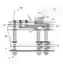
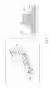
Electronic components, such as capacitors, are typically mounted on a substrate. For example, as illustrated in FIG. 1A, a chip 102 is mounted on a surface of a substrate 104. A plurality of capacitors 106, or other discrete electronic devices, is mounted on the surface of the substrate 104, surrounding the chip 102.
FIG. 1B illustrates a detailed description of the electronic module 100, depicted in FIG. 1A.
Typically, the substrate 104 is formed by first forming the core 108. An entire thickness of the substrate 104 may typically be, approximately 1 mm thick. Next, build-up layers 110 are formed on each of a top surface and a bottom surface of the core 108. The build-up layers typically include polymer and copper layers.
A solder mask 112 is then formed on a surface of the substrate 104. The solder mask 112 covers the substrate, except areas where it is desired to make a solder connection.
The chip (e.g., silicon chip) 102 is mounted to the substrate 104 through solder joints 114. Similarly, the capacitor 106, or other surface mount component, is mounted to the substrate by solder joints 116 and pads 118.
Capacitors that are mounted on a substrate, in accordance with the above description, however, may undergo significant thermomechanical strain. Temperature cycling produces fatigue of the solder joints or cracks in the ceramic plates of the capacitor. Accordingly, the life of the electronic package is reduced.
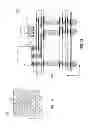
The electronic module is subjected to thermal cycling to evaluate the robustness of the electronic joints. FIG. 2 illustrates the sources of strain on a surface-mounted component during the thermal cycling.
First, shear stress 208 is induced in the solder joints 202, which mount the capacitor 204 to the substrate 206. The shear stress on the solder joints 202 is caused by a mismatch in coefficient of thermal expansion of the capacitor 204 and the substrate 206. Typically, the coefficient of thermal expansion for the capacitor 204 may be on the order of approximately 3 ppm, while the coefficient of thermal expansion of the substrate 206 may be on the order of approximately 20 ppm.
FIG. 3 illustrates the degree of stress 208 on the solder joints 202, the capacitor 204 and the substrate 206. The stress may also produce cracks in the substrate 206.
FIG. 4 illustrates two types of strain induced on the solder joints during thermal cycling. Both Von Mises stress and shear strain are induced on the solder joints.
Returning to FIG. 2, the mismatch in coefficient of thermal expansion also causes the substrate 206 to bend. The bending of the substrate 206 produces a tension/compression stress 210 on the solder joints 202. Additionally, while the bending may reduce the shear stress 208 on the solder joints 202, it will cause an increase in the stress placed on the capacitor 204.
Furthermore, the solder joints 202 have a coefficient of thermal expansion, which may be different from the coefficient of thermal expansion of the capacitor 204 and/or the substrate 206. This mismatch in coefficient of thermal expansion causes a localized, complex stress state 212 on the solder joints 202.
Additionally, the stress at the solder joint areas permeates the body of the electronic components, which can produce cracks that may result in functional failure.
Accordingly, prior to the present invention, there has been no method of surface mounting an electronic component, such as a capacitor, onto a substrate while reducing the effects of stress on the joints, the capacitor and the substrate.
SUMMARY OF THE INVENTION
In view of the foregoing and other exemplary problems, drawbacks, and disadvantages of the conventional methods and structures, an exemplary feature of the present invention is to provide a method and structure in which strain is reduced in a surface-mounted electronic component.
In accordance with a first aspect of the present invention, a method of mounting an electronic component on a substrate includes forming at least one trench in a surface of the substrate.
In accordance with a second aspect of the present invention, an electronic module includes a substrate having at least one trench formed in a surface of the substrate.
In accordance with a third aspect of the present invention, an electronic substrate includes at least one trench in a surface of the electronic substrate.
Forming trenches in a surface of the electronic substrate reduces the stiffness of the substrate in the vicinity of a capacitor (or any other electronic component), so that the substrate has less resistance to shear. Accordingly, the strain on the joints, which mount the electronic component onto the substrate, is reduced, which enhances the life of the joints.
BRIEF DESCRIPTION OF THE DRAWINGS
The foregoing and other exemplary purposes, aspects and advantages will be better understood from the following detailed description of an exemplary embodiment of the invention with reference to the drawings, in which:
FIGS. 1A and 1B illustrate an electronic module 100 including a surface-mounted capacitor 106 mounted according to a conventional mounting technique;
FIG. 2 illustrates typical stresses induced in solder joints 202 of a conventional surface-mounted capacitor 204;
FIG. 3 further illustrates the stress induced on a conventional surface-mounted capacitor;
FIG. 4 further illustrates the stress induced on a conventional surface-mounted capacitor;
FIG. 5 illustrates an exemplary trenched substrate 502 in accordance with an exemplary embodiment of the present invention;
FIG. 6 illustrates a first trench design in accordance with an exemplary embodiment of the present invention;
FIG. 7 illustrates a three-dimensional view of the trench design depicted in FIG. 6;
FIG. 8 graphically depicts the stress reduction resulting from the trenched substrate of the present invention;
FIG. 9 illustrates a second trench design in accordance with an exemplary embodiment of the present invention; and
FIG. 10 illustrates a third trench design in accordance with an exemplary embodiment of the present invention.
DETAILED DESCRIPTION OF EXEMPLARY EMBODIMENTS OF THE INVENTION
Referring now to the drawings, and more particularly to FIGS. 5-10, there are shown exemplary embodiments of the method and structures according to the present invention.
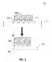
FIG. 5 illustrates an exemplary electronic module 500 in accordance with an exemplary embodiment of the present invention. The electronic module includes a substrate 502 having an electronic component (e.g., capacitor) 506 mounted on a surface of the substrate 502. The capacitor 506 is mounted on the substrate 502 through joints (e.g., solder joints) 504.
In accordance with certain exemplary aspects of the present invention, at least one trench 508 is formed in a surface of the substrate 502. By forming a trench 508 in a surface of the substrate 502, a stiffness of the substrate 502 is reduced. Reducing the stiffness of the substrate 502 reduces the substrate's 502 resistance to shear forces. Accordingly, the stress induced on the substrate 502 and the solder joints 504 is reduced. Therefore, the life of the solder joints 504 is enhanced.
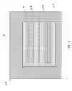
FIG. 6 illustrates a trench design in accordance with an exemplary embodiment of the present invention. FIG. 7 illustrates a three-dimensional view of the electronic module illustrated in FIG. 6.
As shown in FIG. 6, an electronic module 600 includes an electronic component (capacitor) 608 mounted on a substrate 602. The capacitor 608 is mounted to the substrate 602 by a plurality of capacitor legs (solder pads/solder joints) 606.
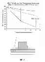
In accordance with the exemplary embodiment depicted in FIG. 6, the capacitor 608 is mounted to the substrate 602 by two rows of solder pads 606. A continuous trench 604 is formed around each row of solder pads 606. Each individual trench is approximately 15 μm deep and is approximately 200 μm wide.
FIG. 8 is a graph depicting the reduction in stress achieved using the trench design illustrated in FIGS. 6 and 7. As indicated in FIG. 8, the trench design depicted in FIGS. 6 and 7 provides an 18% reduction stress.
FIG. 9 illustrates an alternative trench design in accordance with certain exemplary embodiments of the present invention. The trench design depicted in FIG. 9 also includes a continuous trench 902 formed around each row of solder joints 904. Additionally, the trench 902 includes trench extension slits 906 formed between each of the solder joints 904. The trench extension slits 906 further reduce the stiffness of the substrate, thus, further reducing the stress on the solder joints 904.
FIG. 10 illustrates another alternative embodiment of the present invention. Similarly to the embodiments described above, the electronic module 1000 includes a capacitor 1004 mounted to a substrate 1002 by a plurality of capacitor legs 1006. In accordance with the present embodiment, an individual trench 1008 is formed around each of the individual capacitor legs 1006. The trenches 1008 have a shape similar to the shape of the capacitor legs. In the embodiment illustrated in FIG. 10, the trenches have a circular shape.
While the invention has been described in terms of several exemplary embodiments, those skilled in the art will recognize that the invention can be practiced with modification within the spirit and scope of the appended claims.
Further, it is noted that, Applicants' intent is to encompass equivalents of all claim elements, even if amended later during prosecution.
Claims
What is claimed is:1. An electronic module, comprising:
a substrate including at least one structure that reduces stress flow through the substrate, wherein said structure comprises at least one trench in a surface of the substrate; and
a plurality of capacitor legs disposed on an upper surface of the substrate.
2. The electronic module in accordance with claim 1, wherein said at least one trench is formed around the plurality of capacitor legs, said capacitor legs mounting an electronic component to the substrate.
3. The electronic module in accordance with claim 1, wherein said at least one trench comprises:
a first trench formed around a first row of the capacitor legs; and
a second trench formed around a second row of the capacitor legs.
4. The electronic module in accordance with claim 1, wherein said at least one trench comprises a continuous trench.
5. The electronic module in accordance with claim 1, wherein a plurality of continuous trenches are formed around the plurality of capacitor legs.
6. The electronic module in accordance with claim 1, wherein a plurality of individual trenches are formed around the plurality of capacitor legs.
7. The electronic module in accordance with claim 1, wherein the surface comprises the upper surface of the substrate.
8. The electronic module in accordance with claim 1, wherein the surface comprises a surface on which an electronic component is mounted.
9. The electronic module in accordance with claim 1, wherein said at least one trench comprises a plurality of continuous trenches foamed around the plurality of capacitor legs.
10. The electronic module in accordance with claim 1, wherein said trench is formed in the upper surface of the substrate around each of the plurality of capacitor legs.
11. An electronic module, comprising:
a substrate;
an electronic component mounted above the substrate;
a plurality of capacitor legs disposed on an upper surface of the substrate, the plurality of capacitor legs mounting the electronic component above the substrate; and
at least one trench formed around the plurality of capacitor legs.
12. The electronic module according to claim 11, wherein the plurality of capacitor legs comprises a first row of capacitor legs and a second row of capacitor legs, and
wherein the at least one trench comprises one of a plurality of trenches, the plurality of trenches comprising a first trench formed around the first row of capacitor legs and a second trench formed around a second row of capacitor legs.
13. The electronic module according to claim 11, wherein the at least one trench comprises:
a first trench formed around a first row of the capacitor legs; and
a second trench formed around a second row of the capacitor legs.
14. The electronic module according to claim 11, wherein said at least one trench comprises a plurality of individual trenches, said individual trenches being formed around the plurality of capacitor legs.
15. An electronic module, comprising:
a substrate; and
at least one trench in a surface of the substrate, said at least one trench being formed around a plurality of capacitor legs disposed on an upper surface of the substrate, said capacitor legs mounting an electronic component to the substrate.
16. The electronic module in accordance with claim 15, wherein the at least one trench comprises a plurality of trenches.
Images & Drawings included:


Sources:
- United States Patent and Trademark Office - verify current appl. status at the USPTO↗
Similar patent applications:
- » 20080205023
ELECTRONIC COMPONENTS ON TRENCHED SUBSTRATES AND METHOD OF FORMING SAME - » 20080205024
Electronic components on trenched substrates and method of forming same - » 20080218990
Electronic components on trenched substrates and method of forming same - » 20080226875
Electronic components on trenched substrates and method of forming same - » 20090085161
Electronic components on trenched substrates and method of forming same - » 20100276784
Electronic components on trenched substrates and method of forming same
Recent applications in this class:
- » 20250056820 2025-02-13
METAL-INSULATOR-METAL DEVICE WITH HIGH-K LAYER CAPPING STRUCTURE - » 20240387607 2024-11-21
RADIATION RESISTANT SEMICONDUCTOR DEVICE AND METHOD FOR MANUFACTURING SAME - » 20240387606 2024-11-21
METHOD FOR MANUFACTURING CAPACITOR STRUCTURE - » 20240363677 2024-10-31
SEMICONDUCTOR STRUCTURE AND MANUFACTURING METHOD FOR THE SAME - » 20240355869 2024-10-24
COMPOSITE PASSIVE COMPONENT AND PREPARATION METHOD THEREFOR - » 20240347579 2024-10-17
SEMICONDUCTOR DEVICE HAVING CAPACITOR AND MANUFACTURING METHOD THEREOF - » 20240321937 2024-09-26
METHOD OF MANUFACTURING SEMICONDUCTOR DEVICE HAVING CAPACITOR PILLAR - » 20240297209 2024-09-05
FILM FORMING METHOD, METHOD OF MANUFACTURING SEMICONDUCTOR DEVICE, AND PROCESSING SYSTEM - » 20240274650 2024-08-15
CAPACITOR, SEMICONDUCTOR DEVICE INCLUDING THE SAME, AND METHOD OF FABRICATING CAPACITOR - » 20240213302 2024-06-27
INTEGRATED CIRCUIT DEVICE
Recent applications for this Assignee:
- » 20250294045 2025-09-18
THREAT POLICY FINE-TUNING BASED ON THE VULNERABILITY OF A SUBNET AS A SOURCE OF A MALICIOUS ATTACK - » 20250294041 2025-09-18
DEVICE POPULATION ANOMALY DETECTION - » 20250292574 2025-09-18
SCENE PARSING - » 20250292026 2025-09-18
A GENERATIVE ARTIFICIAL INTELLIGENCE COMMENTARY - » 20250291689 2025-09-18
MACHINE LEARNING MODEL TRAINING TO ASSIST IN SYSTEM DEBUG - » 20250287215 2025-09-11
PORTABLE MEDIA GEOFENCE AND DEVICE PAIRING SECURITY - » 20250285610 2025-09-11
RECIPIENT-SPECIFIC VOICE TONE ADJUSTMENT IN TELEPHONY - » 20250284728 2025-09-11
CONTEXT LARGE LANGUAGE MODEL OUTPUT EXPLANATION - » 20250278669 2025-09-04
COUNTERFACTUALS WITH FEATURE PREFERENCES FOR CONSISTENT AND DIVERSE EXPLANATIONS - » 20250274345 2025-08-28
MULTI-LAYER EDGE ARCHITECTURE SIMULATION