Semiconductor device and method for fabricating the same
US20140183559A1
2014-07-03
14/098,409
2013-12-05
✅ Patent granted
US 9,029,872 B2
2015-05-12
-
-
Laura Menz
McDermott Will & Emery LLP
2033-12-05
Abstract:
The present inventive concept has been made in an effort to improve the breakdown voltage of a silicon carbide MOSFET using a trench gate.
A semiconductor device according to the present inventive concept includes a p type pillar region disposed below the trench, spaced apart from the trench or a first p type pillar region and a second p type pillar region disposed below the trench and corresponding to two corners of the trench.
Inventors:
- Jong Seok Lee 40 🇰🇷 Suwon-si, South Korea
- Kyoung-Kook Hong 24 🇰🇷 Hwaseong-si, South Korea
- Youngkyun JUNG 55 🇰🇷 Seoul, South Korea
- Dae Hwan Chun 11 🇰🇷 Gwangmyung-si, South Korea
- Kyoung-Kook HONG 1 🇰🇷 Hwaseong-s, South Korea
Assignee:
- Hyundai Motor Company 20,646 🇰🇷 Seoul, South Korea
Applicant:
Interested in similar patents?
Get notified when new applications in this technology area are published.
Classification:
H01L29/7827 » CPC further
Semiconductor devices adapted for rectifying, amplifying, oscillating or switching, or capacitors or resistors with at least one potential-jump barrier or surface barrier, e.g. PN junction depletion layer or carrier concentration layer; Details of semiconductor bodies or of electrodes thereof; Multistep manufacturing processes therefor; Types of semiconductor device ; Multistep manufacturing processes therefor controllable by only the electric current supplied, or only the electric potential applied, to an electrode which does not carry the current to be rectified, amplified or switched; Unipolar devices, e.g. field effect transistors; Field effect transistors with field effect produced by an insulated gate Vertical transistors
H01L21/02664 » CPC further
Processes or apparatus adapted for the manufacture or treatment of semiconductor or solid state devices or of parts thereof; Manufacture or treatment of semiconductor devices or of parts thereof; Forming layers; Forming inorganic semiconducting materials on a substrate; Special treatments Aftertreatments
H01L21/0475 » CPC further
Processes or apparatus adapted for the manufacture or treatment of semiconductor or solid state devices or of parts thereof; Manufacture or treatment of semiconductor devices or of parts thereof the devices having at least one potential-jump barrier or surface barrier, e.g. PN junction, depletion layer or carrier concentration layer the devices having semiconductor bodies comprising crystalline silicon carbide Changing the shape of the semiconductor body, e.g. forming recesses,
H01L21/02 IPC
Processes or apparatus adapted for the manufacture or treatment of semiconductor or solid state devices or of parts thereof Manufacture or treatment of semiconductor devices or of parts thereof
H01L29/1608 » CPC main
Semiconductor devices adapted for rectifying, amplifying, oscillating or switching, or capacitors or resistors with at least one potential-jump barrier or surface barrier, e.g. PN junction depletion layer or carrier concentration layer; Details of semiconductor bodies or of electrodes thereof; Multistep manufacturing processes therefor; Semiconductor bodies ; Multistep manufacturing processes therefor characterised by the materials of which they are formed including, apart from doping materials or other impurities, only elements of Group IV of the Periodic System Silicon carbide
H01L29/66068 » CPC further
Semiconductor devices adapted for rectifying, amplifying, oscillating or switching, or capacitors or resistors with at least one potential-jump barrier or surface barrier, e.g. PN junction depletion layer or carrier concentration layer; Details of semiconductor bodies or of electrodes thereof; Multistep manufacturing processes therefor; Types of semiconductor device ; Multistep manufacturing processes therefor; Multistep manufacturing processes of devices having a semiconductor body comprising crystalline silicon carbide the devices being controllable only by the electric current supplied or the electric potential applied, to an electrode which does not carry the current to be rectified, amplified or switched, e.g. three-terminal devices
H01L29/16 IPC
Semiconductor devices adapted for rectifying, amplifying, oscillating or switching, or capacitors or resistors with at least one potential-jump barrier or surface barrier, e.g. PN junction depletion layer or carrier concentration layer; Details of semiconductor bodies or of electrodes thereof; Multistep manufacturing processes therefor; Semiconductor bodies ; Multistep manufacturing processes therefor characterised by the materials of which they are formed including, apart from doping materials or other impurities, only elements of Group IV of the Periodic System
H01L29/66 IPC
Semiconductor devices adapted for rectifying, amplifying, oscillating or switching, or capacitors or resistors with at least one potential-jump barrier or surface barrier, e.g. PN junction depletion layer or carrier concentration layer; Details of semiconductor bodies or of electrodes thereof; Multistep manufacturing processes therefor Types of semiconductor device ; Multistep manufacturing processes therefor
H01L29/41766 » CPC further
Semiconductor devices adapted for rectifying, amplifying, oscillating or switching, or capacitors or resistors with at least one potential-jump barrier or surface barrier, e.g. PN junction depletion layer or carrier concentration layer; Details of semiconductor bodies or of electrodes thereof; Multistep manufacturing processes therefor; Electrodes ; Multistep manufacturing processes therefor characterised by their shape, relative sizes or dispositions carrying the current to be rectified, amplified or switched; Source or drain electrodes for field effect devices with at least part of the source or drain electrode having contact below the semiconductor surface, e.g. the source or drain electrode formed at least partially in a groove or with inclusions of conductor inside the semiconductor
H01L21/0455 » CPC further
Processes or apparatus adapted for the manufacture or treatment of semiconductor or solid state devices or of parts thereof; Manufacture or treatment of semiconductor devices or of parts thereof the devices having at least one potential-jump barrier or surface barrier, e.g. PN junction, depletion layer or carrier concentration layer the devices having semiconductor bodies comprising crystalline silicon carbide Making n or p doped regions or layers, e.g. using diffusion
H01L21/00 IPC
Processes or apparatus adapted for the manufacture or treatment of semiconductor or solid state devices or of parts thereof
H01L29/78 IPC
Semiconductor devices adapted for rectifying, amplifying, oscillating or switching, or capacitors or resistors with at least one potential-jump barrier or surface barrier, e.g. PN junction depletion layer or carrier concentration layer; Details of semiconductor bodies or of electrodes thereof; Multistep manufacturing processes therefor; Types of semiconductor device ; Multistep manufacturing processes therefor controllable by only the electric current supplied, or only the electric potential applied, to an electrode which does not carry the current to be rectified, amplified or switched; Unipolar devices, e.g. field effect transistors; Field effect transistors with field effect produced by an insulated gate
H01L29/06 IPC
Semiconductor devices adapted for rectifying, amplifying, oscillating or switching, or capacitors or resistors with at least one potential-jump barrier or surface barrier, e.g. PN junction depletion layer or carrier concentration layer; Details of semiconductor bodies or of electrodes thereof; Multistep manufacturing processes therefor; Semiconductor bodies ; Multistep manufacturing processes therefor characterised by their shape; characterised by the shapes, relative sizes, or dispositions of the semiconductor regions ; characterised by the concentration or distribution of impurities within semiconductor regions
H01L29/417 IPC
Semiconductor devices adapted for rectifying, amplifying, oscillating or switching, or capacitors or resistors with at least one potential-jump barrier or surface barrier, e.g. PN junction depletion layer or carrier concentration layer; Details of semiconductor bodies or of electrodes thereof; Multistep manufacturing processes therefor; Electrodes ; Multistep manufacturing processes therefor characterised by their shape, relative sizes or dispositions carrying the current to be rectified, amplified or switched
H01L21/04 IPC
Processes or apparatus adapted for the manufacture or treatment of semiconductor or solid state devices or of parts thereof; Manufacture or treatment of semiconductor devices or of parts thereof the devices having at least one potential-jump barrier or surface barrier, e.g. PN junction, depletion layer or carrier concentration layer
Description
CROSS-REFERENCE TO RELATED APPLICATION
This application claims benefit of priority to Korean Patent Application No. 10-2012-0155374 filed in the Korean Intellectual Property Office on Dec. 27, 2012, the entire contents of which are incorporated herein by reference.
TECHNICAL FIELD
The present inventive concept relates to a semiconductor device including silicon carbide (SiC) and a method for fabricating the same.
BACKGROUND
With the recent trend toward large-sized and large-capacity application apparatuses, a power semiconductor device having a high breakdown voltage, a high current capacity, and high-speed switching characteristics has become necessary.
Accordingly, many researches and developments are being conducted on MOSFETs (metal oxide semiconductor field effect transistors) using silicon carbide (SiC), instead of conventional MOSFETs using silicon. Particularly, there is a lot of development of vertical trench MOSFETs.
In the case of a vertical trench MOSFET, a breakdown occurs which can damage an oxide film due to an electric field concentration effect by which an electric field is concentrated at the bottom of a gate. This causes a premature breakdown which exhibits a breakdown voltage much lower than a breakdown voltage caused by the intrinsic threshold voltage of a raw material of the MOSFET.
The above information disclosed in this Background section is only for enhancement of understanding of the background of the inventive concept and therefore it may contain information that does not form the prior art.
SUMMARY
The present inventive concept has been made in an effort to improve the breakdown voltage of a silicon carbide MOSFET using a trench gate.
An aspect of the present inventive concept relates to a semiconductor device including: an n+ type silicon carbide substrate; a first p type pillar region and an n− type epitaxial layer disposed on a first surface of the n+ type silicon carbide substrate; a p type epitaxial layer and an n+ region sequentially disposed on the n− type epitaxial layer; a trench penetrating the n+ region and the p type epitaxial layer and disposed on the n− type epitaxial layer; a gate insulating film disposed within the trench; a gate electrode disposed on the gate insulating film; an oxide film disposed on the gate electrode; a source electrode disposed on the p type epitaxial layer, the n+ region, and the oxide film; and a drain electrode positioned on a second surface of the n+ type silicon carbide substrate, wherein the first p type pillar region is disposed within the n− type epitaxial layer, and the first p type pillar region is disposed below the trench, spaced apart from the trench.
The first type pillar region may be disposed in an area corresponding to a portion between two corners of the trench.
The semiconductor according to the present inventive concept may further include a second p type pillar region that is disposed on the first surface of the n+ type silicon carbide substrate and spaced apart from the first p type pillar region.
The second p type pillar region may be spaced apart from the trench, and disposed within the n− type epitaxial layer.
The first p type pillar region and the second p type pillar region may be respectively disposed in areas corresponding to two corners of the trench.
The first p type pillar region and the second p type pillar region may have the same width and length.
Another aspect of the present inventive concept encompasses a method for fabricating a semiconductor device, the method including: forming a buffer layer pattern on a first surface of an n+ type silicon carbide substrate to expose a part of the first surface of the n+ type silicon carbide substrate; forming a first p type pillar region by first epitaxial growth on the exposed part of the first surface of the n+ type silicon carbide substrate; removing the buffer layer pattern, and then forming an n− type epitaxial layer by second epitaxial growth on the first p type pillar region and the first surface of the n+ type silicon carbide substrate; forming a p type epitaxial layer by third epitaxial growth on the n− type epitaxial layer; forming an n+ region by fourth epitaxial growth on the p type epitaxial layer; and forming a trench by penetrating the n+ region and the p type epitaxial layer and etching and the n− type epitaxial layer, wherein the first p type pillar region is formed below the trench, and spaced apart from the trench.
The first type pillar region may be disposed in an area corresponding to a portion between two corners of the trench.
The forming of a first p type pillar region may further include forming a second p type pillar region on the first surface of the n+ type silicon carbide substrate, the first p type pillar region being spaced apart from the first p type pillar region, and positioned within the n− type epitaxial layer.
The first p type pillar region and the second p type pillar region may have the same width and length, and the first p type pillar region and the second p type pillar region may be respectively formed in areas corresponding to two corners of the trench.
The method for fabricating a semiconductor device according to the exemplary embodiment of the present inventive concept may further include: after the forming of an n+ region, forming a gate insulating film within the trench; forming a gate electrode on the gate insulating film; forming an oxide film on the gate insulating film and the gate electrode; and forming a source electrode on the p type epitaxial layer, the n+ region, and the oxide film and forming a drain electrode on the second surface of the n+ type silicon carbide substrate.
According to an exemplary embodiment of the present inventive concept, a p type pillar region is disposed in an area provided below the trench and corresponding to a portion between two corners of the trench, or two p type pillar regions are disposed in areas provided below the trench and corresponding to two corners of the trench. As a result, an electric field concentrated on the gate insulating film at the bottom of the trench spreads to a junction between the p type pillar region and the n− type epitaxial layer.
Accordingly, the breakdown voltage of the semiconductor device can be improved.
BRIEF DESCRIPTION OF THE DRAWINGS
The foregoing and other features of the inventive concept will be apparent from a more particular description of embodiments of the inventive concept, as illustrated in the accompanying drawings in which like reference characters may refer to the same or similar parts throughout the different views. The drawings are not necessarily to scale, emphasis instead being placed upon illustrating the principles of the embodiments of the inventive concept.
FIG. 1 is a cross-sectional view of a semiconductor device according to an exemplary embodiment of the present inventive concept.
FIG. 2 to FIG. 7 are views sequentially showing a method for fabricating a semiconductor device according to an exemplary embodiment of the present inventive concept.
FIG. 8 is a graph comparing the breakdown voltage of a semiconductor device according to an exemplary embodiment of the present inventive concept with the breakdown voltage of a conventional semiconductor device.
FIG. 9 is a cross-sectional view of a semiconductor device according to another exemplary embodiment of the present inventive concept.
DETAILED DESCRIPTION
Exemplary embodiments of the present inventive concept will be described in detail with reference to the attached drawings. The present inventive concept may be modified in many different forms and should not be construed as being limited to the exemplary embodiments set forth herein. Rather, the exemplary embodiments of the present inventive concept are provided so that this disclosure will be thorough and complete, and will fully convey the concept of the present inventive concept to those skilled in the art.
In the drawings, the thickness of layers and regions may be exaggerated for clarity. In addition, when a layer is described to be formed on another layer or on a substrate, this means that the layer may be formed on the other layer or on the substrate, or a third layer may be interposed between the layer and the other layer or the substrate. Like numbers refer to like elements throughout the specification.
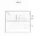
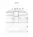
FIG. 1 is a cross-sectional view of a semiconductor device according to an exemplary embodiment of the present inventive concept.
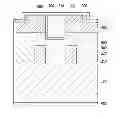
Referring to FIG. 1, the semiconductor device according to an exemplary embodiment of the present inventive concept may have a p type pillar region 200 and an n− type epitaxial layer 300 disposed on a first surface of an n+ type silicon carbide substrate 100. The p type pillar region 200 may be disposed within the n− type epitaxial layer 300.
A p type epitaxial layer 400 and an n+ region 500 may be sequentially disposed on the n− type epitaxial layer 300.
A trench 550 may be disposed in the n− type epitaxial layer 300, the p type epitaxial layer 400, and the n+ region 500. The trench 550 may penetrate the n+region 500 and the p type epitaxial layer 400.
The p type pillar region 200 may be spaced apart from the trench 550, and disposed in an area provided below the trench 550 and corresponding to a portion between two corners of the trench 550.
A gate insulating film 600 may be disposed within the trench 550, a gate electrode 700 may be disposed on the gate insulating film 600, and an oxide film 610 may be disposed on the gate insulating film 600 and the gate electrode 700. The gate electrode 700 may fill the trench 550.
A source electrode 800 may be formed on the p type epitaxial layer 400, the n+ region 500, and the oxide film 610. A drain electrode 900 may be formed on a second surface of the n+ type silicon carbide substrate 100.
As the p type pillar region 200 may be disposed in an area provided below the trench 550 and corresponding to a portion between two corners of the trench 550, an electric field concentrated on the gate insulating film 600 may spread by a junction between the p type pillar region 200 and the n− type epitaxial layer 300. As a result, the breakdown voltage can be improved.
Now, a method for fabricating a semiconductor device according to one exemplary embodiment of the present inventive concept will be described with reference to FIGS. 2 to 7 and FIG. 1.
FIG. 2 to FIG. 7 are views sequentially showing a method for fabricating a semiconductor device according to an exemplary embodiment of the present inventive concept.
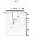
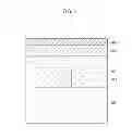
As shown in FIG. 2, an n+ type silicon carbide substrate 100 may be prepared, and a buffer layer pattern 50 may be formed on a first surface of the n+ type silicon carbide substrate 100. The buffer layer pattern 50 may expose a part of the first surface of the n+ type silicon carbide substrate 100.
As shown in FIG. 3, a plurality of p type pillar regions 200 may be formed by first epitaxial growth on the exposed part of the first surface of the n+ type silicon carbide substrate 100.
As shown in FIG. 4, the buffer layer pattern 50 may be removed, and then an n− type epitaxial layer 300 may be formed by second epitaxial growth on the p type pillar region 200 and the first surface of the n+ type silicon carbide substrate 100.
As shown in FIG. 5, a p type epitaxial layer 400 may be formed by third epitaxial growth on the n− type epitaxial layer 300, and then an n+ region 500 may be formed by fourth epitaxial growth on the p type epitaxial layer 400.
The n+ region 500 may be formed by the fourth epitaxial growth in an exemplary embodiment of the present inventive concept. Alternatively, the n+ region 500 may be formed by implanting n+ ions into part of the surface of the p type epitaxial layer 400, without performing epitaxial growth.
As shown in FIG. 6, a trench 550 may be formed by etching a part of the n+ region 500, the p type epitaxial layer 400, and the n− type epitaxial layer 300. The trench 550 may penetrate the n+ region 500 and the p type epitaxial layer 400. The p type pillar region 200 may be positioned below the trench 550, spaced apart from the trench 550. Also, the p type pillar region 200 may be positioned in an area corresponding to a portion between two corners of the trench 550.
As shown in FIG. 7, a gate insulating film 600 may be formed within the trench 550, and a gate electrode 700 may be formed on the gate insulating film 600. An oxide film 610 may be formed on the gate insulating film 600 and the gate electrode 700, and part of the n+ region 500 is etched.
As shown in FIG. 1, a source electrode 800 may be formed on the p type epitaxial layer 400, the n+ region 500, and the oxide film 610, and a drain electrode 850 is formed on a second surface of the n+ type silicon carbide substrate 100.
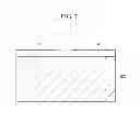
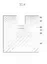
Now, the characteristics of a semiconductor according to an exemplary embodiment of the present inventive concept and of a conventional semiconductor device will be described in detail with reference to FIG. 8.
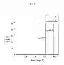
FIG. 8 is a graph comparing the breakdown voltage of a semiconductor device according to an exemplary embodiment of the present inventive concept with the breakdown voltage of a conventional semiconductor device.
In FIG. 8, A represents a typical vertical trench MOSFET according to the conventional art, i.e., a vertical trench MOSFET having no p type pillar region disposed below the trench, and B represents a semiconductor device according to an exemplary embodiment of the present inventive concept.
Referring to FIG. 8, the breakdown voltage of the typical vertical trench MOSFET according to the conventional art was 1550 V, and the breakdown voltage of the semiconductor device according to one exemplary embodiment of the present inventive concept was 1961 V.
Based upon this, it can be concluded that the breakdown voltage of the semiconductor device according to an exemplary embodiment of the present inventive concept was compared with the breakdown voltage of the conventional semiconductor device. The result shows that the breakdown voltage of the semiconductor device according to an exemplary embodiment of the present inventive concept was about 27% higher than the breakdown voltage of the typical vertical trench MOSFET according to the conventional art. This means that the breakdown voltage of the semiconductor device according to an exemplary embodiment of the present inventive concept was improved, compared with the breakdown voltage of the typical semiconductor device according to the conventional art.
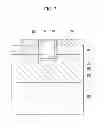
Now, a semiconductor device according to another exemplary embodiment of the present inventive concept will be described with reference to FIG. 9.
FIG. 9 is a cross-sectional view of a semiconductor device according to another exemplary embodiment of the present inventive concept.
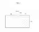
Referring to FIG. 9, the semiconductor device according to an exemplary embodiment of the present inventive concept is identical to the semiconductor device of FIG. 1, except that a first p type pillar region 210 and a second p type pillar region 220 may be disposed on a first surface of an n+ type silicon carbide substrate 100.
In the semiconductor device according to an exemplary embodiment of the present inventive concept, a first p type pillar region 210, a second p type pillar region 220, and an n− type epitaxial layer 300 may be disposed on a first surface of an n+ type silicon carbide substrate 100. The first p type pillar region 210 and the second p type pillar region 220 may be spaced apart from each other, and disposed within the n− type epitaxial layer 300. The first p type pillar region 210 and the second p type pillar region 200 may have the same width and length. Moreover, the first p type pillar region 210 and the second p type pillar region 220 may be simultaneously formed during the same epitaxial growth.
A p type epitaxial layer 400 and an n+ region 500 may be sequentially disposed on the n− type epitaxial layer 300.
A trench 550 may be disposed in the n− type epitaxial layer 300, the p type epitaxial layer 400, and the n+ region 500. The trench 550 may penetrate the n+ region 500 and the p type epitaxial layer 400.
The first p type pillar region 210 and the second p type pillar region 220 may be spaced apart from the trench 550, and disposed in areas provided below the trench 550 and corresponding to two corners of the trench 550.
A gate insulating film 600 may be disposed within the trench 550, a gate electrode 700 may be disposed on the gate insulating film 600, and an oxide film 610 may be disposed on the gate insulating film 600 and the gate electrode 700. The gate electrode 700 may fill the 550.
A source electrode 800 may be formed on the p type epitaxial layer 400, the n+ region 500, and the oxide film 610. A drain electrode 900 may be formed on a second surface of the n+ type silicon carbide substrate 100.
As the first p type pillar region 210 and the second p type pillar region 220 may be disposed in areas provided below the trench 550 and corresponding to two corners of the trench 550, an electric field concentrated on the gate insulating film 600 at the bottom of the trench 550 may spread by a junction between the first and second p type pillar regions 210 and 220 and the n− type epitaxial layer 300. As a result, the breakdown voltage can be improved.
While this inventive concept has been described in connection with what is presently considered to be practical exemplary embodiments, it is to be understood that the inventive concept is not limited to the disclosed embodiments, but, on the contrary, is intended to cover various modifications and equivalent arrangements included within the spirit and scope of the appended claims.
DESCRIPTION OF SYMBOLS
| 50: buffer layer pattern | |
| 100: n+ type silicon carbide substrate | |
| 200: p type pillar region | 210: first p type pillar region |
| 220: second p type pillar region | 300: n− type epitaxial layer |
| 400: p type epitaxial layer | 500: n+ region |
| 550: trench | 600: gate insulating film |
| 610: oxide film | 700: gate electrode |
| 800: source electrode | 900: drain electrode |
While this inventive concept has been described in connection with what is presently considered to be practical exemplary embodiments, it is to be understood that the inventive concept is not limited to the disclosed embodiments, but, on the contrary, is intended to cover various modifications and equivalent arrangements included within the spirit and scope of the appended claims.
Claims
What is claimed is:1. A semiconductor device, comprising:
an n+ type silicon carbide substrate;
a first p type pillar region and an n− type epitaxial layer, disposed on a first surface of the n+ type silicon carbide substrate;
a p type epitaxial layer and an n+ region, sequentially disposed on the n− type epitaxial layer;
a trench penetrating the n+ region and the p type epitaxial layer and disposed on the n− type epitaxial layer;
a gate insulating film disposed within the trench;
a gate electrode disposed on the gate insulating film;
an oxide film disposed on the gate electrode;
a source electrode disposed on the p type epitaxial layer, the n+ region, and the oxide film; and
a drain electrode positioned on a second surface of the n+ type silicon carbide substrate, wherein:
the first p type pillar region is disposed within the n− type epitaxial layer, and the first p type pillar region is disposed below the trench, spaced apart from the trench.
2. The semiconductor device of claim 1, wherein the first type pillar region is disposed in an area corresponding to a portion between two corners of the trench.
3. The semiconductor device of claim 1, further comprising a second p type pillar region that is disposed on the first surface of the n+ type silicon carbide substrate and spaced apart from the first p type pillar region.
4. The semiconductor device of claim 3, wherein the second p type pillar region is spaced apart from the trench, and disposed within the n− type epitaxial layer.
5. The semiconductor device of claim 4, wherein the first p type pillar region and the second p type pillar region are respectively disposed in areas corresponding to two corners of the trench.
6. The semiconductor device of claim 5, wherein the first p type pillar region and the second p type pillar region have the same width and length.
7. A method for fabricating a semiconductor device, the method comprising:
forming a buffer layer pattern on a first surface of an n+ type silicon carbide substrate to expose a part of the first surface of the n+ type silicon carbide substrate;
forming a first p type pillar region by first epitaxial growth on the exposed part of the first surface of the n+ type silicon carbide substrate;
removing the buffer layer pattern, and then forming an n− type epitaxial layer by second epitaxial growth on the first p type pillar region and the first surface of the n+ type silicon carbide substrate;
forming a p type epitaxial layer by third epitaxial growth on the n− type epitaxial layer;
forming an n+ region by fourth epitaxial growth on the p type epitaxial layer; and
forming a trench by penetrating the n+ region and the p type epitaxial layer and by etching a part of the n− type epitaxial layer,
wherein the first p type pillar region is formed below the trench, and spaced apart from the trench.
8. The method of claim 7, wherein the first type pillar region is disposed in an area corresponding to a portion between two corners of the trench.
9. The method of claim 7, wherein the forming of a first p type pillar region further comprises:
forming a second p type pillar region on the first surface of the n+ type silicon carbide substrate, the first p type pillar region being spaced apart from the first p type pillar region, and positioned within the n− type epitaxial layer.
10. The method of claim 9, wherein
the first p type pillar region and the second p type pillar region have the same width and length, and
the first p type pillar region and the second p type pillar region are respectively formed in areas corresponding to two corners of the trench.
11. The method of claim 7, further comprising:
after the forming of an n+ region, forming a gate insulating film within the trench;
forming a gate electrode on the gate insulating film;
forming an oxide film on the gate insulating film and the gate electrode; and
forming a source electrode on the p type epitaxial layer, the n+ region, and the oxide film and forming a drain electrode on the second surface of the n+ type silicon carbide substrate.
Images & Drawings included:
Sources:
- United States Patent and Trademark Office - verify current appl. status at the USPTO↗
Similar patent applications:
- » 20120112209
SILICON CARBIDE SUBSTRATE FABRICATION METHOD, SEMICONDUCTOR DEVICE FABRICATION METHOD, SILICON CARBIDE SUBSTRATE, AND SEMICONDUCTOR DEVICE - » 20080315254
Semiconductor device fabrication method, semiconductor device, and semiconductor layer formation method - » 20060043570
Substrate, semiconductor device, substrate fabricating method, and semiconductor device fabricating method - » 20050014377
Semiconductor device fabrication method and semiconductor device fabrication system for minimizing film-thickness variations - » 20080203440
Semiconductor device fabrication method and semiconductor device fabricated thereby - » 10129305
Semiconductor device fabrication method and semiconductor device fabrication apparatus - » 20060118952
Micro-hole plating method, gold bump fabrication method and semiconductor device fabrication method using the micro-hole plating method, semiconductor device - » 10107298
Semiconductor device fabrication method and semiconductor device - » 20060084251
Plating method, semiconductor device fabrication method and circuit board fabrication method - » 20060084253
Plating method, semiconductor device fabrication method and circuit board fabrication method
Recent applications in this class:
- » 20250063785 2025-02-20
SILICON CARBIDE DIODE WITH REDUCED VOLTAGE DROP, AND MANUFACTURING METHOD THEREOF - » 20250063784 2025-02-20
PROCESS FOR THE MANUFACTURE OF A SEMICONDUCTOR STRUCTURE COMPRISING A POLYCRYSTALLINE SILICON CARBIDE SUBSTRATE AND AN ACTIVE LAYER OF SINGLE-CRYSTAL SILICON CARBIDE - » 20250056856 2025-02-13
SILICON CARBIDE SUBSTRATE, METHOD OF MANUFACTURING SILICON CARBIDE SEMICONDUCTOR DEVICE, AND METHOD OF MANUFACTURING SILICON CARBIDE SUBSTRATE - » 20250040211 2025-01-30
SiC SEMICONDUCTOR DEVICE - » 20250022920 2025-01-16
SIC SEMICONDUCTOR DEVICE - » 20250022919 2025-01-16
DOPING ACTIVATION AND OHMIC CONTACT FORMATION IN A SiC ELECTRONIC DEVICE, AND SiC ELECTRONIC DEVICE - » 20250022918 2025-01-16
SEMICONDUCTOR DIE WITH A SILICON CARBIDE SUBSTRATE - » 20250015139 2025-01-09
SiC SUBSTRATE AND SiC EPITAXIAL WAFER - » 20250015138 2025-01-09
SEMICONDUCTOR DEVICE AND METHOD OF MANUFACTURING THE SAME - » 20250006797 2025-01-02
SiC SEMICONDUCTOR DEVICE
Recent applications for this Assignee:
- » 20250293967 2025-09-18
VEHICLE CONTROL APPARATUS AND METHOD THEREOF - » 20250293557 2025-09-18
MOTOR WITH A COOLING STRUCTURE - » 20250293373 2025-09-18
BATTERY ASSEMBLY - » 20250293361 2025-09-18
FUEL CELL POWER GENERATION MODULE - » 20250293308 2025-09-18
ELECTRODE ASSEMBLY AND ALL-SOLID STATE BATTERY INCLUDING THE SAME - » 20250292638 2025-09-18
SYSTEM AND METHOD FOR MONITORING POWER OF A VEHICLE - » 20250292590 2025-09-18
METHOD AND APPARATUS FOR CONTEXT-RECOGNITION OBJECT ACTION PREDICTION AND PATH PLANNING FOR AUTONOMOUS VEHICLES BASED ON PEDESTRIAN MOTION PREDICTION - » 20250290600 2025-09-18
PRESSURE VESSEL - » 20250289441 2025-09-18
METHOD AND APPARATUS FOR CALIBRATING ORIENTATION ANGLE OF VEHICLE SENSOR - » 20250289422 2025-09-18
SYSTEM AND METHOD FOR GENERATING EMERGENCY COLLISION AVOIDANCE STRATEGY FOR A VEHICLE