Connector / cable assembly
US20140203833A1
2014-07-24
13/749,155
2013-01-24
✅ Patent granted
US 9,297,830 B2
2016-03-29
-
-
Daniel Miller
Brian J. Colandreo | Michael T. Abramson | Holland & Knight LLP
2034-09-21
Abstract:
A high voltage connector assembly includes a plurality of pin assemblies, each of the plurality of pin assemblies having a first end and a second end. The first end of each of the plurality of pin assemblies is configured to releasably electrically engage a load board. A plurality of pin pads, wherein the second end of each of the plurality of pin assemblies is configured to electrically engage a pin pad included within the plurality of pin pads. A plurality of connector pads are electrically coupled to the plurality of pin pads, wherein each of the plurality of connector pads is configured to be electrically coupled to a wire-based conductor included within a plurality of wire-based conductors. A potting compound is configured to encapsulate the plurality of connector pads.
Inventors:
- Richard McCarthy 1 🇺🇸 Raynham, MA, United States
- Christopher Joel Hannaford 4 🇺🇸 Norwood, MA, United States
- Lisette J. Zarzalejo 1 🇺🇸 San Jose, CA, United States
- Roger H. Therrien 1 🇺🇸 Hanover, MA, United States
Assignee:
- LTX-Credence Corporation 13 🇺🇸 Norwood, MA, United States
- Xcerra Corporation 3 🇺🇸 Boston, MA, United States
Applicant:
Interested in similar patents?
Get notified when new applications in this technology area are published.
Classification:
G01R1/0416 » CPC main
Details of instruments or arrangements of the types included in groups - and; General constructional details; Housings; Supporting members; Arrangements of terminals; Test fixtures or contact fields; Connectors or connecting adaptors; Test clips; Test sockets Connectors, terminals
G01R1/04 IPC
Details of instruments or arrangements of the types included in groups - and; General constructional details Housings; Supporting members; Arrangements of terminals
H01R13/2421 » CPC further
Details of coupling devices of the kinds covered by groups or -; Contact members; Contacts for co-operating by abutting resilient; resiliently-mounted characterized by the resilient means using coil springs
G01R1/06722 » CPC further
Details of instruments or arrangements of the types included in groups - and; General constructional details; Measuring leads; Measuring probes; Measuring probes; Probe needles; Cantilever beams; "Bump" contacts; Replaceable probe pins; Elastic Spring-loaded
G01R1/06777 » CPC further
Details of instruments or arrangements of the types included in groups - and; General constructional details; Measuring leads; Measuring probes; Measuring probes High voltage probes
H01R12/714 » CPC further
Structural associations of a plurality of mutually-insulated electrical connecting elements, specially adapted for printed circuits, e.g. printed circuit boards [PCBs], flat or ribbon cables, or like generally planar structures, e.g. terminal strips, terminal blocks; Coupling devices specially adapted for printed circuits, flat or ribbon cables, or like generally planar structures; Terminals specially adapted for contact with, or insertion into, printed circuits, flat or ribbon cables, or like generally planar structures; Coupling devices for rigid printing circuits or like structures co-operating with the surface of the printed circuit or with a coupling device exclusively provided on the surface of the printed circuit with contacts abutting directly the printed circuit; Button contacts therefore provided on the printed circuit
H01R2201/20 » CPC further
Connectors or connections adapted for particular applications for testing or measuring purposes
G01R31/00 IPC
Arrangements for testing electric properties; Arrangements for locating electric faults; Arrangements for electrical testing characterised by what is being tested not provided for elsewhere
H01R13/24 IPC
Details of coupling devices of the kinds covered by groups or -; Contact members; Contacts for co-operating by abutting resilient; resiliently-mounted
G01R1/067 IPC
Details of instruments or arrangements of the types included in groups - and; General constructional details; Measuring leads; Measuring probes Measuring probes
H01R12/71 IPC
Structural associations of a plurality of mutually-insulated electrical connecting elements, specially adapted for printed circuits, e.g. printed circuit boards [PCBs], flat or ribbon cables, or like generally planar structures, e.g. terminal strips, terminal blocks; Coupling devices specially adapted for printed circuits, flat or ribbon cables, or like generally planar structures; Terminals specially adapted for contact with, or insertion into, printed circuits, flat or ribbon cables, or like generally planar structures; Coupling devices for rigid printing circuits or like structures
H01R12/73 » CPC further
Structural associations of a plurality of mutually-insulated electrical connecting elements, specially adapted for printed circuits, e.g. printed circuit boards [PCBs], flat or ribbon cables, or like generally planar structures, e.g. terminal strips, terminal blocks; Coupling devices specially adapted for printed circuits, flat or ribbon cables, or like generally planar structures; Terminals specially adapted for contact with, or insertion into, printed circuits, flat or ribbon cables, or like generally planar structures; Coupling devices for rigid printing circuits or like structures coupling with the edge of the rigid printed circuits or like structures connecting to other rigid printed circuits or like structures
Description
TECHNICAL FIELD
This disclosure relates to electrical connectors and, more particularly, to electrical connectors for use with high-voltage signals.
BACKGROUND
Electrical connections between subassemblies may be achieved using standard electrical connectors, such as a molded housing that includes male/female connectors that are configured to mate with corresponding female/male connector. In such an interconnection scheme, a printed circuit assembly (PCA) may be populated with connectors that are configured to mate with a connector assembly on a cable.
The above-described high-voltage type of interconnections system has performance/cost limitations when used with Automatic Testing Equipment (ATE), as such connections tend to be bulky and expensive.
SUMMARY OF DISCLOSURE
In one implementation, a high voltage connector assembly includes a plurality of pin assemblies, each of the plurality of pin assemblies having a first end and a second end. The first end of each of the plurality of pin assemblies is configured to releasably electrically engage a load board. A plurality of pin pads, wherein the second end of each of the plurality of pin assemblies is configured to electrically engage a pin pad included within the plurality of pin pads. A plurality of connector pads are electrically coupled to the plurality of pin pads, wherein each of the plurality of connector pads is configured to be electrically coupled to a wire-based conductor included within a plurality of wire-based conductors. A potting compound is configured to encapsulate the plurality of connector pads.
One or more of the following features may be included. The load board may be configured to releasable engage one or more devices under test (DUTs). The pin assemblies may be pogo pin assemblies. The plurality of pin pads and the plurality of connector pads may be included on a connector circuit board. The plurality of pin pads and the plurality of connector pads may be positioned on opposite sides of the connector circuit board. The wire-based conductor may be soldered to a connector pad included within the plurality of connector pads. The plurality of wire-based conductors may be included within a multi-conductor cable assembly. A pin alignment structure may be configured to position the plurality of pin assemblies with respect to each other.
In another implementation, a high voltage connector assembly includes a plurality of pogo pin assemblies, each of the plurality of pin assemblies having a first end and a second end. The first end of each of the plurality of pin assemblies is configured to releasably electrically engage a load board that is configured to releasable engage one or more devices under test (DUTs). A plurality of pin pads, wherein the second end of each of the plurality of pin assemblies is configured to electrically engage a pin pad included within the plurality of pin pads. A plurality of connector pads are electrically coupled to the plurality of pin pads. Each of the plurality of connector pads is configured to be electrically coupled to a wire-based conductor included within a plurality of wire-based conductors. A potting compound is configured to encapsulate the plurality of connector pads.
One or more of the following features may be included. The plurality of pin pads and the plurality of connector pads may be included on a connector circuit board. The plurality of pin pads and the plurality of connector pads may be positioned on opposite sides of the connector circuit board. The wire-based conductor may be soldered to a connector pad included within the plurality of connector pads. The plurality of wire-based conductors may be included within a multi-conductor cable assembly. A pin alignment structure may be configured to position the plurality of pin assemblies with respect to each other.
In another implementation, a high voltage cable assembly includes a multi-conductor cable assembly, a PCB connector assembly coupled to a first end of the multi-conductor cable assembly, and a high voltage connector assembly coupled to a second end of the multi-conductor cable assembly. The high voltage connector assembly includes a plurality of pin assemblies, each of the plurality of pin assemblies having a first end and a second end. The first end of each of the plurality of pin assemblies is configured to releasably electrically engage a load board. A plurality of pin pads, wherein the second end of each of the plurality of pin assemblies is configured to electrically engage a pin pad included within the plurality of pin pads. A plurality of connector pads are electrically coupled to the plurality of pin pads, wherein each of the plurality of connector pads is configured to be electrically coupled to a wire-based conductor included within the multi-conductor cable assembly. A potting compound is configured to encapsulate the plurality of connector pads.
One or more of the following features may be included. The load board may be configured to releasable engage one or more devices under test (DUTs). The pin assemblies may be pogo pin assemblies. The plurality of pin pads and the plurality of connector pads may be included on a connector circuit board. The plurality of pin pads and the plurality of connector pads may be positioned on opposite sides of the connector circuit board. The wire-based conductor may be soldered to a connector pad included within the plurality of connector pads. A pin alignment structure may be configured to position the plurality of pin assemblies with respect to each other.
The details of one or more implementations are set forth in the accompanying drawings and the description below. Other features and advantages will become apparent from the description, the drawings, and the claims.
BRIEF DESCRIPTION OF THE DRAWINGS
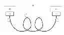
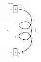
FIG. 1 is a diagrammatic view of a high voltage cable assembly;
FIGS. 2A & 2B are diagrammatic views of a high voltage connector assembly included within the high voltage cable assembly of FIG. 1;
FIG. 3 is a diagrammatic view of a pin assembly included within the high voltage connector assembly of FIGS. 2A & 2B;
FIG. 4 is an isometric view of a pin alignment structure included within the high voltage connector assembly of FIGS. 2A & 2B; and
FIGS. 5A & 5B are diagrammatic views of a connector circuit board included within the high voltage connector assembly of FIGS. 2A & 2B.
Like reference symbols in the various drawings indicate like elements.
DETAILED DESCRIPTION OF THE PREFERRED EMBODIMENTS
Referring to FIG. 1, there is shown high voltage cable assembly 10 that may include multi-conductor cable assembly 12, PCB connector assembly 14 coupled to first end 16 of multi-conductor cable assembly 12, and high voltage connector assembly 18 coupled to a second end 20 of multi-conductor cable assembly 12. As will be discussed below in greater detail, high voltage cable assembly 10 may be configured to connect automated testing equipment 22 to components 24 that are being tested, and transmit high voltage signals (e.g., >1,000 volts) therebetween.
Referring also to FIGS. 2A, 2B & 3, high voltage connector assembly 18 may include plurality of pin assemblies 26. An example of the individual pin assemblies (e.g., pin assembly 28) included within plurality of pin assemblies 26 may include but is not limited to pogo pin assemblies. As is known in the art, a pogo pin assembly is a device used in electronics/electrical circuits to establish a connection (typically a temporary connection) between two electrical circuits (e.g., printed circuit boards). Another example of the individual pin assemblies (e.g., pin assembly 28) included within plurality of pin assemblies 26 may include but is not limited to a low profile, elastomeric pin assembly that incorporate a resilient material to bias distal ends of pin assembly 28 with respect to each other.
Each of the plurality of pin assemblies 26 (e.g., pin assembly 28) may include first end 30 and second end 32. Pin assembly 28 may also include spring-loaded cylinder 34, which may bias first end 30 and second end 32 away from each other. When compressed between two electrical circuits (circuits 36, 38), first end 30 and second end 32 at each end of pin assembly 28 may establish (e.g., temporary) electrical connections with these two electrical circuits (circuits 36, 38 respectively), thereby temporarily electrically coupling circuits 36, 38.
High voltage connector assembly 18 may include pin alignment structure 40, which may be configured to position plurality of pin assemblies 26 with respect to each other. For example and as shown in FIG. 4, pin alignment structure 40 may be configured as a matrix that forms a plurality of channels (e.g., channel 42) into which a pin assembly (e.g., pin assembly 28) included within plurality of pin assemblies 26 is positioned.
The first end (e.g., first end 30) of each of plurality of pin assemblies 26 may be configured to releasably electrically engage load board 44. Load board 44 may be a printed circuit board and may be configured to releasable engage one or more devices under test (DUTs), such as DUTs 46, 48, 50, 52.
Referring also to FIGS. 5A & 5B, high voltage connector assembly 18 may further include connector circuit board 54, wherein connector circuit board 54 includes plurality of pin pads 56 that may be electrically coupled to plurality of connector pads 58. For example, plurality of pin pads 56 and plurality of connector pads 58 may be positioned on opposite sides of connector circuit board 54, wherein electrical conductors (e.g., conductor 60) may pass through connector circuit board 54 and may electrically couple related pairs of pin pads and connector pads. The second end (e.g., second end 32) of each of plurality of pin assemblies 26 may be configured to electrically engage a pin pad included within plurality of pin pads 56.
Pin alignment structure 40 may be configured so that plurality of pin assemblies 26 positioned within pin alignment structure 40 are properly spaced to ensure that e.g., plurality of pin pads 56 are positioned in such a manner to avoid any arcing/shorting or similar undesirable conditions during use of high voltage connector assembly 18.
Each of plurality of connector pads 58 may be configured to be electrically coupled to a wire-based conductor (e.g., wire 62) included within plurality of wire-based conductors 64 (e.g., which may be included within multi-conductor cable assembly 12). The wire-based conductor (e.g., wire 62) may be soldered to a connector pad included within plurality of connector pads 58. Accordingly and as shown in FIGS. 5A & 5B, each of the plurality of connector pads 58 included within connector circuit board 54 may be larger than each of the plurality of pin pads 56 included within connector circuit board 54. Accordingly, the spacing between adjacent connector pads may be smaller than the spacing between adjacent pin pads.
As discussed above, high voltage cable assembly 10 may be configured to connect automated testing equipment 22 to components 24 that are being tested, and may transmit high voltage signals therebetween. Accordingly, as the distance between adjacent connector pads decreases, the likelihood of signals arcing between adjacent connector pads increases. Accordingly, high voltage connector assembly 18 may include potting compound 66 that may be configured to encapsulate plurality of connector pads 58 (and possibly a portion of plurality of wire-based conductors 64), thus isolating/insulting adjacent connector pads from each other and reducing the likelihood of arcing therebetween.
One or more alignment pins (e.g., alignment pins 68, 70) may be utilized to align load board 44 and high voltage connector assembly 18. For example, alignment pins 68, 70 may be tapered alignment pins that are sized to fit within passages in load board 44, thus ensuring proper electrical connectivity with plurality of pin assemblies 26.
A number of implementations have been described. Having thus described the disclosure of the present application in detail and by reference to embodiments thereof, it will be apparent that modifications and variations are possible without departing from the scope of the disclosure defined in the appended claims.
Claims
What is claimed is:1. A high voltage connector assembly comprising:
a plurality of pin assemblies, each of the plurality of pin assemblies having a first end and a second end, wherein the first end of each of the plurality of pin assemblies is configured to releasably electrically engage a load board;
a plurality of pin pads, wherein the second end of each of the plurality of pin assemblies is configured to electrically engage a pin pad included within the plurality of pin pads;
a plurality of connector pads electrically coupled to the plurality of pin pads, wherein each of the plurality of connector pads is configured to be electrically coupled to a wire-based conductor included within a plurality of wire-based conductors; and
a potting compound configured to encapsulate the plurality of connector pads.
2. The high voltage connector assembly of claim 1 wherein the load board is configured to releasable engage one or more devices under test (DUTs).
3. The high voltage connector assembly of claim 1 wherein the pin assemblies are pogo pin assemblies.
4. The high voltage connector assembly of claim 1 wherein the plurality of pin pads and the plurality of connector pads are included on a connector circuit board.
5. The high voltage connector assembly of claim 4 wherein the plurality of pin pads and the plurality of connector pads are positioned on opposite sides of the connector circuit board.
6. The high voltage connector assembly of claim 1 wherein the wire-based conductor is soldered to a connector pad included within the plurality of connector pads.
7. The high voltage connector assembly of claim 1 wherein the plurality of wire-based conductors are included within a multi-conductor cable assembly.
8. The high voltage connector assembly of claim 1 further comprising a pin alignment structure configured to position the plurality of pin assemblies with respect to each other.
9. A high voltage connector assembly comprising:
a plurality of pogo pin assemblies, each of the plurality of pin assemblies having a first end and a second end, wherein the first end of each of the plurality of pin assemblies is configured to releasably electrically engage a load board that is configured to releasable engage one or more devices under test (DUTs);
a plurality of pin pads, wherein the second end of each of the plurality of pin assemblies is configured to electrically engage a pin pad included within the plurality of pin pads;
a plurality of connector pads electrically coupled to the plurality of pin pads, wherein each of the plurality of connector pads is configured to be electrically coupled to a wire-based conductor included within a plurality of wire-based conductors; and
a potting compound configured to encapsulate the plurality of connector pads.
10. The high voltage connector assembly of claim 9 wherein the plurality of pin pads and the plurality of connector pads are included on a connector circuit board.
11. The high voltage connector assembly of claim 10 wherein the plurality of pin pads and the plurality of connector pads are positioned on opposite sides of the connector circuit board.
12. The high voltage connector assembly of claim 9 wherein the wire-based conductor is soldered to a connector pad included within the plurality of connector pads.
13. The high voltage connector assembly of claim 9 wherein the plurality of wire-based conductors are included within a multi-conductor cable assembly.
14. The high voltage connector assembly of claim 9 further comprising a pin alignment structure configured to position the plurality of pin assemblies with respect to each other.
15. A high voltage cable assembly comprising.
a multi-conductor cable assembly;
a PCB connector assembly coupled to a first end of the multi-conductor cable assembly; and
a high voltage connector assembly coupled to a second end of the multi-conductor cable assembly, the high voltage connector assembly including:
a plurality of pin assemblies, each of the plurality of pin assemblies having a first end and a second end, wherein the first end of each of the plurality of pin assemblies is configured to releasably electrically engage a load board;
a plurality of pin pads, wherein the second end of each of the plurality of pin assemblies is configured to electrically engage a pin pad included within the plurality of pin pads;
a plurality of connector pads electrically coupled to the plurality of pin pads, wherein each of the plurality of connector pads is configured to be electrically coupled to a wire-based conductor included within the multi-conductor cable assembly; and
a potting compound configured to encapsulate the plurality of connector pads.
16. The high voltage cable assembly of claim 15 wherein the load board is configured to releasable engage one or more devices under test (DUTs).
17. The high voltage cable assembly of claim 15 wherein the pin assemblies are pogo pin assemblies.
18. The high voltage cable assembly of claim 15 wherein the plurality of pin pads and the plurality of connector pads are included on a connector circuit board.
19. The high voltage cable assembly of claim 18 wherein the plurality of pin pads and the plurality of connector pads are positioned on opposite sides of the connector circuit board.
20. The high voltage cable assembly of claim 15 wherein the wire-based conductor is soldered to a connector pad included within the plurality of connector pads.
21. The high voltage cable assembly of claim 15 further comprising a pin alignment structure configured to position the plurality of pin assemblies with respect to each other.
Images & Drawings included:


Sources:
- United States Patent and Trademark Office - verify current appl. status at the USPTO↗
Similar patent applications:
- » 20230307867
ELECTRICAL CONNECTOR ASSEMBLY, SOCKET ELECTRICAL CONNECTOR CABLE ASSEMBLY, AND PLUG ELECTRICAL CONNECTOR CABLE ASSEMBLY - » 20240088599
CABLE CONNECTOR ASSEMBLY AND A METHOD FOR ASSEMBLING THE CABLE CONNECTOR ASSEMBLY - » 20160149338
Cable connector assembly and method of manufacturing the cable connector assembly - » 20160141818
Cable connector assembly and method of manufacturing the cable connector assembly - » 20180191107
Cable connector assembly having a thermistor affixed to a protective cover and method of making the cable connector assembly - » 20150111421
Cable connector assembly and cable tray having a floatable cable connector - » 20250174953
COAXIAL CABLE CONNECTOR ASSEMBLY METHOD, COAXIAL CABLE CONNECTOR, AND CRIMPING TOOL - » 20140024229
Electrical connector assembly having cable connector rotatably assembled thereon - » 20190020157
Cable connector assembly having cable of a flat structure - » 20160079689
Cable connector assembly with cable wires made of heat-resisting material
Recent applications in this class:
- » 20250277811 2025-09-04
ELECTRICAL CONNECTION APPARATUS - » 20250277810 2025-09-04
TESTING APPARATUS AND ITS CONDUCTIVE TERMINAL - » 20250244360 2025-07-31
TESTING EQUIPMENT AND ADAPTER - » 20250237674 2025-07-24
SIGNAL TRSANSMISSION CONNECTOR - » 20250208165 2025-06-26
ANISOTROPICALLY CONDUCTIVE CONNECTOR, ANISOTROPICALLY CONDUCTIVE CONNECTOR HAVING FRAME, AND INSPECTION APPARATUS - » 20250164524 2025-05-22
TERMINAL BLOCK TEST ADAPTER - » 20250116683 2025-04-10
UNIVERSAL MATE-IN CABLE INTERFACE SYSTEM - » 20250102537 2025-03-27
Process for Manufacturing an Electric Current Sensor by Additive Manufacturing - » 20250076340 2025-03-06
INTEGRATED CIRCUIT CONDUCTIVE STRUCTURE FOR CIRCUIT PROBE TESTING - » 20250012830 2025-01-09
TESTING DEVICE AND ITS ADAPTER HOLDER
Recent applications for this Assignee:
- » 20150042402 2015-02-12
Distortion measurement and correction system and method - » 20140238647 2014-08-28
Heat dissipation system - » 20140208164 2014-07-24
Scalable test platform in a PCI express environment with direct memory access - » 20140208161 2014-07-24
Scalable test platform in a PCI express environment with direct memory access - » 20140208160 2014-07-24
Automated test platform utilizing segmented data sequencers to provide time controlled test sequences to device under test - » 20140208082 2014-07-24
Automated test platform utilizing status register polling with temporal ID - » 20140208082 2014-07-24
Automated test platform utilizing status register polling with temporal ID - » 20140207404 2014-07-24
Scalable test platform - » 20110193547 2011-08-11
Method and apparatus for identifying and reducing spurious frequency components - » 20110175636 2011-07-21
Terminal for flat test probe