Isolation structure
US20140264618A1
2014-09-18
14/177,451
2014-02-11
✅ Patent granted
US 9,583,564 B2
2017-02-28
-
-
Jarrett Stark | Bitew Dinke
Hauptman Ham, LLP
2034-02-11
Abstract:
A structure comprises a p-type substrate, a deep n-type well and a deep p-type well. The deep n-type well is adjacent to the p-type substrate and has a first conductive path to a first terminal. The deep p-type well is in the deep n-type well, is separated from the p-type substrate by the deep n-type well, and has a second conductive path to a second terminal. A first n-type well is over the deep p-type well. A first p-type well is over the deep p-type well.
Inventors:
- Hua-Chou TSENG 12 🇹🇼 Hsinchu City, Taiwan
- Meng-Wei HSIEH 2 🇹🇼 Hsinchu City, Taiwan
- Shih-Hsien Yang 3 🇹🇼 Zhubei City, Taiwan
- Chih-Ping Chao 11 🇹🇼 Hsinchu, Taiwan
- Shu-Jenn YU 1 🇹🇼 Hsinchu City, Taiwan
- Hua-Chou Tseng 21 🇹🇼 Hsinchu, Taiwan
- Shih-Hsien Yang 2 🇹🇼 Zhubei, Taiwan
- Shu-Jenn Yu 1 🇹🇼 Hsinchu, Taiwan
- Meng-Wei Hsieh 2 🇹🇼 Hsinchu, Taiwan
Assignee:
- TAIWAN SEMICONDUCTOR MANUFACTURING COMPANY, LTD. 15,428 🇹🇼 Hsinchu, Taiwan
- TAIWAN SEMICONDUCTOR MANUFACTURING COMPANY, LTD. 1,384 🇹🇼 , Taiwan
Applicant:
Interested in similar patents?
Get notified when new applications in this technology area are published.
Classification:
H01L29/0646 » CPC main
Semiconductor devices adapted for rectifying, amplifying, oscillating or switching, or capacitors or resistors with at least one potential-jump barrier or surface barrier, e.g. PN junction depletion layer or carrier concentration layer; Details of semiconductor bodies or of electrodes thereof; Multistep manufacturing processes therefor; Semiconductor bodies ; Multistep manufacturing processes therefor characterised by their shape; characterised by the shapes, relative sizes, or dispositions of the semiconductor regions ; characterised by the concentration or distribution of impurities within semiconductor regions characterised by particular constructional design considerations, e.g. for preventing surface leakage, for controlling electric field concentration or for internal isolations regions; Isolation within the component, i.e. internal isolation PN junctions
H01L21/761 » CPC further
Processes or apparatus adapted for the manufacture or treatment of semiconductor or solid state devices or of parts thereof; Manufacture or treatment of devices consisting of a plurality of solid state components formed in or on a common substrate or of parts thereof; Manufacture of integrated circuit devices or of parts thereof; Manufacture of specific parts of devices defined in group; Making of isolation regions between components PN junctions
H01L21/7624 » CPC further
Processes or apparatus adapted for the manufacture or treatment of semiconductor or solid state devices or of parts thereof; Manufacture or treatment of devices consisting of a plurality of solid state components formed in or on a common substrate or of parts thereof; Manufacture of integrated circuit devices or of parts thereof; Manufacture of specific parts of devices defined in group; Making of isolation regions between components; Dielectric regions, e.g. EPIC dielectric isolation, LOCOS; Trench refilling techniques, SOI technology, use of channel stoppers using semiconductor on insulator [SOI] technology
H01L29/78 IPC
Semiconductor devices adapted for rectifying, amplifying, oscillating or switching, or capacitors or resistors with at least one potential-jump barrier or surface barrier, e.g. PN junction depletion layer or carrier concentration layer; Details of semiconductor bodies or of electrodes thereof; Multistep manufacturing processes therefor; Types of semiconductor device ; Multistep manufacturing processes therefor controllable by only the electric current supplied, or only the electric potential applied, to an electrode which does not carry the current to be rectified, amplified or switched; Unipolar devices, e.g. field effect transistors; Field effect transistors with field effect produced by an insulated gate
H01L21/762 IPC
Processes or apparatus adapted for the manufacture or treatment of semiconductor or solid state devices or of parts thereof; Manufacture or treatment of devices consisting of a plurality of solid state components formed in or on a common substrate or of parts thereof; Manufacture of integrated circuit devices or of parts thereof; Manufacture of specific parts of devices defined in group; Making of isolation regions between components Dielectric regions, e.g. EPIC dielectric isolation, LOCOS; Trench refilling techniques, SOI technology, use of channel stoppers
H01L29/10 IPC
Semiconductor devices adapted for rectifying, amplifying, oscillating or switching, or capacitors or resistors with at least one potential-jump barrier or surface barrier, e.g. PN junction depletion layer or carrier concentration layer; Details of semiconductor bodies or of electrodes thereof; Multistep manufacturing processes therefor; Semiconductor bodies ; Multistep manufacturing processes therefor characterised by their shape; characterised by the shapes, relative sizes, or dispositions of the semiconductor regions ; characterised by the concentration or distribution of impurities within semiconductor regions with semiconductor regions connected to an electrode not carrying current to be rectified, amplified or switched and such electrode being part of a semiconductor device which comprises three or more electrodes
H01L29/66 IPC
Semiconductor devices adapted for rectifying, amplifying, oscillating or switching, or capacitors or resistors with at least one potential-jump barrier or surface barrier, e.g. PN junction depletion layer or carrier concentration layer; Details of semiconductor bodies or of electrodes thereof; Multistep manufacturing processes therefor Types of semiconductor device ; Multistep manufacturing processes therefor
H01L29/06 IPC
Semiconductor devices adapted for rectifying, amplifying, oscillating or switching, or capacitors or resistors with at least one potential-jump barrier or surface barrier, e.g. PN junction depletion layer or carrier concentration layer; Details of semiconductor bodies or of electrodes thereof; Multistep manufacturing processes therefor; Semiconductor bodies ; Multistep manufacturing processes therefor characterised by their shape; characterised by the shapes, relative sizes, or dispositions of the semiconductor regions ; characterised by the concentration or distribution of impurities within semiconductor regions
Description
CROSS-REFERENCES TO RELATED APPLICATIONS
The present application claims the priority of U.S. Provisional Application No. 61/799,743, filed Mar. 15, 2013, and relates to U.S. patent application Ser. Nos. 11/784,721 and 12/910,000, which are commonly owned and assigned, and are hereby incorporated by reference for all purposes.
BACKGROUND
One trend in today's commercial world is the relentless pursuit of a competitive advantage for one's products and services. This trend is particularly acute in the semiconductor device arena. Competitive advantage is sought in a number of different forms, including providing new capabilities and providing multiple capabilities on a single device that previously required multiple devices.
High voltage metal oxide semiconductor field effect transistors (MOSFETs) have proven useful in a variety of real world applications. However, integrated circuits (ICs) that include high voltage MOSFETs have proven difficult to combine with lower power devices, such as those used in radio-frequency (RF) and analog applications, on the same integrated circuit, because electrical noise associated with switching MOSFET transistors at higher power can travel through a semiconductor substrate of an integrated circuit to interfere with the normal operation of lower power devices.
BRIEF DESCRIPTION OF THE DRAWINGS
One or more embodiments are illustrated by way of example, and not by limitation, in the figures of the accompanying drawings, wherein elements having the same reference numeral designations represent like elements throughout. It is emphasized that, in accordance with standard practice in the industry various features may not be drawn to scale and are used for illustration purposes only. In fact, the dimensions of the various features in the drawings may be arbitrarily increased or reduced for clarity of discussion.
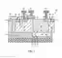
FIG. 1 is a cross-sectional side view of an isolation structure for a MOSFET, in accordance with some embodiments;
FIG. 2 to FIG. 8 are cross-sectional side views during a process to form the isolation structure for the MOSFET in FIG. 1, in accordance with some embodiments; and
FIG. 9 is a flowchart for a process for forming the isolation structure for the MOSFET in FIG. 1, in accordance with some embodiments.
DETAILED DESCRIPTION
The following disclosure provides many different embodiments, or examples, for implementing different features of the disclosure. Specific examples of components and arrangements are described below to simplify the present disclosure. These are examples and are not intended to be limiting.
In various embodiments, an isolation structure for a high voltage MOSFET is described. In some embodiments, high voltage MOSFETs, lower voltage devices, and the isolation structure described herein enable competitive advantage. For example, the isolation structure allows multiple capabilities to exist on the same substrate, thereby enabling new combined capabilities and a competitive advantage. In some embodiments, the isolation structure includes both a deep n-type doped well (“DNW”) layer and a deep p-type doped well (“DPW”) layer that are configured to mitigate or prevent electrical noise from the MOSFET from interfering with operation of other devices resident on the same substrate as the MOSFET device. Examples of other devices include RF and analog devices.
FIG. 1 is a cross-sectional side view of a MOSFET 300 having an isolation structure, in accordance with some embodiments. MOSFET 300 is a high voltage MOSFET formed on a p-type doped substrate (Psub) 302. MOSFET 300 includes a p-type doped well (PW) 304 and an n-type doped well (NW) 306. A source terminal 308 is capable of being electrically coupled with n-type doped source region 310. A drain terminal 312 is capable of being electrically coupled with n-type doped drain region 314. Between the source region 310 and the drain region 314 is a gate oxide 316 and conductive materials capable of being electrically coupled to a gate terminal 318. A deep n-type well (“DNW”) 320 and a deep p-type well (“DPW”) 322 function to electrically isolate the Psub 302. In some embodiments, the DPW 322 is formed by ion implantation. In some embodiments, the DPW 322 can be extended further to the left below the P-well 304 to enable a more conductive connection with the P-well 304. For example, a sidewall 322L of the DPW 322 is extended further to the left below the P-well 304. The DNW 320 is formed over the Psub 302 and the DPW 322 is formed in the DNW 320.
The DNW 320 is capable of being electrically coupled through a bias n-type doped well (“Bias NW”) 324, which is formed on the DNW 320 to a bias n-type doped region 326. The term “Bias” is intended to designate the function of the corresponding structure, in order to differentiate similar structures with different functions, and is not intended to limit the method of forming the identified bias structure. The bias n-type doped region 326 is capable of being electrically coupled with a DNW bias terminal 328. A voltage applied to the DNW bias terminal 328 passes through a conductive path to the DNW 320 in order to provide a voltage bias to the DNW 320. For example, a bias voltage applied to the DNW bias terminal 328 passes through the bias n-type doped region 326 and the Bias NW 324 to the DNW 320.
Analogous to the DNW 320, the DPW 322 is capable of being electrically coupled through a bias p-type doped well (“Bias PW”) 330, which is formed on the DPW 322 to a bias p-type doped region 332. The bias p-type doped region 332 is capable of being electrically coupled with a DPW bias terminal 334. A voltage applied to the DPW bias terminal 334 passes through a conductive path to the DPW 322 in order to provide a voltage bias to the DPW 322. For example, a bias voltage applied to the DPW bias terminal 334 passes through the bias p-type doped region 332 and the Bias PW 330 to the DPW 322.
A portion of the PW 304 beneath the gate oxide 316 is used as a channel region. The PW 304 is capable of being electrically coupled to a conductive bias voltage terminal 338. Shallow trench isolation (STI) structures 340A, 340B, and 340C are formed between the n-type doped regions 310, 314, 326, and corresponding p-type doped regions 332, 336. For example, the STI structure 340A is formed between the n-type doped region 326 and the p-type doped region 336. The STI structure 340B is formed between the p-type doped region 336 and the n-type doped region 310. The STI structure 340C is formed adjacent the n-type doped region 314. The STI structures 340A, 340B, and 340C serve to electrically isolate voltages applied to the terminals 308, 312, 318, 328, 334, 338 to power, control and bias the MOSFET 300. In some embodiments, the bias voltage terminal 338 is used to bias DPW 322.
The isolation structure associated with MOSFET 300 is superior to the structures in other approaches because the DNW 320 in combination with the DPW 322 greatly reduce electrical noise leaking into the Psub 302 that would otherwise interfere with lower voltage devices resident on the Psub 302. For example, in other approaches that do not have the DNW 320 and/or the DPW 322, the corresponding structure is susceptible to electrical noise from the high voltage MOSFET when the output of the MOSFET is transitioning.
Three dimensions, X, Y and Z are shown in FIG. 1. Dimension X represents a thickness of the DPW 322. Dimension Y represents a thickness of the DNW 320 with reference to DPW 322. Dimension Z represents a combined thickness of dimension X and dimension Y. In some embodiments, dimension X is between 100 nanometers (nm) and 600 nm. Dimension Y is between 100 nm and 900 nm. Dimension Z is between 200 nm and 1,500 nm. In some embodiments, the selected thickness of dimension X depends on the voltages applied, i.e., dimension X is selected to thick enough to prevent voltage punch-through.
In some embodiments, the n-type doped regions 326, 310, and 314 are n+ type as illustratively shown in FIG. 1. In some embodiments, the p-type doped regions 336 and 332 are p+ type as illustratively shown in FIG. 1.
FIG. 2 is a cross-sectional side view 400 during a process to form an isolation structure for the MOSFET 300, in accordance with some embodiments. P-type dopants are introduced into a substrate to form Psub 302. The DNW 320 is formed in the Psub 302 in some embodiments. In other embodiments, the DNW 320 is formed over the Psub 302. In some embodiments, the DPW 322 is formed in the DNW 320. In some embodiments, the DPW 322 is formed by ion implantation, such as with Boron ions implanted at 300 kiloelectron volts (Key). In some other embodiments, boron difloride (BF2) ions are implanted at 100 Key to form the DPW 322. In other embodiments, the DPW 322 is formed by selective diffusion. In some embodiments, the ion concentration is between 1017 and 1019 ions per cubic centimeter. Subsequently, PW 304 and shallow trench isolation (STI) structure 340A are formed on the left side, and NW 306 and shallow trench isolation (STI) structure 340C are formed on the right side of the isolation structure of the MOSFET 300.
FIG. 3 is a cross-sectional side view 500 during a process to form an isolation structure for the MOSFET 300, in accordance with some alternative embodiments. In these alternative embodiments, p-type dopants are introduced into the substrate to form Psub 302. The DNW 320 is formed in the Psub 302 in some alternative embodiments. In other alternative embodiments, the DNW 320 is formed over the Psub 302. In some alternative embodiments, the DPW 322 is formed over the DNW 320. In some embodiments, the DPW 322 is formed in the DNW 320 by ion implantation, such as with Boron ions implanted at 300 kiloelectron volts (Key). In some other embodiments, boron difloride (BF2) ions are implanted at 100 Key to form the DPW 322. In other embodiments, the DPW 322 is formed by chemical vapor deposition (CVD). In some embodiments, the ion concentration is between 1017 and 1019 ions per cubic centimeter. Subsequently, the PW 304 and shallow trench isolation (STI) structure 340A are formed on the left side, and NW 306 and shallow trench isolation (STI) structure 340C are formed on the right side of the isolation structure of the MOSFET 300.
FIG. 3 depicts an alternative structure of the structure of FIG. 2. The following description is based on the structure of FIG. 2, and is also applicable to the structure of FIG. 3.
FIG. 4 is a cross-sectional side view 600 during a process to form an isolation structure for the MOSFET 300, in accordance with some embodiments. Following a CMOS process and building on the structure shown in FIG. 2, gate oxide 316 is deposited over the PW 304 and NW 306. In some embodiments, other dielectric materials are used in place of silicon dioxide for the gate oxide 316. A conductive layer 642, is deposited over the gate oxide 316. In some embodiments, the conductive layer 642 is polysilicon.
FIG. 5 is a cross-sectional side view 700 during a process to form an isolation structure for the MOSFET 300, in accordance with some embodiments. An n-type lightly doped drain/source (NLDD) region implant is used to form an N-LDD portion 744 of PW 304. N-LDD photoresist 746 is formed over the NW 306, the conductive layer 642, and the STI 340C to block the MOSFET drain.
FIG. 6 is a cross-sectional side view 800 during a process to form an isolation structure for the MOSFET 300, in accordance with some embodiments. An n-type ion implant of the source region 310 and the drain region 314 is performed. In some embodiments, the n-type ion implant is n+ type, as illustrated by “n+S/D implant” in FIG. 6. A photoresist 848 is formed over the NW 306 and the conductive layer 642 to block the MOSFET drain.
FIG. 7 is a cross-sectional side view 900 during a process to form an isolation structure for the MOSFET 300, in accordance with some embodiments. In some embodiments, a p-type counter dopant implant is introduced to a gap between photoresist 950 and photoresist 952 over a drain area of the NW 306, to form a p+ or P-LDD region 1054, as shown in FIG. 8.
FIG. 8 is a cross-sectional side view 1000 during a process to form an isolation structure for the MOSFET 300, in accordance with some embodiments. In some embodiments, silicide area 1056A is formed in source area 310, silicide area 1056B is formed in polysilicon 642, and silicide area 1056C is formed in drain area 314.
FIG. 9 is a flowchart 1100 for a process for forming an isolation structure for a MOSFET, such as MOSFET 300, in accordance with some embodiments. A p-type dopant is added to a semiconductor substrate in step 1160 to form Psub 302. A deep n-type well 320 is formed adjacent to the Psub 302 in step 1162. A deep p-type well 322 is formed in the deep n-type well 320 in step 1164. The deep p-type well 322 is separated from the Psub 302 by the deep n-type well 320. An n-type well 306 is formed over the deep p-type well 322 in step 1166. The drain terminal is later formed over the n-type well 306. A p-type well 304 is formed over the deep n-type well 320 in step 1168. The source terminal is later formed over the p-type well 304. The p-type well 304 is formed adjacent to the n-type well 306.
In some embodiments, a structure comprises a p-type substrate, a deep n-type well and a deep p-type well. The deep n-type well is adjacent to the p-type substrate and has a first conductive path to a first terminal. The deep p-type well is in the deep n-type well, is separated from the p-type substrate by the deep n-type well, and has a second conductive path to a second terminal. A first n-type well is over the deep p-type well. A first p-type well is over the deep p-type well.
In some embodiments, a structure comprises a p-type substrate, a deep n-well, a deep p-well, a first n-type well, and a first p-type well. The deep n-well is over the p-type substrate. The deep p-well is in the deep n-well. The first n-type well is over the deep p-well. The first p-type well is over the deep p-well. A second n-type well is over the deep n-well.
In a method of some embodiments, a deep n-type well is formed adjacent a p-type substrate. A deep p-type well is in the deep n-type well, is separated from the p-type substrate by the deep n-type well. A first n-type well is formed over the deep p-type well. A first p-type well is formed over the deep p-type well. The first p-type well serves as a conductive path from the deep p-type well to a terminal. A portion of the deep p-type well in electrical connection with the first p-type well is determined based on conducitve connection between the deep p-type well and the first p-type well.
One of ordinary skill in the art will recognize the operations of method 1100 are merely examples and additional operations are includable, describe operations are removable and an order of operations are adjustable without deviating from the scope of method 1100.
It will be readily seen by one of ordinary skill in the art that the disclosed embodiments fulfill one or more of the advantages set forth above. After reading the foregoing specification, one of ordinary skill in the pertinent art will be able to affect various changes, substitutions of equivalents and various other embodiments as broadly disclosed herein. It is therefore intended that the protection granted hereon be limited only by the definition contained in the appended claims and equivalents thereof.
Claims
What is claimed is:1. A structure comprising:
a p-type substrate;
a deep n-type well adjacent to the p-type substrate and having a first conductive path to a first terminal;
a deep p-type well
in the deep n-type well,
separated from the p-type substrate by the deep n-type well, and
having a second conductive path to a second terminal;
a first n-type well over the deep p-type well; and
a first p-type well over the deep p-type well.
2. The structure of claim 1, wherein
a portion of the deep p-type well is not adjacent to the first n-type well.
3. The structure of claim 1, wherein
the first conductive path includes
a second n-type well;
an n-type doped region in the second n-type well; and
the first terminal; and
the first terminal is configured to bias the deep n-type well.
4. The structure of claim 1, wherein
the second conductive path includes
a second p-type well;
a p-type doped region in the second p-type well; and
the second terminal; and
the second terminal is configured to bias the deep p-type well.
5. The structure of claim 4, comprising
a third terminal configured to bias the deep p-type well.
6. The structure of claim 1 comprising
a source terminal of a transistor and a drain terminal of the transistor,
wherein
the drain terminal is over the first n-type well; and
the source terminal is over the first p-type well.
7. A structure comprises:
a p-type substrate;
a deep n-well over the p-type substrate;
a deep p-well in the deep n-well;
a first n-type well over the deep p-well;
a first p-type well over the deep p-well; and
a second n-type well over the deep n-well.
8. The structure of claim 7, comprising
a conductive path through the second n-type well to the deep n-well.
9. The structure of claim 7, comprising
an n-type region; and
a terminal,
wherein
the n-type region and the terminal are electrically connected with the second n-type well and with the deep n-well.
10. The structure of claim 7, comprising
a second p-type well over the deep p-well.
11. The structure of claim 10, comprising
a conductive path through the second p-type well to the deep p-well.
12. The structure of claim 10, comprising
a p-type region
a terminal,
wherein
the p-type region and the terminal are electrically connected with the second p-type well and with the deep p-well.
13. The structure of claim 7, wherein
the first p-type well is over the deep n-well.
14. The structure of claim 7, wherein
a portion of the deep p-well is under the first p-type well, and is determined based on conducitve connection between the deep p-well and the first p-type well.
15. The structure of claim 7, wherein
the deep n-well comprises a thickness thicker than a thickness of the deep p-well; and
the thickness of the deep n-well is selected based on a voltage punch-through.
16. The structure of claim 7 comprising
a source terminal of a transistor and a drain terminal of the transistor,
wherein
the drain terminal is over the first n-type well; and
the source terminal is over the first p-type well.
17. A method comprising:
forming a deep n-type well adjacent a p-type substrate;
forming a deep p-type well in the deep n-type well, the deep p-type well separated from the p-type substrate by the deep n-type well;
forming a first n-type well over the deep p-type well; and
forming a first p-type well over the deep p-type well,
wherein
the first p-type well serves as a conductive path from the deep p-type well to a terminal; and
a portion of the deep p-type well in electrical connection with the first p-type well is determined based on conducitve connection between the deep p-type well and the first p-type well.
18. The method of claim 17, wherein
the deep p-type well is formed by ion implantation of boron or of boron diflouride.
19. The method of claim 17, wherein
the deep p-type well is formed by ion implantation of boron or of boron diflouride with a voltage in the kiloelectron volts.
20. The method of claim 17, wherein
a thickness of the deep n-well is greater than a thickness of the deep p-well; and
the thickness of the deep n-well is selected based on a voltage punch-through.
Images & Drawings included:


Sources:
- United States Patent and Trademark Office - verify current appl. status at the USPTO↗
Similar patent applications:
- » 20100255233
Composition for plug in base-isolated structure, plug for base-isolated structure and base-isolated structure - » 20220302190
Semiconductor structure including isolation structure and method for forming isolation structure - » 20190115388
Image sensor with dual trench isolation structures at different isolation structure depths - » 20220037195
Method of forming semiconductor isolation structure and semiconductor isolation structure - » 20230052736
METHOD FOR MANUFACTURING SHALLOW TRENCH ISOLATION STRUCTURE, SHALLOW TRENCH ISOLATION STRUCTURE AND SEMICONDUCTOR STRUCTURE - » 20240290834
SEMICONDUCTOR DEVICE INCLUDING BACKSIDE ISOLATION STRUCTURE AND PLACEHOLDER ISOLATION STRUCTURE - » 20200006117
Method for fabricating semiconductor device comprising a deep trench isolation structure and a trap rich isolation structure in a substrate - » 20190206720
Semiconductor device comprising a deep trench isolation structure and a trap rich isolation structure in a substrate and a method of making the same - » 20210296159
Semiconductor device comprising a deep trench isolation structure and a trap rich isolation structure in a substrate and a method of making the same - » 20080032482
Isolation structures and methods of fabricating isolation structures
Recent applications in this class:
- » 20240120371 2024-04-11
CIRCUITS HAVING ENHANCED ELECTRICAL ISOLATION - » 20240014260 2024-01-11
HIGH VOLTAGE RESISTOR WITH HIGH VOLTAGE JUNCTION TERMINATION - » 20230299133 2023-09-21
ISOLATION STRUCTURE FOR ACTIVE DEVICES - » 20230062444 2023-03-02
Semiconductor structure and method for guarding a low voltage surface region from a high voltage surface region - » 20230017218 2023-01-19
SEMICONDUCTOR DEVICE AND MANUFACTURING METHOD OF SEMICONDUCTOR DEVICE - » 20220320272 2022-10-06
SEMICONDUCTOR DEVICE AND METHOD FOR MANUFACTURING SEMICONDUCTOR DEVICE - » 20220199769 2022-06-23
Method for fabricating semiconductor device with P-N junction isolation structure - » 20220199768 2022-06-23
Semiconductor device with P-N junction isolation structure and method for fabricating the same - » 20210367030 2021-11-25
Device isolator with reduced parasitic capacitance - » 20210043726 2021-02-11
Isolation structure for active devices
Recent applications for this Assignee:
- » 20250294856 2025-09-18
STACKED TRANSISTORS AND METHOD OF FORMING THE SAME - » 20250294853 2025-09-18
SEMICONDUCTOR DEVICE STRUCTURE WITH METAL GATE STACK - » 20250294838 2025-09-18
SEMICONDUCTOR DEVICES AND METHODS OF FABRICATING THE SAME - » 20250294819 2025-09-18
METHOD OF MANUFACTURING A SEMICONDUCTOR DEVICE AND A SEMICONDUCTOR DEVICE - » 20250294814 2025-09-18
SEMICONDUCTOR DEVICE WITH OXIDE-BASED SEMICONDUCTOR CHANNEL - » 20250294731 2025-09-18
NOVEL METAL FUSE STRUCTURE BY VIA LANDING - » 20250293173 2025-09-18
CHIP PACKAGE AND METHOD OF FORMING THE SAME - » 20250293148 2025-09-18
DECOUPLING CAPACITORS WITH BACK SIDE POWER RAILS - » 20250293106 2025-09-18
SEMICONDUCTOR PACKAGE - » 20250293104 2025-09-18
PACKAGE ASSEMBLY AND MANUFACTURING METHOD THEREOF