Method of manufacturing electronic package module
US20150035201A1
2015-02-05
13/955,149
2013-07-31
✅ Patent granted
US 9,814,166 B2
2017-11-07
-
-
Savitr Mulpuri
Foley & Lardner LLP | Cliff Z. Liu
2036-01-04
Abstract:
A method of manufacturing electronic package module is provided. The method provides selective molding by attaching tapes on the circuit substrate on which electric components are mounted thereon, forming molding compound to cover the circuit substrate, and removing tapes along with the molding compound thereon.
Inventors:
- TSUNG-JUNG CHENG 5 🇹🇼 NANTOU COUNTY, Taiwan
- JEN-CHUN CHEN 5 🇹🇼 NANTOU COUNTY, Taiwan
- CHIA-CHENG LIU 2 🇹🇼 NANTOU COUNTY, Taiwan
Assignee:
- Universal Scientific Industrial (Shanghai) Co., Ltd. 93 🇨🇳 Shanghai, China
Applicant:
Interested in similar patents?
Get notified when new applications in this technology area are published.
Classification:
H05K13/046 » CPC main
Apparatus or processes specially adapted for manufacturing or adjusting assemblages of electric components; Mounting of components, e.g. of leadless components Surface mounting
H05K13/046 » CPC main
Apparatus or processes specially adapted for manufacturing or adjusting assemblages of electric components; Mounting of components, e.g. of leadless components Surface mounting
H05K13/04 IPC
Apparatus or processes specially adapted for manufacturing or adjusting assemblages of electric components Mounting of components, e.g. of leadless components
H05K13/04 IPC
Apparatus or processes specially adapted for manufacturing or adjusting assemblages of electric components Mounting of components, e.g. of leadless components
H01L23/3114 » CPC further
Details of semiconductor or other solid state devices; Encapsulations, e.g. encapsulating layers, coatings, e.g. for protection characterised by the arrangement or shape the device being completely enclosed the device being a chip scale package, e.g. CSP
H01L24/02 » CPC further
Arrangements for connecting or disconnecting semiconductor or solid-state bodies; Methods or apparatus related thereto; Means for bonding being attached to, or being formed on, the surface to be connected, e.g. chip-to-package, die-attach, "first-level" interconnects; Manufacturing methods related thereto Bonding areas ; Manufacturing methods related thereto
H05K9/0024 » CPC main
Screening of apparatus or components against electric or magnetic fields; Casings with localised screening of components mounted on printed circuit boards [PCB] Shield cases mounted on a PCB, e.g. cans or caps or conformal shields
H05K9/0024 » CPC main
Screening of apparatus or components against electric or magnetic fields; Casings with localised screening of components mounted on printed circuit boards [PCB] Shield cases mounted on a PCB, e.g. cans or caps or conformal shields
H05K9/00 IPC
Screening of apparatus or components against electric or magnetic fields
H05K9/00 IPC
Screening of apparatus or components against electric or magnetic fields
H01L27/146 IPC
Devices consisting of a plurality of semiconductor or other solid-state components formed in or on a common substrate including semiconductor components sensitive to infra-red radiation, light, electromagnetic radiation of shorter wavelength or corpuscular radiation and specially adapted either for the conversion of the energy of such radiation into electrical energy or for the control of electrical energy by such radiation; Devices controlled by radiation Imager structures
H01L27/14618 » CPC further
Devices consisting of a plurality of semiconductor or other solid-state components formed in or on a common substrate including semiconductor components sensitive to infra-red radiation, light, electromagnetic radiation of shorter wavelength or corpuscular radiation and specially adapted either for the conversion of the energy of such radiation into electrical energy or for the control of electrical energy by such radiation; Devices controlled by radiation; Imager structures; Structural or functional details thereof Containers
H05K3/288 » CPC further
Apparatus or processes for manufacturing printed circuits; Secondary treatment of printed circuits; Applying non-metallic protective coatings Removal of non-metallic coatings, e.g. for repairing
H05K3/288 » CPC further
Apparatus or processes for manufacturing printed circuits; Secondary treatment of printed circuits; Applying non-metallic protective coatings Removal of non-metallic coatings, e.g. for repairing
H01L2924/0002 » CPC further
Indexing scheme for arrangements or methods for connecting or disconnecting semiconductor or solid-state bodies as covered by; Technical content checked by a classifier Not covered by any one of groups , and
H05K1/0224 » CPC further
Printed circuits; Details; Electrical arrangements not otherwise provided for; Reduction of cross-talk, noise or electromagnetic interference by printed shielding conductors, ground planes or power plane Patterned shielding planes, ground planes or power planes
H05K1/0224 » CPC further
Printed circuits; Details; Electrical arrangements not otherwise provided for; Reduction of cross-talk, noise or electromagnetic interference by printed shielding conductors, ground planes or power plane Patterned shielding planes, ground planes or power planes
H05K2203/0191 » CPC further
Indexing scheme relating to apparatus or processes for manufacturing printed circuits covered by; Tools for processing; Objects used during processing Using tape or non-metallic foil in a process, e.g. during filling of a hole with conductive paste
H05K2203/0191 » CPC further
Indexing scheme relating to apparatus or processes for manufacturing printed circuits covered by; Tools for processing; Objects used during processing Using tape or non-metallic foil in a process, e.g. during filling of a hole with conductive paste
H05K2203/107 » CPC further
Indexing scheme relating to apparatus or processes for manufacturing printed circuits covered by; Using electric, magnetic and electromagnetic fields; Using laser light Using laser light
H05K2203/107 » CPC further
Indexing scheme relating to apparatus or processes for manufacturing printed circuits covered by; Using electric, magnetic and electromagnetic fields; Using laser light Using laser light
H05K2203/1105 » CPC further
Indexing scheme relating to apparatus or processes for manufacturing printed circuits covered by; Treatments characterised by their effect, e.g. heating, cooling, roughening Heating or thermal processing not related to soldering, firing, curing or laminating, e.g. for shaping the substrate or during finish plating
H01L21/56 » CPC further
Processes or apparatus adapted for the manufacture or treatment of semiconductor or solid state devices or of parts thereof; Manufacture or treatment of semiconductor devices or of parts thereof the devices having at least one potential-jump barrier or surface barrier, e.g. PN junction, depletion layer or carrier concentration layer; Assembly of semiconductor devices using processes or apparatus not provided for in a single one of the subgroups - , e.g. sealing of a cap to a base of a container Encapsulations, e.g. encapsulation layers, coatings
H01L23/00 IPC
Details of semiconductor or other solid state devices
H01L23/31 IPC
Details of semiconductor or other solid state devices; Encapsulations, e.g. encapsulating layers, coatings, e.g. for protection characterised by the arrangement or shape
H01L23/552 » CPC further
Details of semiconductor or other solid state devices Protection against radiation, e.g. light or electromagnetic waves
H05K3/28 IPC
Apparatus or processes for manufacturing printed circuits; Secondary treatment of printed circuits Applying non-metallic protective coatings
H05K3/28 IPC
Apparatus or processes for manufacturing printed circuits; Secondary treatment of printed circuits Applying non-metallic protective coatings
H05K1/02 IPC
Printed circuits Details
H05K1/02 IPC
Printed circuits Details
H05K2201/0707 » CPC further
Indexing scheme relating to printed circuits covered by; Electric details Shielding
H05K2201/0707 » CPC further
Indexing scheme relating to printed circuits covered by; Electric details Shielding
H05K2201/1056 » CPC further
Indexing scheme relating to printed circuits covered by; Details of components or other objects attached to or integrated in a printed circuit board; Details of mounted components Metal over component, i.e. metal plate over component mounted on or embedded in PCB
H05K2201/1056 » CPC further
Indexing scheme relating to printed circuits covered by; Details of components or other objects attached to or integrated in a printed circuit board; Details of mounted components Metal over component, i.e. metal plate over component mounted on or embedded in PCB
Description
BACKGROUND OF THE INVENTION
1. Field of the Invention
The instant disclosure relates to a method of manufacturing electronic package module; in particular, to a method of manufacturing electronic package module providing selective molding.
2. Description of Related Art
Many electronic package modules typically include a circuit substrate and a plurality of electronic components, such as chip packages or passive components, mounted on the circuit substrate. Moreover, majority of the electronic package modules typically include molding compound to encapsulate the electronic components for protection.
However, certain electronic components, especially optical components such as CMOS image sensor (CIS), charge-coupled device (CCD), similar types of image sensors, light emitting diodes (LEDs), or similar types of light emitting elements, are not preferred to be encapsulated with molding which can impact normal operations of the circuit.
To address the above issues, the inventor strives via associated experience and research to present the instant disclosure, which can effectively improve the limitation described above.
SUMMARY OF THE INVENTION
The object of the instant disclosure is to provide a method of manufacturing electronic package module which can selective mold over electronic components.
In order to achieve the aforementioned objects, according to an embodiment of the instant disclosure, the method of manufacturing electronic package module includes the steps of providing a circuit substrate including: a mountable surface, at least one ground pad and at least one patterned predetermined region. The patterned predetermined region is defined on the mountable surface, and the ground pad is proximate to the predetermined region. At least one electronic component is mounted on at least one portion of the mountable surface other than the predetermined region. At least one tape is attached in the patterned predetermined region conforming to the shape of the patterned predetermined region. A molding is formed over the mountable surface. The molding covers the tape and the at least one electronic component. The molding formed on the patterned predetermined region is removed, and then the tape is removed.
According to one preferred embodiment of the instant disclosure, in the step of removing the molding includes the step of laser-scribing at least one groove correspondingly to the patterned predetermined region on the molding above the ground pad.
According to another preferred embodiment of the instant disclosure, in the step of removing the molding includes the step of trimming the molding above the predetermined region with laser-scribing.
According to another preferred embodiment of the instant disclosure, in the step of removing the tape on the predetermine region, heat is provided to facilitate the removal of the tape.
According to another preferred embodiment of the instant disclosure, the tape is an ultraviolet tape and in the step of removing the tape from the predetermined region, the tape is radiated by ultraviolet rays to remove the tape.
By applying the instant disclosure, selective molding is provided only to portion or portions which need molding and metal coating formed thereon. The method can be applied without opening new molding or performing complex steps while providing electromagnetic disturbance (EMI) shielding and keeping optical components from being encapsulated which can affect normal operations.
In order to further understand the instant disclosure, the following embodiments and illustrations are provided. However, the detailed description and drawings are merely illustrative of the disclosure, rather than limiting the scope being defined by the appended claims and equivalents thereof.
BRIEF DESCRIPTION OF THE DRAWINGS
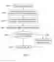
FIG. 1 is a schematic flow diagram of a method of manufacturing electronic package module in accordance with an embodiment of the instant disclosure;
FIG. 2A to 21 are schematic diagrams illustrating the method of manufacturing electronic package module in accordance with an embodiment of the instant disclosure; and
FIG. 3 is a schematic diagram illustrating the method of manufacturing electronic package module being applied on an exemplary predetermined region in accordance with another embodiment of the instant disclosure.
DETAILED DESCRIPTION OF THE PREFERRED EMBODIMENTS
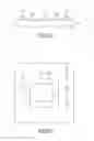
Please refer to FIG. 1 as a schematic flow diagram of a method of manufacturing electronic package module in accordance with an embodiment of the instant disclosure. Please refer to FIGS. 2A to 2H in conjunction with FIG. 1. FIGS. 2A, 2C, 2E, and 2G are cross-section views of the electronic package module illustrating the method of manufacturing electronic package module in accordance with an embodiment of the instant disclosure. FIGS. 2B, 2D, 2F, and 2H are overhead views of the electronic package module illustrating the method of manufacturing electronic package module in accordance with an embodiment of the instant disclosure.
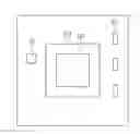
Please refer to FIGS. 1, 2A, and 2B as an embodiment of the method. A circuit substrate 11 is provided (Step S101). The circuit substrate 11 has a mountable surface 12, at least one predetermined region 101 defined on the mountable surface 12, and at least one ground pad 111. The ground pad 111 surrounds the periphery of the predetermined region 101 as an example of the instant embodiment, but not limited herein. The ground pad 111 can be of various sizes, shapes, and dimensions depending on the preference of the design. Moreover, electronic components 21 are mounted on any portions of the mountable surface 12 other than the predetermined region 101 (Step S102). The mountable surface can use surface mount technology (SMT) to mount non-optical electronic components 21 such as discrete passive components, but not limited to examples provided herein.
Please refer to FIG. 3. The predetermined region 102 in the instant embodiment can be a patterned predetermined region 102 as shown in FIG. 3. In other words, the shape of the predetermined region 102 is not limited to the examples of the embodiments provided herein. Thus, the quantity, surface area, size and shape of the predetermined region are not limited. The predetermined region facilitates access to positions of electronic components, such as CMOS, CCD, or other types of image sensors, or light emitting components (LEDs, etc), that may have been covered by molding 15 post regular manufacturing processes.
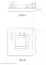
Please refer to FIGS. 1, 2A, 2B, 2C, and 2D. At least one piece of tape is attached on the circuit substrate 11 in the predetermined region 101 (Step 103). Thereafter, molding 15 is formed over the entire circuit substrate 11 (Step 104). The molding 15 encapsulates both the tape 13 and circuit substrate 11, and further encapsulates electronic components 21 and ground pads 111 which are mounted on portions of the circuit substrate 11 besides the predetermined region 101. Specifically, the molding 15 is formed by transfer molding or compression molding. The tape 13 can be attached to partially cover the ground pads 111 or not cover the ground pads 111 nearby, but is not limited herein.
Please refer to FIGS. 1, 2E, and 2F. After the molding 15 is formed, at least one groove is formed at portions of the molding 15 surrounding the patterned predetermined region 101 (Step 105). In other words, the groove is cut along the ground pad 111. The ground pad 111 is a metal layer and the molding 15 is commonly made of resins. As a result, laser cutting is ceased at the ground pad 111 due to the difference in the degree of laser absorption between the ground pad 111 and the molding 15 materials. As long as the molding 15 is cut and the circuit substrate 11 remains, the steps are not limited herein. For example, the groove can be formed on the molding 15 by routing.
Please refer to FIGS. 1, 2G, and 2H. Once the tape 13 is removed (Step S107), molding 15 only remains on portions of the circuit substrate 11 other than the predetermined region 101. Moreover, the tape 13 can be a thermal tape which releases adhesion upon heat, whereas the UV tape releases adhesion upon UV light, but is not limited the examples provided herein. In one embodiment, the tape 13 can be thin film having a thickness approximately 20-50 microns (micrometers, μm) as an example.
Please refer to FIG. 1 as the flow chart. In another embodiment of the instant disclosure, the tape 13 can be a thick film having a thickness of 0.2 millimeter (mm). After at least one groove is laser-scribed onto the molding 15 according to the patterned predetermined region (Step S105), further trimming can be done on the molding 15 according to the patterned predetermined region (the molding 15 above the tape 13) (Step S106). In other words, the molding 15 on the patterned predetermined region 101 is removed, and then the tape 13 is removed. Thus, molding 15 only remains on portions of the circuit substrate 11 other than the predetermined region 101.
In another embodiment of the instant disclosure, once tape is removed, an electromagnetic shielding layer is formed over portions of the molding other than the predetermined region and is electrically connected to the ground pad. Then optical components are mounted in the predetermined region. In other embodiments, once the tape is removed, optical components can be first mounted in the predetermined region, then successively form the electromagnetic shielding layer over portions of the molding other than the predetermined region and then electrically connect to the ground pad. As shown in FIG. 1, the electromagnetic shielding layer 19 and the ground pad 111 remains electrically connected such that electromagnetic shielding is provided. The electromagnetic shielding layer can be formed by spray coating, electroless plating, or sputtering. The optical components are mounted on the predetermined region via method such as surface mount technology (SMT).
In summary, the instant disclosure provides a method of manufacturing electronic package module which facilitates selective molding. Selective molding is formed on the circuit substrate by attaching tape on the circuit substrate and traces, and then removing the tape along with the molding on the tape. Then a predetermined region is formed without molding thereon, and optical components not preferred to be molded are then mounted on the predetermined region. Thus, electromagnetic disturbance (EMI) is provided while preventing optical components from being encapsulated by molding, which affects normal operations.
The figures and descriptions supra set forth illustrated the preferred embodiments of the instant disclosure; however, the characteristics of the instant disclosure are by no means restricted thereto. All changes, alternations, combinations or modifications conveniently considered by those skilled in the art are deemed to be encompassed within the scope of the instant disclosure delineated by the following claims.
Claims
What is claimed is:1. A method of manufacturing electronic package module comprising the steps of:
providing a circuit substrate comprising:
a mountable surface;
at least one ground pad mounted on the mountable surface; and
at least one patterned predetermined region defined on the mountable surface;
mounting at least one electronic component on at least one portion of the mountable surface other than the predetermined region;
attaching at least one tape in the patterned predetermined region conforming to the shape of the patterned predetermined region;
forming a molding over the mountable surface, wherein the molding covers the tape and the at least one electronic component;
removing the molding formed on the patterned predetermined region; and
removing the tape.
2. The method of manufacturing electronic package module as recited in claim 1, wherein the ground pad is configured between the at least one electronic component and the predetermined region, and in the step of removing the molding further comprises the step of:
laser-scribing at least one groove correspondingly to the patterned predetermined region on the molding above the ground pad.
3. The method of manufacturing electronic package module as recited in claim 1, wherein in the step of removing the molding further comprises the step of:
trimming the molding above the predetermined region with laser-scribing.
4. The method of manufacturing electronic package module as recited in claim 1, wherein in the step of removing the tape, heat is provided to facilitate the removal of the tape.
5. The method of manufacturing electronic package module as recited in claim 1, wherein the tape is an ultraviolet tape.
6. The method of manufacturing electronic package module as recited in claim 4, wherein in the step of removing the tape, the tape is radiated by ultraviolet rays to remove the tape.
7. The method of manufacturing electronic package module as recited in claim 1, wherein after the step of removing the tape, the method further comprises the step of:
mounting at least one optical component in the predetermined region.
8. The method of manufacturing electronic package module as recited in claim 7 further comprising:
forming an electromagnetic shielding layer over the molding layer to electrically connected to the ground pad.
9. The method of manufacturing electronic package module as recited in claim 1, wherein after the step of removing the tape, the method further comprises the step of:
forming an electromagnetic shielding layer over the molding layer to electrically connected to the ground pad.
10. The method of manufacturing electronic package module as recited in claim 9 further comprising the step of:
mounting at least one optical component in the predetermined region.
Images & Drawings included:


Sources:
- United States Patent and Trademark Office - verify current appl. status at the USPTO↗
Similar patent applications:
- » 20190012588
Packaged electronic module and manufacturing method thereof - » 14459367
Method of manufacturing electronic package module and electronic package module manufactured by the same - » 20190205718
Packaged electronic module and manufacturing method thereof - » 20050150875
Package sealing method, manufacturing method of electronic device modules, sealing apparatus, and packaged product - » 20110303993
SEMICONDUCTOR SENSOR DEVICE, METHOD OF MANUFACTURING SEMICONDUCTOR SENSOR DEVICE, PACKAGE, METHOD OF MANUFACTURING PACKAGE, MODULE, METHOD OF MANUFACTURING MODULE, AND ELECTRONIC DEVICE - » 20140126161
Electronic package module and method of manufacturing the same - » 20220359374
Electronic module, manufacturing method thereof and electronic package having the same - » 20230386992
Electronic module, manufacturing method thereof and electronic package having the same - » 20200167624
System and method for manufacturing and assembling packaged electronic modules - » 20180130761
SEMICONDUCTOR PACKAGE, MANUFACTURING METHOD THEREOF, AND ELECTRONIC ELEMENT MODULE USING THE SAME
Recent applications in this class:
- » 20240381603 2024-11-14
PRE-ASSEMBLY WARPAGE PAIRING - » 20240244814 2024-07-18
METHOD FOR PERFORMING ONLINE PICK-AND-PLACE PATH OPTIMIZATION SIMULTANEOUSLY DURING THE PRODUCTION OF A SURFACE MOUNT MACHINE - » 20240121932 2024-04-11
SELF-EQUALIZING FRAME FOR THERMAL MANAGEMENT DEVICE PRELOAD - » 20220312658 2022-09-29
Printed circuit board and method for manufacturing the same - » 20220217879 2022-07-07
Electronic device and method for manufacturing the same - » 20210227735 2021-07-22
THERMOCOMPRESSION BONDING WITH PASSIVATED SILVER-BASED CONTACTING METAL - » 20210227734 2021-07-22
Thermocompression Bonding with Passivated Gold Contacting Metal - » 20210227733 2021-07-22
Thermocompression bonding with passivated copper-based contacting metal - » 20210227732 2021-07-22
Thermocompression Bonding with Passivated Tin-Based Contacting Metal - » 20210219475 2021-07-15
Thermocompression bonding with passivated nickel-based contacting metal
Recent applications for this Assignee:
- » 20240153920 2024-05-09
ELECTRONIC DEVICE - » 20230352368 2023-11-02
POWER MODULE PACKAGING STRUCTURE - » 20230236243 2023-07-27
Electrical property testing device of evaluation board - » 20220253585 2022-08-11
Excitation source planning method for electrical simulation and system thereof - » 20220103105 2022-03-31
Power detecting device and method thereof - » 20220103103 2022-03-31
Vehicle driving device and method thereof - » 20210226657 2021-07-22
Wireless switch control device and method - » 20210088616 2021-03-25
Ultra wideband dynamic positioning method and system thereof - » 20190387610 2019-12-19
SiP module and manufacturing method of the SiP module - » 20190385952 2019-12-19
Method of manufacturing SiP module based on double plastic-sealing and the SiP module