Memory cell layout for low current field-induced MRAM
US20150161316A1
2015-06-11
14/619,701
2015-02-11
✅ Patent granted
US 10,606,973 B2
2020-03-31
-
-
Yu-Hsi D Sun
McAndrews, Held & Malloy, Ltd.
2035-02-11
Abstract:
Embodiments of the present invention disclose an MRAM cell layout for 32 nm, 45 nm, and 65 nm CMOS process technology.
Assignee:
- III Holdings 1, LLC 196 🇺🇸 Wilmington, DE, United States
Applicant:
Interested in similar patents?
Get notified when new applications in this technology area are published.
Classification:
H01L27/222 » CPC further
Devices consisting of a plurality of semiconductor or other solid-state components formed in or on a common substrate including components using galvano-magnetic effects, e.g. Hall effects; using similar magnetic field effects Magnetic non-volatile memory structures, e.g. MRAM
H01L43/08 » CPC further
Devices using galvano-magnetic or similar magnetic effects; Processes or apparatus specially adapted for the manufacture or treatment thereof or of parts thereof Magnetic-field-controlled resistors
H01L27/22 IPC
Devices consisting of a plurality of semiconductor or other solid-state components formed in or on a common substrate including components using galvano-magnetic effects, e.g. Hall effects; using similar magnetic field effects
G11C11/16 » CPC further
Digital stores characterised by the use of particular electric or magnetic storage elements; Storage elements therefor using magnetic elements using elements in which the storage effect is based on magnetic spin effect
Description
This application is a division of U.S. patent application Ser. No. 13/369,267, filed Feb. 8, 2012, which claims the benefit of priority to U.S. Provisional Patent Application No. 61/440,630, filed Feb. 8, 2011, for which the entire specification and drawings of each application is incorporated here by reference.
FIELD
Embodiments of the invention relate to low power field-induced
MRAM cell layouts for 65 nm, 45 nm and 32 nm CMOS nodes.
BACKGROUND
In a field-induced magnetic random access memory (MRAM) a current-induced magnetic field generated around metal lines is used to write data into memory cells. Each memory cell stores a bit of data in a magnetic tunnel junction (MTJ). The MTJ is located at the intersection of two conductors in the form of a bit line and a word line. Normally, these lines are laid out perpendicular to each other. To write binary data (a “0” or a “1”) to a MTJ cell, enough current must flow simultaneously through the bit line and the word line associated with that particular cell for a certain amount of time. The sense in which the current flows in both metal lines sets the data value “0” or “1” in the cell.
In some embodiments of MRAM, data may be read from an MTJ through an access transistor connected to the MTJ, which forms part of the memory cell. This transistor is unique to the MTJ being addressed but parts of the transistor may be shared with transistors from neighboring cells.
SUMMARY
Embodiments of the present invention disclose an MRAM cell layout for 32 nm, 45 nm, and 65 nm CMOS process technology.
BRIEF DESCRIPTION OF THE DRAWINGS
FIG. 1 is a schematic drawing showing Level 1 of a MRAM cell layout, in accordance with one embodiment of the invention.
FIG. 2 is a schematic drawing showing Level 2 of the MRAM cell layout, in accordance with one embodiment of the invention.
FIG. 3 is a schematic drawing showing Level 3 of the MRAM cell layout, in accordance with one embodiment of the invention.
FIG. 4 is a schematic drawing showing a combination of Levels 1-3 of the MRAM cell layout.
FIG. 5 is a schematic drawing of a MRAM cell based on a MRAM cell layout, in accordance with one embodiment of the invention
DETAILED DESCRIPTION
In the following description, for purposes of explanation, numerous specific details are set forth in order to provide a thorough understanding of the invention. It will be apparent, however, to one skilled in the art that the invention can be practiced without these specific details. In other instances, structures and devices are shown in block diagram form only in order to avoid obscuring the invention.
Reference in this specification to “one embodiment” or “an embodiment” means that a particular feature, structure, or characteristic described in connection with the embodiment is included in at least one embodiment of the invention. The appearance of the phrase “in one embodiment” in various places in the specification are not necessarily all referring to the same embodiment, nor are separate or alternative embodiments mutually exclusive of other embodiments. Moreover, various features are described which may be exhibited by some embodiments and not by others. Similarly, various requirements are described which may be requirements for some embodiments but not other embodiments.
Although the following description contains many specifics for the purposes of illustration, anyone skilled in the art will appreciate that many variations and/or alterations to said details are within the scope of the present invention. Similarly, although many of the features of the present invention are described in terms of each other, or in conjunction with each other, one skilled in the art will appreciate that many of these features can be provided independently of other features. Accordingly, this description of the invention is set forth without any loss of generality to, and without imposing limitations upon, the invention.
Field-induced MRAM relies on a magnetic field generated around metal lines to switch the magnetization of a MTJ. In most embodiments each cell has two crossing metal lines for this purpose. These lines are the bit line and the word line, respectively. The MTJ is located at the intersection of these two lines and at least the bit line is in contact with the MTJ.
In some embodiments of MRAM, the memory cell also comprises an access transistor connected to the MTJ. The final cell size may be defined by the metal lines' pitch and/or by the access transistor size.
Embodiments of the present invention disclose different MRAM cell layouts, and MRAM structures (cell and devices) based on said cell layouts. Each MRAM cell layout is optimized for a given level of CMOS process technology.
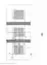
For clarity, the MRAM cell layout is divided into three levels. FIG. 1 shows the first level, FIG. 2 shows the second level, and FIG. 3 shows the third level. In the figures, M1 refers to a first level of metallization, M2 a second level, and M3 a third level.
FIG. 1, shows the layout for two cells at the CMOS transistor level, in plan view. Referring to FIG. 1, reference numeral 1 refers to a gate formed between contacts 2. The gate may be of poly-silicon, in one embodiment. Reference numeral 3 indicates an active area for the MRAM cell. Reference numeral 4 indicates the cell border. Reference numeral 5 indicates a metal 1 (M1) island. Reference numeral 6 indicates a via, referred to as via 1 Reference numeral 7 indicates a metal 1 line. Reference numeral 8 indicates a MTJ. Reference numeral 9 indicates a bottom electrode. Reference numerals 10 and 11 indicate a metal 2 line and a metal 3 line, respectively. The via 1 connects M2 and M1.
The second level depicted in FIG. 2 shows the MRAM cell layout from the M1 layer up to via 1, in plan view. Metal line 7 connecting the source is common for both transistors (left and right).
Referring to FIG. 3, the third level shows the magnetic region of the cell in plan view. The magnetic region includes layers: bottom electrode (9), MTJ (8), metal 2 (10) and metal 3 (11). The bottom electrode is also a seed layer for the MTJ-and connects the MTJ (8) to via 1 (6), which is the element connected to the access transistor through M2 (10) and Interface via (12). This electrode is shaped so that the MTJ (8) can be placed at the center of the cell, as shown in FIG. 3. In this way the magnetic interaction between neighboring cells is minimized, which is important to reduce variation in the switching field of the MTJ's.
FIG. 4 shows all levels of the cell combined.
FIG. 5 shows a side view of the MRAM cell, fabricated in accordance with the MRAM cell layout described above.
The final cell size depends on available CMOS manufacturing process capability. According to current manufacturing process a list of dimensions of the different elements of the cell and distances between some of those elements (as numbered in FIGS. 1 to 4) is provided in Table 1. The table covers MRAM cell layouts for CMOS nodes 65 nm, 45 nm and 32 nm.
| TABLE 1 |
| MRAM Cell Layout for 32 nm CMOS process technology |
| Size (nm) | ||
| Element | Description | 32 nm node cell |
| 1 | Poly-Si gate | 18 |
| 2 | Contact | 54 × 54 |
| 3 | Active area | 70 |
| width | ||
| 4 | Cell border | 180 × 140 |
| 5 | Metal 1 island | 67 × 84 |
| 6 | Via 1 | 54 × 54 |
| 7 | Metal 1 line | 58 |
| 8 | MTJ | 46 × 46 |
| 9 | Bottom | 95 × 66 |
| electrode | ||
| 10 | Metal 2 line | 58 |
| 12 | Interface via | 54 × 54 |
| 11 | Metal 3 line | 58 |
| d1 | 35 | |
| d2 | 114 | |
| d3 | 21 | |
| d4 | 21 | |
| d5 | 56 | |
| d6 | 114 | |
| d7 | 90 | |
| d8 | 57 | |
| TABLE 2 |
| MRAM Cell Layout for 45 nm CMOS process technology |
| Size (nm) | ||
| Element | Description | 45 nm node cell |
| 1 | Poly-Si gate | 25 |
| 2 | Contact | 70 × 70 |
| 3 | Active area | 80 |
| width | ||
| 4 | Cell border | 250 × 160 |
| 5 | Metal 1 island | 90 × 80 |
| 6 | Via 1 | 70 × 70 |
| 7 | Metal 1 line | 80 |
| 8 | MTJ | 65 × 65 |
| 9 | Bottom | 125 × 80 |
| electrode | ||
| 10 | Metal 2 line | 80 |
| 12 | Interface via | 70 × 70 |
| 11 | Metal 3 line | 80 |
| d1 | 40 | |
| d2 | 160 | |
| d3 | 35 | |
| d4 | 30 | |
| d5 | 80 | |
| d6 | 160 | |
| d7 | 125 | |
| d8 | 85 | |
| TABLE 3 |
| MRAM Cell Layout for 65 nm CMOS process technology |
| Size (nm) | |||
| Element | Description | 65 nm node cell | |
| 1 | Poly-Si gate | 35 | |
| 2 | Contact | 100 × 100 | |
| 3 | Active area | 110 | |
| width | |||
| 4 | Cell border | 350 × 220 | |
| 5 | Metal 1 island | 130 × 110 | |
| 6 | Via 1 | 100 × 100 | |
| 7 | Metal 1 line | 110 | |
| 8 | MTJ | 100 × 100 | |
| 9 | Bottom | 195 × 130 | |
| electrode | |||
| 10 | Metal 2 line | 120 | |
| 12 | Interface via | 100 × 100 | |
| 11 | Metal 3 line | 120 | |
| d1 | 55 | ||
| d2 | 235 | ||
| d3 | 50 | ||
| d4 | 50 | ||
| d5 | 110 | ||
| d6 | 230 | ||
| d7 | 175 | ||
| d8 | 110 | ||
In one embodiment, the MRAM cell layouts specified above may be stored in a format that supports data exchange of integrated circuit layouts. For example, the MRAM cell layouts may be stored in a Graphic. Database System (GDS) format such as in GDSII format stored a computer-readable medium. Examples of computer-readable media include but are not limited to recordable type media such as volatile and non-volatile memory devices, floppy and other removable disks, hard disk drives, optical disks (e.g., Compact Disk Read-Only Memory (CD ROMS), Digital Versatile Disks, (DVDs), etc.).
Although the present invention has been described with reference to specific example embodiments, it will be evident that various modifications and changes can be made to these embodiments without departing from the broader spirit of the invention.
Claims
1. A magnetic random access memory (MRAM) circuit comprising:
a cell;
a bottom electrode located within the cell; and
a magnetic tunnel junction (MTJ) located in the cell and above the bottom electrode;
wherein a ratio of a width of the bottom electrode to a width of the MJT is equal to or greater than approximately 1.9.
2. The MRAM circuit of claim 7, wherein the ratio is approximately 2.1 at a 32 nm complementary metal-oxide semiconductor (CMOS) process technology.
3. The MRAM circuit of claim 7, wherein the ratio is approximately 1.9 at a 45 nm CMOS process technology.
4. The MRAM circuit of claim 7, wherein the ratio is approximately 2.0 at a 65 nm CMOS process technology.
5. The MRAM circuit of claim 7, wherein the MTJ is located in a center of the cell.
6. The MRAM circuit of claim 11, wherein the bottom electrode is not centered at the center of the cell.
7. A magnetic random access memory (MRAM) circuit comprising:
a cell;
a bottom electrode located within the cell; and
a magnetic tunnel junction (MTJ) located in the cell and above the bottom electrode;
wherein a ratio of a width of the cell to a width of the MJT is equal to or greater than approximately 3.5.
8. The MRAM circuit of claim 13, wherein the ratio is approximately 3.9 at a 32 nm complementary metal-oxide semiconductor (CMOS) process technology.
9. The MRAM circuit of claim 13, wherein the ratio is approximately 3.8 at a 45 nm CMOS process technology.
10. The MRAM circuit of claim 13, wherein the ratio is approximately 3.5 at a 65 nm CMOS process technology.
11. The MRAM circuit of claim 13, wherein the MTJ is located in a center of the cell.
12. The MRAM circuit of claim 17, wherein the bottom electrode is not centered at the center of the cell.
13. A magnetic random access memory (MRAM) circuit comprising:
a cell;
a bottom electrode located within the cell; and
a magnetic tunnel junction (MTJ) located in the cell and above the bottom electrode;
wherein the MTJ is centered at the center of the cell and the bottom electrode is not centered at the center of the cell.
14. The MRAM circuit of claim 19, wherein a ratio of a width of the bottom electrode to a width of the MJT is equal to or greater than approximately 1.9.
15. The MRAM circuit of claim 20, wherein the ratio is approximately 2.1 at a 32 nm complementary metal-oxide semiconductor (CMOS) process technology.
16. The MRAM circuit of claim 20, wherein the ratio is approximately 1.9 at a 45 nm CMOS process technology.
17. The MRAM circuit of claim 20, wherein the ratio is approximately 2.0 at a 65 nm CMOS process technology.
Images & Drawings included:


Sources:
- United States Patent and Trademark Office - verify current appl. status at the USPTO↗
Similar patent applications:
- » 20200226315
Memory cell layout for low current field-induced MRAM - » 20220318474
Memory cell layout for low current field-induced MRAM
Recent applications in this class:
- » 20210011981 2021-01-14
Clock crossing interface for integrated circuit generation - » 20200372124 2020-11-26
System and method for ESL modeling of machine learning - » 20200257769 2020-08-13
Characterization of spatial correlation in integrated circuit development - » 20200242209 2020-07-30
Fill process optimization using feature scale modeling - » 20200184034 2020-06-11
Printed circuit board design - » 20200110852 2020-04-09
Predictive spatial digital design of experiment for advanced semiconductor process optimization and control - » 20200104444 2020-04-02
Multi-input logic circuitry - » 20200089834 2020-03-19
System and method for interactive datasheets - » 20200089833 2020-03-19
Methods for engineering integrated circuit design and development - » 20200074035 2020-03-05
Optimization of quantum circuits
Recent applications for this Assignee:
- » 20240373518 2024-11-07
TOOL FOR ANNEALING OF MAGNETIC STACKS - » 20240007687 2024-01-04
Method, device, and apparatus for pausing media content - » 20230251812 2023-08-10
Methods and Apparatus for Mesh Networking Using Wireless Devices - » 20220318474 2022-10-06
Memory cell layout for low current field-induced MRAM - » 20220179612 2022-06-09
Methods and apparatus for mesh networking using wireless devices - » 20220139221 2022-05-05
Intelligently providing user-specific transportation-related information - » 20220129231 2022-04-28
Wireless mesh-enabled system, host device, and method for use therewith - » 20220116666 2022-04-14
Methods and apparatus for pausing live service - » 20220104316 2022-03-31
Tool for annealing of magnetic stacks - » 20220027954 2022-01-27
System, Method and Computer Program Product for Extracting User Profiles and Habits Based on Speech Recognition and Calling History for Telephone System Advertising