Semiconductor package and fabrication method thereof
US20150243574A1
2015-08-27
14/256,496
2014-04-18
✅ Patent granted
US 9,343,401 B2
2016-05-17
-
-
Dao H Nguyen | Tram H. Nguyen
Mintz Levin Cohn Ferris Glovsky and Popeo, P.C. | Peter F. Corless | Steven M. Jensen
2034-05-08
Abstract:
A method for fabricating a semiconductor package is provided, which includes the steps of: providing a packaging substrate having a first surface with a plurality of bonding pads and an opposite second surface; disposing a plurality of passive elements on the first surface of the packaging substrate; disposing a semiconductor chip on the passive elements through an adhesive film; electrically connecting the semiconductor chip and the bonding pads through a plurality of bonding wires; and forming an encapsulant on the first surface of the packaging substrate for encapsulating the semiconductor chip, the passive elements and the bonding wires. By disposing the passive elements between the packaging substrate and the semiconductor chip, the invention saves space on the packaging substrate and increases the wiring flexibility. Further, since the bonding wires are not easy to come into contact with the passive elements, the invention prevents a short circuit from occurring.
Inventors:
- Hsin-Lung Chung 21 🇹🇼 Taichung, Taiwan
- Chia-Yang Chen 33 🇹🇼 Taichung, Taiwan
- Chi-Liang Shih 9 🇹🇼 Taichung, Taiwan
- Te-Fang Chu 6 🇹🇼 Taichung, Taiwan
- Sheng-Ming Yang 3 🇹🇼 Taichung, Taiwan
- Hung-Cheng Chen 3 🇹🇼 Taichung, Taiwan
Assignee:
- Siliconware Precision Industries Co., Ltd. 673 🇹🇼 Taichung, Taiwan
Applicant:
Interested in similar patents?
Get notified when new applications in this technology area are published.
Classification:
H01L23/3114 » CPC main
Details of semiconductor or other solid state devices; Encapsulations, e.g. encapsulating layers, coatings, e.g. for protection characterised by the arrangement or shape the device being completely enclosed the device being a chip scale package, e.g. CSP
H01L21/563 » CPC further
Processes or apparatus adapted for the manufacture or treatment of semiconductor or solid state devices or of parts thereof; Manufacture or treatment of semiconductor devices or of parts thereof the devices having at least one potential-jump barrier or surface barrier, e.g. PN junction, depletion layer or carrier concentration layer; Assembly of semiconductor devices using processes or apparatus not provided for in a single one of the subgroups - , e.g. sealing of a cap to a base of a container; Encapsulations, e.g. encapsulation layers, coatings Encapsulation of active face of flip-chip device, e.g. underfilling or underencapsulation of flip-chip, encapsulation preform on chip or mounting substrate
H01L21/56 IPC
Processes or apparatus adapted for the manufacture or treatment of semiconductor or solid state devices or of parts thereof; Manufacture or treatment of semiconductor devices or of parts thereof the devices having at least one potential-jump barrier or surface barrier, e.g. PN junction, depletion layer or carrier concentration layer; Assembly of semiconductor devices using processes or apparatus not provided for in a single one of the subgroups - , e.g. sealing of a cap to a base of a container Encapsulations, e.g. encapsulation layers, coatings
H01L23/49838 » CPC main
Details of semiconductor or other solid state devices; Arrangements for conducting electric current to or from the solid state body in operation, e.g. leads, terminal arrangements ; Selection of materials therefor consisting of soldered constructions; Leads, on insulating substrates, Geometry or layout
H01L24/92 » CPC further
Arrangements for connecting or disconnecting semiconductor or solid-state bodies; Methods or apparatus related thereto; Methods for connecting semiconductor or solid state bodies including different methods provided for in two or more of groups - Specific sequence of method steps
H01L2924/19103 » CPC further
Indexing scheme for arrangements or methods for connecting or disconnecting semiconductor or solid-state bodies as covered by; Details of hybrid assemblies other than the semiconductor or other solid state devices to be connected; Disposition of discrete passive components in a stacked assembly with the semiconductor or solid state device interposed between the semiconductor or solid-state device and the die mounting substrate, i.e. chip-on-passive
H01L23/3128 » CPC further
Details of semiconductor or other solid state devices; Encapsulations, e.g. encapsulating layers, coatings, e.g. for protection characterised by the arrangement or shape the device being completely enclosed a substrate forming part of the encapsulation the substrate having spherical bumps for external connection
H01L24/32 » CPC further
Arrangements for connecting or disconnecting semiconductor or solid-state bodies; Methods or apparatus related thereto; Means for bonding being attached to, or being formed on, the surface to be connected, e.g. chip-to-package, die-attach, "first-level" interconnects; Manufacturing methods related thereto; Layer connectors, e.g. plate connectors, solder or adhesive layers; Manufacturing methods related thereto; Structure, shape, material or disposition of the layer connectors after the connecting process of an individual layer connector
H01L24/46 » CPC further
Arrangements for connecting or disconnecting semiconductor or solid-state bodies; Methods or apparatus related thereto; Means for bonding being attached to, or being formed on, the surface to be connected, e.g. chip-to-package, die-attach, "first-level" interconnects; Manufacturing methods related thereto; Wire connectors; Manufacturing methods related thereto; Structure, shape, material or disposition of the wire connectors prior to the connecting process of a plurality of wire connectors
H01L24/83 » CPC further
Arrangements for connecting or disconnecting semiconductor or solid-state bodies; Methods or apparatus related thereto; Methods for connecting semiconductor or other solid state bodies using means for bonding being attached to, or being formed on, the surface to be connected using a layer connector
H01L24/27 » CPC further
Arrangements for connecting or disconnecting semiconductor or solid-state bodies; Methods or apparatus related thereto; Means for bonding being attached to, or being formed on, the surface to be connected, e.g. chip-to-package, die-attach, "first-level" interconnects; Manufacturing methods related thereto; Layer connectors, e.g. plate connectors, solder or adhesive layers; Manufacturing methods related thereto Manufacturing methods
H01L24/29 » CPC further
Arrangements for connecting or disconnecting semiconductor or solid-state bodies; Methods or apparatus related thereto; Means for bonding being attached to, or being formed on, the surface to be connected, e.g. chip-to-package, die-attach, "first-level" interconnects; Manufacturing methods related thereto; Layer connectors, e.g. plate connectors, solder or adhesive layers; Manufacturing methods related thereto; Structure, shape, material or disposition of the layer connectors prior to the connecting process of an individual layer connector
H01L24/48 » CPC further
Arrangements for connecting or disconnecting semiconductor or solid-state bodies; Methods or apparatus related thereto; Means for bonding being attached to, or being formed on, the surface to be connected, e.g. chip-to-package, die-attach, "first-level" interconnects; Manufacturing methods related thereto; Wire connectors; Manufacturing methods related thereto; Structure, shape, material or disposition of the wire connectors after the connecting process of an individual wire connector
H01L24/49 » CPC further
Arrangements for connecting or disconnecting semiconductor or solid-state bodies; Methods or apparatus related thereto; Means for bonding being attached to, or being formed on, the surface to be connected, e.g. chip-to-package, die-attach, "first-level" interconnects; Manufacturing methods related thereto; Wire connectors; Manufacturing methods related thereto; Structure, shape, material or disposition of the wire connectors after the connecting process of a plurality of wire connectors
H01L24/73 » CPC further
Arrangements for connecting or disconnecting semiconductor or solid-state bodies; Methods or apparatus related thereto Means for bonding being of different types provided for in two or more of groups , , , , , , ,
H01L2224/27436 » CPC further
Indexing scheme for arrangements for connecting or disconnecting semiconductor or solid-state bodies and methods related thereto as covered by; Means for bonding being attached to, or being formed on, the surface to be connected, e.g. chip-to-package, die-attach, "first-level" interconnects; Manufacturing methods related thereto; Layer connectors, e.g. plate connectors, solder or adhesive layers; Manufacturing methods related thereto; Manufacturing methods by blanket deposition of the material of the layer connector in solid form Lamination of a preform, e.g. foil, sheet or layer
H01L2224/73265 » CPC further
Indexing scheme for arrangements for connecting or disconnecting semiconductor or solid-state bodies and methods related thereto as covered by; Means for bonding being of different types provided for in two or more of groups; Location after the connecting process on different surfaces Layer and wire connectors
H01L2224/83191 » CPC further
Indexing scheme for arrangements for connecting or disconnecting semiconductor or solid-state bodies and methods related thereto as covered by; Methods for connecting semiconductor or other solid state bodies using means for bonding being attached to, or being formed on, the surface to be connected using a layer connector; Arrangement of the layer connectors prior to mounting wherein the layer connectors are disposed only on the semiconductor or solid-state body
H01L2224/92247 » CPC further
Indexing scheme for arrangements for connecting or disconnecting semiconductor or solid-state bodies and methods related thereto as covered by; Methods for connecting semiconductor or solid state bodies including different methods provided for in two or more of groups - ; Specific sequence of method steps; Connecting different surfaces of the semiconductor or solid-state body with connectors of different types; Sequential connecting processes the first connecting process involving a layer connector the second connecting process involving a wire connector
H01L2924/00014 » CPC further
Indexing scheme for arrangements or methods for connecting or disconnecting semiconductor or solid-state bodies as covered by; Technical content checked by a classifier the subject-matter covered by the group, the symbol of which is combined with the symbol of this group, being disclosed without further technical details
H01L2924/15311 » CPC further
Indexing scheme for arrangements or methods for connecting or disconnecting semiconductor or solid-state bodies as covered by; Details of package parts other than the semiconductor or other solid state devices to be connected; Die mounting substrate; Connection portion the connection portion being formed only on the surface of the substrate opposite to the die mounting surface being a ball array, e.g. BGA
H01L2924/181 » CPC further
Indexing scheme for arrangements or methods for connecting or disconnecting semiconductor or solid-state bodies as covered by; Details of package parts other than the semiconductor or other solid state devices to be connected Encapsulation
H01L2924/19105 » CPC further
Indexing scheme for arrangements or methods for connecting or disconnecting semiconductor or solid-state bodies as covered by; Details of hybrid assemblies other than the semiconductor or other solid state devices to be connected; Disposition of discrete passive components in a side-by-side arrangement on a common die mounting substrate
H01L29/04 IPC
Semiconductor devices adapted for rectifying, amplifying, oscillating or switching, or capacitors or resistors with at least one potential-jump barrier or surface barrier, e.g. PN junction depletion layer or carrier concentration layer; Details of semiconductor bodies or of electrodes thereof; Multistep manufacturing processes therefor; Semiconductor bodies ; Multistep manufacturing processes therefor characterised by their crystalline structure, e.g. polycrystalline, cubic or particular orientation of crystalline planes
H01L29/10 IPC
Semiconductor devices adapted for rectifying, amplifying, oscillating or switching, or capacitors or resistors with at least one potential-jump barrier or surface barrier, e.g. PN junction depletion layer or carrier concentration layer; Details of semiconductor bodies or of electrodes thereof; Multistep manufacturing processes therefor; Semiconductor bodies ; Multistep manufacturing processes therefor characterised by their shape; characterised by the shapes, relative sizes, or dispositions of the semiconductor regions ; characterised by the concentration or distribution of impurities within semiconductor regions with semiconductor regions connected to an electrode not carrying current to be rectified, amplified or switched and such electrode being part of a semiconductor device which comprises three or more electrodes
H01L31/00 IPC
Semiconductor devices sensitive to infra-red radiation, light, electromagnetic radiation of shorter wavelength or corpuscular radiation and specially adapted either for the conversion of the energy of such radiation into electrical energy or for the control of electrical energy by such radiation; Processes or apparatus specially adapted for the manufacture or treatment thereof or of parts thereof; Details thereof
H01L23/498 IPC
Details of semiconductor or other solid state devices; Arrangements for conducting electric current to or from the solid state body in operation, e.g. leads, terminal arrangements ; Selection of materials therefor consisting of soldered constructions Leads, on insulating substrates,
H01L23/31 IPC
Details of semiconductor or other solid state devices; Encapsulations, e.g. encapsulating layers, coatings, e.g. for protection characterised by the arrangement or shape
H01L23/00 IPC
Details of semiconductor or other solid state devices
Description
BACKGROUND OF THE INVENTION
1. Field of the Invention
The present invention relates to semiconductor packages and fabrication methods thereof, and more particularly, to a semiconductor package having passive elements and a fabrication method thereof.
2. Description of Related Art
The development of electronic products having small size and high performance requires IC elements having high memory capacities, high frequencies and low voltages. Further, the development of IC elements having high memory capacities, high frequencies and low voltages depends on the integration degree of electronic circuits and electronic elements of the IC elements and the density of I/O connectors used for signal transmission.
Currently, BGA type semiconductor devices capable of accommodating a large number of passive elements, such as capacitors, resistors, inductors and oscillators, have become a mainstream.
In some semiconductor application devices, such as communication or high-frequency semiconductor devices, semiconductor chips need to be electrically connected to passive elements, such as resistors, inductors, capacitors and oscillators, so as to obtain certain electric current characteristics or send certain signals.
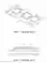
FIG. 1 is a schematic perspective view of a conventional BGA type semiconductor device. Referring to FIG. 1, a plurality of passive elements 11 and a plurality of semiconductor chips 12 are disposed on a surface of a substrate 10. To facilitate electrical connection between the semiconductor chips 12 and bonding fingers (not shown) of the substrate 10, the passive elements 11 are generally positioned at corners of the substrate 10 or outside chip mounting areas of the substrate 10. However, the limited positions of the passive elements 11 reduce the wiring flexibility of the substrate 10 and the limited positions of the boning fingers restrict the number of the passive elements 11 that can be disposed on the substrate 10, thereby hindering the development of highly integrated semiconductor devices. On the other hand, if the surface area of the substrate 10 is increased to accommodate a large number of passive elements 11 and semiconductor chips 12, the size of the final package will be increased. As such, it cannot meet the trend of miniaturization.
Accordingly, another conventional BGA type semiconductor device is provided. Referring to FIG. 2, a plurality of passive elements 22 are disposed between a semiconductor chip 23 and bonding fingers of the substrate. However, as the number of I/O connectors in a unit area of the semiconductor device increases, the number of bonding wires 21 also increases. Generally, the height of the passive elements 22 (e.g. 0.8 mm) is higher than the height of the semiconductor chip 23 (e.g., 0.55 mm) Therefore, to prevent the bonding wires 21 from coming into contact with the passive elements 22, the bonding wires must be positioned high above the passive elements 22, thus increasing the bonding difficulty and processing complexity. Also, wire loops of the bonding wires 21 are increased and consequently the fabrication cost of the bonding wires 21 is increased. Further, the bonding wires 21 at high positions easily sag due to lack of support. As such, the bonding wires 21 easily come into contact with the passive elements 22 and cause a short circuit to occur.
Therefore, how to overcome the above-described drawbacks has become critical.
SUMMARY OF THE INVENTION
In view of the above-described drawbacks, the present invention provides a semiconductor package, which comprises: a packaging substrate having a first surface with a plurality of bonding pads and a second surface opposite to the first surface; a plurality of passive elements disposed on the first surface of the packaging substrate; an adhesive film attached to the passive elements; a semiconductor chip attached to the adhesive film such that the adhesive film is sandwiched between the semiconductor chip and the passive elements; a plurality of bonding wires electrically connecting the semiconductor chip and the bonding pads; and an encapsulant formed on the first surface of the packaging substrate for encapsulating the semiconductor chip, the passive elements and the bonding wires.
In the above-described package, a chip mounting area can be defined on the first surface of the packaging substrate such that the passive elements are positioned inside the chip mounting area and the bonding pads are positioned outside the chip mounting area.
The above-described package can further comprise a plurality of conductive elements formed on the second surface of the packaging substrate.
In the above-described package, the conductive elements can be solder balls.
In the above-described package, each of the passive elements can be a capacitor, a resistor, an inductor or an oscillator.
The present invention further provides a method for fabricating a semiconductor package, which comprises the steps of: providing a packaging substrate having a first surface with a plurality of bonding pads and a second surface opposite to the first surface; disposing a plurality of passive elements on the first surface of the packaging substrate; disposing an adhesive film and a semiconductor chip on the passive elements in a manner that the adhesive film is sandwiched between the semiconductor chip and the passive elements; electrically connecting the semiconductor chip and the bonding pads through a plurality of bonding wires; and forming an encapsulant on the first surface of the packaging substrate for encapsulating the semiconductor chip, the passive elements and the bonding wires.
In the above-described method, disposing the adhesive film and the semiconductor chip on the passive elements comprises preparing the semiconductor chip having the adhesive film thereon and then disposing the semiconductor chip having the adhesive film on the passive elements. Therein, preparing the semiconductor chip having the adhesive film thereon can comprise: attaching an adhesive film to a surface of a semiconductor wafer having a plurality of semiconductor chips; and performing a singulation process.
In the above-described method, the first surface of the packaging substrate can have a chip mounting area defined thereon such that the passive elements are positioned inside the chip mounting area and the bonding pads are positioned outside the chip mounting area.
After forming the encapsulant, the method can further comprise forming a plurality of conductive elements on the second surface of the packaging substrate. The conductive elements can be solder balls.
Each of the passive elements can be a capacitor, a resistor, an inductor or an oscillator.
Therefore, by disposing the passive elements between the packaging substrate and the semiconductor chip, the present invention saves space on the packaging substrate and increases the wiring flexibility. Further, since the bonding wires are not easy to come into contact with the passive elements, the present invention prevents a short circuit from occurring, thereby increasing the product yield and reliability.
BRIEF DESCRIPTION OF DRAWINGS
FIG. 1 is a schematic perspective view of a conventional BGA type semiconductor device;
FIG. 2 is a schematic cross-sectional view of another conventional BGA type semiconductor device; and
FIGS. 3A to 3F′ are schematic cross-sectional views showing a method for fabricating a semiconductor package according to the present invention, wherein FIG. 3F′ shows another embodiment of FIG. 3F.
DETAILED DESCRIPTION OF PREFERRED EMBODIMENTS
The following illustrative embodiments are provided to illustrate the disclosure of the present invention, these and other advantages and effects can be apparent to those in the art after reading this specification.
It should be noted that all the drawings are not intended to limit the present invention. Various modifications and variations can be made without departing from the spirit of the present invention. Further, terms such as “on”, “a” etc. are merely for illustrative purposes and should not be construed to limit the scope of the present invention.
FIGS. 3A to 3F′ are schematic cross-sectional views showing a method for fabricating a semiconductor package according to the present invention, wherein FIG. 3F′ shows another embodiment of FIG. 3F.
Referring to FIG. 3A, a packaging substrate 30 having a first surface 30a and a second surface 30b opposite to the first surface 30a is provided. A chip mounting area A is defined on the first surface 30a of the packaging substrate 30 and a plurality of bonding pads 301 are formed around an outer periphery of the chip mounting area A.
Referring to FIG. 3B, a plurality of passive elements 31 are disposed inside the chip mounting area A on the first surface 30a of the packaging substrate 30. Each of the passive elements 31 can be a capacitor, a resistor, an inductor or an oscillator.
Referring to FIG. 3C, an adhesive film 41 is attached to a surface of a semiconductor wafer 40 having a plurality of semiconductor chips 401. Then, a singulation process is performed to obtain a plurality of singulated semiconductor chips 401 having the adhesive film 41 thereon.
Referring to FIG. 3D, at least one of the singulated semiconductor chips 401 having the adhesive film 41 thereon is disposed on the passive elements 31 in a manner that the adhesive film 41 is sandwiched between the semiconductor chip 401 and the passive elements 31.
Referring to FIG. 3E, a plurality of bonding wires 32 are formed to electrically connect the semiconductor chip 401 and the bonding pads 301.
Referring to FIG. 3F, an encapsulant 33 is formed on the first surface 30a of the packaging substrate 30 for encapsulating the semiconductor chip 401, the passive elements 31 and the bonding wires 32. Further, a plurality of conductive elements 34 are formed on the second surface 30b of the packaging substrate 30. The conductive elements 34 can be, for example, solder balls.
In the above-described embodiment, the passive elements 31 are positioned within a projection area of the semiconductor chip 401 on the packaging substrate 30. In another embodiment, referring to FIG. 3F′, the passive elements 31 can extend outside the projection area of the semiconductor chip 401 on the packaging substrate 30.
The present invention further provides a semiconductor package, which has: a packaging substrate 30 having a first surface 30a with a plurality of bonding pads 301 and a second surface 30b opposite to the first surface 30a; a plurality of passive elements 31 disposed on the first surface 30a of the packaging substrate 30; an adhesive film 41 attached to the passive elements 31; a semiconductor chip 401 attached to the adhesive film 41 such that the adhesive film 41 is sandwiched between the semiconductor chip 401 and the passive elements 31; a plurality of bonding wires 32 electrically connecting the semiconductor chip 401 and the bonding pads 301; and an encapsulant 33 formed on the first surface 30a of the packaging substrate 30 for encapsulating the semiconductor chip 401, the passive elements 31 and the bonding wires 32.
In the above-described package, a chip mounting area A can be defined on the first surface 30a of the packaging substrate 30 such that the passive elements 31 are positioned inside the chip mounting area A and the bonding pads 301 are positioned outside the chip mounting area A. The package can further have a plurality of conductive elements 34 formed on the second surface 30b of the packaging substrate 30.
The conductive elements 34 can be solder balls. Each of the passive elements 31 can be a capacitor, a resistor, an inductor or an oscillator.
Therefore, by disposing the passive elements between the packaging substrate and the semiconductor chip, the present invention saves space on the packaging substrate and increases the wiring flexibility. Further, since the bonding wires are not easy to come into contact with the passive elements, the present invention prevents a short circuit from occurring, thereby increasing the product yield and reliability.
The above-described descriptions of the detailed embodiments are only to illustrate the preferred implementation according to the present invention, and it is not to limit the scope of the present invention. Accordingly, all modifications and variations completed by those with ordinary skill in the art should fall within the scope of present invention defined by the appended claims.
Claims
What is claimed is:1. A semiconductor package, comprising:
a packaging substrate having a first surface with a plurality of bonding pads and a second surface opposite to the first surface;
a plurality of passive elements disposed on the first surface of the packaging substrate;
an adhesive film attached to the passive elements;
a semiconductor chip attached to the adhesive film such that the adhesive film is sandwiched between the semiconductor chip and the passive elements;
a plurality of bonding wires electrically connecting the semiconductor chip and the bonding pads; and
an encapsulant formed on the first surface of the packaging substrate for encapsulating the semiconductor chip, the passive elements and the bonding wires.
2. The package of claim 1, wherein a chip mounting area is defined on the first surface of the packaging substrate such that the passive elements are positioned inside the chip mounting area and the bonding pads are positioned outside the chip mounting area.
3. The package of claim 1, further comprising a plurality of conductive elements formed on the second surface of the packaging substrate.
4. The package of claim 3, wherein the conductive elements are solder balls.
5. The package of claim 1, wherein each of the passive elements is a capacitor, a resistor, an inductor or an oscillator.
6. A method for fabricating a semiconductor package, comprising the steps of:
providing a packaging substrate having a first surface with a plurality of bonding pads and a second surface opposite to the first surface;
disposing a plurality of passive elements on the first surface of the packaging substrate;
disposing an adhesive film and a semiconductor chip on the passive elements in a manner that the adhesive film is sandwiched between the semiconductor chip and the passive elements;
electrically connecting the semiconductor chip and the bonding pads through a plurality of bonding wires; and
forming an encapsulant on the first surface of the packaging substrate for encapsulating the semiconductor chip, the passive elements and the bonding wires.
7. The method of claim 6, wherein the first surface of the packaging substrate has a chip mounting area defined thereon such that the passive elements are positioned inside the chip mounting area and the bonding pads are positioned outside the chip mounting area.
8. The method of claim 6, wherein disposing the adhesive film and the semiconductor chip on the passive elements comprises preparing the semiconductor chip having the adhesive film thereon and then disposing the semiconductor chip having the adhesive film on the passive elements.
9. The method of claim 8, wherein preparing the semiconductor chip having the adhesive film thereon comprises:
attaching an adhesive film to a surface of a semiconductor wafer having a plurality of semiconductor chips; and
performing a singulation process.
10. The method of claim 6, after forming the encapsulant, further comprising forming a plurality of conductive elements on the second surface of the packaging substrate.
11. The method of claim 10, wherein the conductive elements are solder balls.
12. The method of claim 6, wherein each of the passive elements is a capacitor, a resistor, an inductor or an oscillator.
Images & Drawings included:


Sources:
- United States Patent and Trademark Office - verify current appl. status at the USPTO↗
Similar patent applications:
- » 20090283903
Bump with multiple vias for semiconductor package and fabrication method thereof, and semiconductor package utilizing the same - » 20140264958
SEMICONDUCTOR PACKAGE, FABRICATION METHOD THEREOF AND MOLDING COMPOUND - » 15207186
Semiconductor package and fabricating method thereof - » 9709523
Semiconductor package and fabrication method thereof - » 10649847
Light sensitive semiconductor package and fabrication method thereof - » 15135539
Semiconductor package and fabrication method thereof - » 11933908
Semiconductor package and fabrication method thereof - » 10404173
Semiconductor package and fabrication method thereof - » 11734999
Semiconductor package and fabricating method thereof - » 14823689
Semiconductor package and fabricating method thereof
Recent applications in this class:
- » 20250293106 2025-09-18
SEMICONDUCTOR PACKAGE - » 20250266311 2025-08-21
Methods for Manufacturing Semiconductor Packages - » 20250246492 2025-07-31
IC PACKAGE WITH INTERCONNECT - » 20250218882 2025-07-03
CHIP INTEGRATION INTO CAVITIES OF A HOST WAFER USING LATERAL DIELECTRIC MATERIAL BONDING - » 20250191988 2025-06-12
HEAT DISSIPATION THROUGH SEAL RINGS - » 20250105077 2025-03-27
PACKAGE-ON-PACKAGE STRUCTURE AND MANUFACTURING METHOD THEREOF - » 20250105076 2025-03-27
SEMICONDUCTOR PACKAGE FOR A PCB - » 20250069975 2025-02-27
SEMICONDUCTOR STRUCTURE HAVING AN ANTI-ARCING PATTERN DISPOSED ON A PASSIVATION LAYER - » 20250069974 2025-02-27
WAFER LEVEL PACKAGING COMPONENT HAVING SIDE WETTABLE STRUCTURE - » 20250069973 2025-02-27
CHIP SCALE SEMICONDUCTOR PACKAGE HAVING BACK SIDE METAL LAYER AND RAISED FRONT SIDE PAD AND METHOD OF MAKING THE SAME
Recent applications for this Assignee:
- » 20250046771 2025-02-06
METHOD FOR FABRICATING ELECTRONIC PACKAGE - » 20250015054 2025-01-09
CARRYING SUBSTRATE, ELECTRONIC PACKAGE HAVING THE CARRYING SUBSTRATE, AND METHODS FOR MANUFACTURING THE SAME - » 20240379534 2024-11-14
ELECTRONIC PACKAGE, MANUFACTURING METHOD FOR THE SAME, AND ELECTRONIC STRUCTURE - » 20240321798 2024-09-26
Electronic package and carrier thereof and method for manufacturing the same - » 20240321784 2024-09-26
Electronic package including lead frame having multiple conductive posts - » 20240321591 2024-09-26
METHOD FOR FABRICATING ELECTRONIC PACKAGE - » 20240290701 2024-08-29
ELECTRONIC PACKAGE AND MANUFACTURING METHOD THEREOF - » 20240290675 2024-08-29
Electronic package and manufacturing method thereof - » 20240290674 2024-08-29
ELECTRONIC PACKAGE AND MANUFACTURING METHOD THEREOF - » 20240282674 2024-08-22
ELECTRONIC PACKAGE AND METHOD OF FABRICATING THE SAME