Package on package structure with pillar bump pins and related method thereof
US20150325549A1
2015-11-12
14/273,553
2014-05-09
✅ Patent granted
US 9,437,577 B2
2016-09-06
-
-
Tu-Tu Ho
Winston Hsu | Scott Margo
2034-05-09
Abstract:
A package on package (POP) structure includes at least a first package and a second package. The first package has a plurality of pillar bump pins. The second package has a plurality of pads connected to the pillar bump pins, respectively. A method of forming a package on package (POP) structure includes at least the following steps: providing a first package with a plurality of pillar bump pins; providing a second package with a plurality of pads; and forming the POP structure by connecting the pillar bump pins to the pads.
Assignee:
- MEDIATEK INC. 3,761 🇹🇼 Hsin-Chu, Taiwan
Applicant:
Interested in similar patents?
Get notified when new applications in this technology area are published.
Classification:
H01L25/0657 » CPC main
Assemblies consisting of a plurality of individual semiconductor or other solid state devices ; Multistep manufacturing processes thereof all the devices being of a type provided for in the same subgroup of groups - , e.g. assemblies of rectifier diodes the devices not having separate containers the devices being of a type provided for in group Stacked arrangements of devices
H01L23/49575 » CPC further
Details of semiconductor or other solid state devices; Arrangements for conducting electric current to or from the solid state body in operation, e.g. leads, terminal arrangements ; Selection of materials therefor consisting of soldered constructions; Lead-frames or other flat leads Assemblies of semiconductor devices on lead frames
H01L24/17 » CPC further
Arrangements for connecting or disconnecting semiconductor or solid-state bodies; Methods or apparatus related thereto; Means for bonding being attached to, or being formed on, the surface to be connected, e.g. chip-to-package, die-attach, "first-level" interconnects; Manufacturing methods related thereto; Bump connectors ; Manufacturing methods related thereto; Structure, shape, material or disposition of the bump connectors after the connecting process of a plurality of bump connectors
H01L24/81 » CPC further
Arrangements for connecting or disconnecting semiconductor or solid-state bodies; Methods or apparatus related thereto; Methods for connecting semiconductor or other solid state bodies using means for bonding being attached to, or being formed on, the surface to be connected using a bump connector
H01L25/50 » CPC further
Assemblies consisting of a plurality of individual semiconductor or other solid state devices ; Multistep manufacturing processes thereof Multistep manufacturing processes of assemblies consisting of devices, each device being of a type provided for in group or
H01L2224/16113 » CPC further
Indexing scheme for arrangements for connecting or disconnecting semiconductor or solid-state bodies and methods related thereto as covered by; Means for bonding being attached to, or being formed on, the surface to be connected, e.g. chip-to-package, die-attach, "first-level" interconnects; Manufacturing methods related thereto; Bump connectors; Manufacturing methods related thereto; Structure, shape, material or disposition of the bump connectors after the connecting process of an individual bump connector; Disposition the whole bump connector protruding from the surface
H01L2224/81801 » CPC further
Indexing scheme for arrangements for connecting or disconnecting semiconductor or solid-state bodies and methods related thereto as covered by; Methods for connecting semiconductor or other solid state bodies using means for bonding being attached to, or being formed on, the surface to be connected using a bump connector; Bonding techniques Soldering or alloying
H01L2225/06513 » CPC further
Details relating to assemblies covered by the group but not provided for in its subgroups; All the devices being of a type provided for in the same subgroup of groups - the devices not having separate containers the devices being of a type provided for in group; Stacked arrangements of devices Bump or bump-like direct electrical connections between devices, e.g. flip-chip connection, solder bumps
H01L2225/06517 » CPC further
Details relating to assemblies covered by the group but not provided for in its subgroups; All the devices being of a type provided for in the same subgroup of groups - the devices not having separate containers the devices being of a type provided for in group; Stacked arrangements of devices Bump or bump-like direct electrical connections from device to substrate
H01L2924/1434 » CPC further
Indexing scheme for arrangements or methods for connecting or disconnecting semiconductor or solid-state bodies as covered by; Details of semiconductor or other solid state devices to be connected; Device type; Integrated circuits; Digital devices Memory
H01L25/065 IPC
Assemblies consisting of a plurality of individual semiconductor or other solid state devices ; Multistep manufacturing processes thereof all the devices being of a type provided for in the same subgroup of groups - , e.g. assemblies of rectifier diodes the devices not having separate containers the devices being of a type provided for in group
H01L23/00 IPC
Details of semiconductor or other solid state devices
H01L23/495 IPC
Details of semiconductor or other solid state devices; Arrangements for conducting electric current to or from the solid state body in operation, e.g. leads, terminal arrangements ; Selection of materials therefor consisting of soldered constructions Lead-frames or other flat leads
H01L25/00 IPC
Assemblies consisting of a plurality of individual semiconductor or other solid state devices ; Multistep manufacturing processes thereof
H01L23/49811 » CPC further
Details of semiconductor or other solid state devices; Arrangements for conducting electric current to or from the solid state body in operation, e.g. leads, terminal arrangements ; Selection of materials therefor consisting of soldered constructions; Leads, on insulating substrates, Additional leads joined to the metallisation on the insulating substrate, e.g. pins, bumps, wires, flat leads
H01L25/105 » CPC further
Assemblies consisting of a plurality of individual semiconductor or other solid state devices ; Multistep manufacturing processes thereof all the devices being of a type provided for in the same subgroup of groups - , e.g. assemblies of rectifier diodes the devices having separate containers the devices being of a type provided for in group
H01L2225/1029 » CPC further
Details relating to assemblies covered by the group but not provided for in its subgroups; All the devices being of a type provided for in the same subgroup of groups - the devices having separate containers the devices being of a type provided for in group the containers being in a stacked arrangement the lowermost container comprising a device support the support being a lead frame
H01L2225/1058 » CPC further
Details relating to assemblies covered by the group but not provided for in its subgroups; All the devices being of a type provided for in the same subgroup of groups - the devices having separate containers the devices being of a type provided for in group the containers being in a stacked arrangement; Details of electrical connections between containers Bump or bump-like electrical connections, e.g. balls, pillars, posts
H01L2924/1533 » CPC further
Indexing scheme for arrangements or methods for connecting or disconnecting semiconductor or solid-state bodies as covered by; Details of package parts other than the semiconductor or other solid state devices to be connected; Die mounting substrate; Connection portion the connection portion being formed on the die mounting surface of the substrate the connection portion being formed both on the die mounting surface of the substrate and outside the die mounting surface of the substrate
H01L2924/15311 » CPC further
Indexing scheme for arrangements or methods for connecting or disconnecting semiconductor or solid-state bodies as covered by; Details of package parts other than the semiconductor or other solid state devices to be connected; Die mounting substrate; Connection portion the connection portion being formed only on the surface of the substrate opposite to the die mounting surface being a ball array, e.g. BGA
H01L23/48 IPC
Details of semiconductor or other solid state devices Arrangements for conducting electric current to or from the solid state body in operation, e.g. leads, terminal arrangements ; Selection of materials therefor
H01L23/498 IPC
Details of semiconductor or other solid state devices; Arrangements for conducting electric current to or from the solid state body in operation, e.g. leads, terminal arrangements ; Selection of materials therefor consisting of soldered constructions Leads, on insulating substrates,
H01L25/10 IPC
Assemblies consisting of a plurality of individual semiconductor or other solid state devices ; Multistep manufacturing processes thereof all the devices being of a type provided for in the same subgroup of groups - , e.g. assemblies of rectifier diodes the devices having separate containers
Description
BACKGROUND
The disclosed embodiments of the present invention relate to a package on package (POP) structure, and more particularly, to a POP structure including at least a first package and a second package connected to each other via a plurality of pillar bump pins, and related method thereof.
Package on package (POP) is a widely applied integrated circuit packaging method for combining vertically discrete logic and memory ball grid array (BGA) packages, wherein two or more packages are installed atop each other, i.e. stacked, with a standard interface to route signals between them. This allows higher component density in devices, such as mobile phones, personal digital assistants (PDA), and digital cameras.
Configurations for POP such as pure memory stacking and mixed logic-memory stacking are commonly applied in systems having size requirements, e.g. a mobile phone. However, the conventional BGA employed for combining packages to form the POP stacking structure has its restrictions with pitch width. In other words, the pitch width of BGA is hard to be reduced and may lead to inadequate pin count between the stacked packages, which contradicts the trend of growing density of memory and logic dies.
SUMMARY
Therefore, one of the objectives of the present invention is to provide a POP structure including at least a first package and a second package connected to each other via a plurality of pillar bump pins and a related method thereof, to solve the aforementioned problems.
According to one aspect of the present invention, an exemplary package on package (POP) structure is disclosed. The POP structure includes a first package and a second package. The first package has a plurality of pillar bump pins. The second package has a plurality of pads connected to the pillar bump pins, respectively.
According to another aspect of the present invention, an exemplary method of forming a package on package (POP) structure is disclosed. The method includes: providing a first package with a plurality of pillar bump pins; providing a second package with a plurality of pads; and forming the POP structure by connecting the pillar bump pins to the pads.
These and other objectives of the present invention will no doubt become obvious to those of ordinary skill in the art after reading the following detailed description of the preferred embodiment that is illustrated in the various figures and drawings.
BRIEF DESCRIPTION OF THE DRAWINGS
FIG. 1 is a diagram illustrating a conventional package on package (POP) structure with ball grid array (BGA) pins.
FIG. 2 is a diagram illustrating a package on package (POP) structure with pillar bump pins according to a first embodiment of the present invention.
FIG. 3 is a flowchart illustrating a method of forming a package on package (POP) structure according to a second embodiment of the present invention.
FIG. 4 is a diagram illustrating a package on package (POP) structure with pillar bump pins according to a third embodiment of the present invention.
DETAILED DESCRIPTION
Certain terms are used throughout the description and following claims to refer to particular components. As one skilled in the art will appreciate, manufacturers may refer to a component by different names. This document does not intend to distinguish between components that differ in name but not function. In the following description and in the claims, the terms “include” and “comprise” are used in an open-ended fashion, and thus should be interpreted to mean “include, but not limited to . . . ”. Also, the term “couple” is intended to mean either an indirect or direct electrical connection. Accordingly, if one device is coupled to another device, that connection may be through a direct electrical connection, or through an indirect electrical connection via other devices and connections.
Please refer to FIG. 1, which is a diagram illustrating a conventional package on package (POP) structure 100 with ball grid array (BGA) pins 104. The POP 100 includes a first package 102 and a second package 106 connected to each other via the BGA pins 104. Table 1 indicates specifications of the POP 100 with different package sizes.
| TABLE 1 | |||
| Package size | Top package pitch | Row | Allowable pin count |
| 12 mm * 12 mm | 0.5 mm | 2 | 168 |
| 0.4 mm | 2 | 216 | |
| 14 mm * 14 mm | 0.5 mm | 2 | 200 |
| 0.4 mm | 2 | 240 | |
It is obvious that the allowable pin count increases as the package pitch shrinks; however, the minimum package pitch between rows of the BGA pins is 0.4 mm pursuant to its physical and electrical characteristics. Therefore, the maximum allowable BGA pin count is restricted to 216 and 240 for 12 mm*12 mm and 14 mm*14 mm POP structures, respectively.
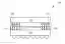
Please refer to FIG. 2 in conjunction with FIG. 3. FIG. 2 is a diagram illustrating a package on package (POP) structure 200 with pillar bump pins (e.g., copper pillar bump pins 204) according to a first embodiment of the present invention. FIG. 3 is a flowchart illustrating a method of forming a package on package (POP) structure according to a second embodiment of the present invention. Provided that substantially the same result is achieved, the steps of the flowchart shown in FIG. 3 need not be in the exact order shown and need not be contiguous; that is, other steps can be intermediate. Some steps in FIG. 3 may be omitted according to various types of embodiments or requirements. The method may be briefly summarized as follows:
Step 302: Provide a first package with a plurality of copper pillar bump pins;
Step 304: Provide a second package with a plurality of pads; and
Step 306: Form the POP structure by connecting the pillar bump pins to the pads.
The POP 200 includes a first package 202 with a plurality of pillar bump pins (e.g., copper pillar bump pins 204) and a second package 206 with a plurality of pads 208, and the first package 202 and the second package 206 further connect to each other by sticking the copper pillar bump pins 204 to the pads 208 via solder. By way of example, the first package 202 may have a memory die inside, and the second package 206 may have a logic die or another memory die inside. Table 2 indicates specifications of the POP 200 with different package sizes.
| TABLE 2 | |
| Row/Allowable pin count |
| Package size | Top package pitch | 2 | 3 | 4 | 5 | 6 |
| 12 mm*12 mm | 0.5 mm | 168 | 240 | |||
| 0.4 mm | 216 | 312 | ||||
| 0.3 mm | 288 | 420 | 544 | |||
| 0.2 mm | 440 | 648 | 848 | 1041 | ||
| 14 mm*14 mm | 0.5 mm | 200 | 288 | |||
| 0.4 mm | 240 | 372 | ||||
| 0.3 mm | 344 | 504 | 656 | 800 | ||
| 0.2 mm | 520 | 768 | 1008 | 1240 | 1464 | |
Since package pitch between rows of the copper pillar bump pins 204 is able to be shrunk to 0.2 mm pursuant to its physical and electrical characteristics, the maximum allowable pin count now extends to 1041 and 1464 for 12 mm*12 mm and 14 mm*14 mm POP structures, respectively.
It should be noted that the disclosed embodiments set forth are for illustrative purpose only, and are not meant to be limitations of the present invention. For instance, please refer to FIG. 4, which is a diagram illustrating a package on package (POP) structure 400 with pillar bump pins (e.g., copper pillar bump pins 404) according to a third embodiment of the present invention. The POP 400 includes a first package 402 with a plurality of pillar bump pins (e.g., copper pillar bump pins 404) and a second package 406 with a plurality of pads 408, and the first package 402 and the second package 406 further connect to each other by sticking the copper pillar bump pins 404 to the pads 408 via solder. By way of example, the first package 402 may have a memory die inside, and the second package 406 may have a logic die or another memory die inside. The difference between the second package 406 shown in FIG. 4 and the second package 206 shown in FIG. 2 is that the pad 408 of the second package 406 has leadframes while the pad 208 of the second package 206 does not have leadframes; in other words, the POP 400 is a leadframe package, and the POP 200 is a no-lead package. Those alternative designs concerned also belong to the scope of the present invention.
In above embodiment, the pillar part of the pillar bump pin may be preferably made of copper. However, this is for illustrative purposes only. In an alternative design, the pillar part of the pillar bump pin may be made of a different conductive material. To put it short, any POP structure using pillar bump pins to connect one package to another package for increasing the maximum allowable pin count falls within the scope of the present invention.
Those skilled in the art will readily observe that numerous modifications and alterations of the device and method may be made while retaining the teachings of the invention. Accordingly, the above disclosure should be construed as limited only by the metes and bounds of the appended claims.
Claims
What is claimed is:1. A package on package (POP) structure, comprising:
a first package, having a plurality of pillar bump pins; and
a second package, having a plurality of pads connected to the pillar bump pins, respectively.
2. The POP structure of claim 1, wherein the pillar bump pins are copper pillar bump pins.
3. The POP structure of claim 1, wherein the first package is for a memory die.
4. The POP structure of claim 1, wherein the second package is a no-lead package.
5. The POP structure of claim 1, wherein the second package is a leadframe package.
6. A method of forming a package on package (POP) structure, comprising:
providing a first package with a plurality of pillar bump pins;
providing a second package with a plurality of pads; and
forming the POP structure by connecting the pillar bump pins to the pads.
7. The method of claim 6, wherein the pillar bump pins are copper pillar bump pins.
8. The method of claim 6, wherein the first package is for a memory die.
9. The method of claim 6, wherein the second package is a no-lead package.
10. The method of claim 6, wherein the second package is a leadframe package.
Images & Drawings included:


Sources:
- United States Patent and Trademark Office - verify current appl. status at the USPTO↗
Recent applications in this class:
- » 20250293212 2025-09-18
SEMICONDUCTOR PACKAGES - » 20250293211 2025-09-18
HEAT DISSIPATION FOR STACKED INTEGRATED CIRCUIT DEVICES - » 20250293210 2025-09-18
SYSTEMS AND METHODS FOR PACKAGING A SEMICONDUCTOR DEVICE - » 20250286021 2025-09-11
SEMICONDUCTOR PACKAGE - » 20250286020 2025-09-11
SEMICONDUCTOR BONDING STRUCTURE - » 20250286019 2025-09-11
SEMICONDUCTOR PACKAGE - » 20250286018 2025-09-11
METHOD OF FABRICATING SEMICONDUCTOR BONDING STRUCTURE - » 20250286017 2025-09-11
SEMICONDUCTOR DEVICE - » 20250279399 2025-09-04
SEMICONDUCTOR DEVICES AND MANUFACTURING METHODS OF THE SAME - » 20250279398 2025-09-04
VERTICAL INTERCONNECT STRUCTURES IN THREE-DIMENSIONAL INTEGRATED CIRCUITS
Recent applications for this Assignee:
- » 20250274873 2025-08-28
METHOD AND APPARATUS OF PERFORMING POWER CONTROL ON WIRELESS COMMUNICATION DEVICE WITH POWER ESTIMATION CALIBRATION AND RELATED WIRELESS COMMUNICATION DEVICE - » 20250274501 2025-08-28
VIDEO TRANSMISSION METHOD THROUGH DYNAMIC DISPATCHING MPDUS AMONG MULTI-LINKS - » 20250266617 2025-08-21
ANTENNA INCLUDING CONDUCTIVE PLATES AND CONDUCTIVE LOOPS AND CAPABLE OF REDUCING SPURIOUS EMISSIONS - » 20250247505 2025-07-31
IMAGE PROCESSING SYSTEM AND IMAGE PROCESSING METHOD - » 20250233905 2025-07-17
Multimedia System with Dynamic Adaptation - » 20250233593 2025-07-17
Counter System and Method of Driving the Counter System with Zero Accumulated Error - » 20250227077 2025-07-10
Router-Bridge Capable of Fast Exchanging Network Packets - » 20250225301 2025-07-10
METHOD FOR PERFORMING BLOCK LEVEL EXPLORATION OF INTEGRATED CIRCUIT DESIGN, ASSOCIATED ELECTRONIC DEVICE AND ASSOCIATED COMPUTER-READABLE MEDIUM - » 20250224888 2025-07-10
APPARATUS AND METHOD FOR HANDLING SUDDEN POWER LOSS OF STORAGE DEVICE - » 20250224442 2025-07-10
Dynamic Voltage Stress Condition Optimization Method and Dynamic Voltage Stress Condition Optimization System Capable of Performing Block-based Dynamic Voltage Stress Wafer Testing Process