Semiconductor package and method of manufacturing the same
US20160020171A1
2016-01-21
14/798,833
2015-07-14
✅ Patent granted
US 9,508,565 B2
2016-11-29
-
-
Jasmine Clark
NSIP Law
2035-07-14
Abstract:
The semiconductor package according to an exemplary embodiment includes: a substrate having a plurality of circuit layers and connection pads which are provided between a plurality of insulating layers; a plated tail part of which one end is electrically connected to the connection pad; a dicing part provided in contact with the other end of the plated tail part; a molded part provided on the substrate; and molded part vias provided on the connection pads and penetrating through the molded part.
Inventors:
- Do Jae Yoo 30 🇰🇷 Suwon-Si, South Korea
- Jae Hyun LIM 30 🇰🇷 Suwon-Si, South Korea
- Eun Jung JO 19 🇰🇷 Suwon-Si, South Korea
Assignee:
- SAMSUNG ELECTRO-MECHANICS CO., LTD. 5,757 🇰🇷 Suwon-si, South Korea
- SAMSUNG ELECTRO-MECHANICS CO., LTD. 1 🇰🇪 Suwon-si, Kenya
Applicant:
Interested in similar patents?
Get notified when new applications in this technology area are published.
Classification:
H01L23/5226 » CPC main
Details of semiconductor or other solid state devices; Arrangements for conducting electric current within the device in operation from one component to another, i.e. interconnections, e.g. wires, lead frames including external interconnections consisting of a multilayer structure of conductive and insulating layers inseparably formed on the semiconductor body Via connections in a multilevel interconnection structure
H01L23/481 » CPC further
Details of semiconductor or other solid state devices; Arrangements for conducting electric current to or from the solid state body in operation, e.g. leads, terminal arrangements ; Selection of materials therefor Internal lead connections, e.g. via connections, feedthrough structures
H01L21/76802 » CPC further
Processes or apparatus adapted for the manufacture or treatment of semiconductor or solid state devices or of parts thereof; Manufacture or treatment of devices consisting of a plurality of solid state components formed in or on a common substrate or of parts thereof; Manufacture of integrated circuit devices or of parts thereof; Manufacture of specific parts of devices defined in group; Applying interconnections to be used for carrying current between separate components within a device comprising conductors and dielectrics characterised by the formation and the after-treatment of the dielectrics, e.g. smoothing by forming openings in dielectrics
H01L21/76877 » CPC further
Processes or apparatus adapted for the manufacture or treatment of semiconductor or solid state devices or of parts thereof; Manufacture or treatment of devices consisting of a plurality of solid state components formed in or on a common substrate or of parts thereof; Manufacture of integrated circuit devices or of parts thereof; Manufacture of specific parts of devices defined in group; Applying interconnections to be used for carrying current between separate components within a device comprising conductors and dielectrics characterised by the formation and the after-treatment of the conductors Filling of holes, grooves or trenches, e.g. vias, with conductive material
H01L24/11 » CPC further
Arrangements for connecting or disconnecting semiconductor or solid-state bodies; Methods or apparatus related thereto; Means for bonding being attached to, or being formed on, the surface to be connected, e.g. chip-to-package, die-attach, "first-level" interconnects; Manufacturing methods related thereto; Bump connectors ; Manufacturing methods related thereto Manufacturing methods
H01L2224/12105 » CPC further
Indexing scheme for arrangements for connecting or disconnecting semiconductor or solid-state bodies and methods related thereto as covered by; Means for bonding being attached to, or being formed on, the surface to be connected, e.g. chip-to-package, die-attach, "first-level" interconnects; Manufacturing methods related thereto; Bump connectors; Manufacturing methods related thereto; Structure, shape, material or disposition of the bump connectors prior to the connecting process Bump connectors formed on an encapsulation of the semiconductor or solid-state body, e.g. bumps on chip-scale packages
H01L2224/1302 » CPC further
Indexing scheme for arrangements for connecting or disconnecting semiconductor or solid-state bodies and methods related thereto as covered by; Means for bonding being attached to, or being formed on, the surface to be connected, e.g. chip-to-package, die-attach, "first-level" interconnects; Manufacturing methods related thereto; Bump connectors; Manufacturing methods related thereto; Structure, shape, material or disposition of the bump connectors prior to the connecting process of an individual bump connector; Core members of the bump connector Disposition
H01L23/522 IPC
Details of semiconductor or other solid state devices; Arrangements for conducting electric current within the device in operation from one component to another, i.e. interconnections, e.g. wires, lead frames including external interconnections consisting of a multilayer structure of conductive and insulating layers inseparably formed on the semiconductor body
H01L23/48 IPC
Details of semiconductor or other solid state devices Arrangements for conducting electric current to or from the solid state body in operation, e.g. leads, terminal arrangements ; Selection of materials therefor
H01L21/288 » CPC further
Processes or apparatus adapted for the manufacture or treatment of semiconductor or solid state devices or of parts thereof; Manufacture or treatment of semiconductor devices or of parts thereof the devices having at least one potential-jump barrier or surface barrier, e.g. PN junction, depletion layer or carrier concentration layer the devices having semiconductor bodies comprising elements of Group IV of the Periodic System or AB compounds with or without impurities, e.g. doping materials; Manufacture of electrodes on semiconductor bodies using processes or apparatus not provided for in groups -; Deposition of conductive or insulating materials for electrodes conducting electric current from a liquid, e.g. electrolytic deposition
H01L21/561 » CPC main
Processes or apparatus adapted for the manufacture or treatment of semiconductor or solid state devices or of parts thereof; Manufacture or treatment of semiconductor devices or of parts thereof the devices having at least one potential-jump barrier or surface barrier, e.g. PN junction, depletion layer or carrier concentration layer; Assembly of semiconductor devices using processes or apparatus not provided for in a single one of the subgroups - , e.g. sealing of a cap to a base of a container; Encapsulations, e.g. encapsulation layers, coatings Batch processing
H01L21/565 » CPC further
Processes or apparatus adapted for the manufacture or treatment of semiconductor or solid state devices or of parts thereof; Manufacture or treatment of semiconductor devices or of parts thereof the devices having at least one potential-jump barrier or surface barrier, e.g. PN junction, depletion layer or carrier concentration layer; Assembly of semiconductor devices using processes or apparatus not provided for in a single one of the subgroups - , e.g. sealing of a cap to a base of a container; Encapsulations, e.g. encapsulation layers, coatings Moulds
H01L23/3107 » CPC further
Details of semiconductor or other solid state devices; Encapsulations, e.g. encapsulating layers, coatings, e.g. for protection characterised by the arrangement or shape the device being completely enclosed
H01L22/14 » CPC further
Testing or measuring during manufacture or treatment; Reliability measurements, i.e. testing of parts without further processing to modify the parts as such; Structural arrangements therefor; Measuring as part of the manufacturing process for electrical parameters, e.g. resistance, deep-levels, CV, diffusions by electrical means
H01L21/78 » CPC further
Processes or apparatus adapted for the manufacture or treatment of semiconductor or solid state devices or of parts thereof; Manufacture or treatment of devices consisting of a plurality of solid state components formed in or on a common substrate or of parts thereof; Manufacture of integrated circuit devices or of parts thereof; Manufacture or treatment of devices consisting of a plurality of solid state components or integrated circuits formed in, or on, a common substrate with subsequent division of the substrate into plural individual devices
H01L21/768 IPC
Processes or apparatus adapted for the manufacture or treatment of semiconductor or solid state devices or of parts thereof; Manufacture or treatment of devices consisting of a plurality of solid state components formed in or on a common substrate or of parts thereof; Manufacture of integrated circuit devices or of parts thereof; Manufacture of specific parts of devices defined in group Applying interconnections to be used for carrying current between separate components within a device comprising conductors and dielectrics
H01L23/00 IPC
Details of semiconductor or other solid state devices
H01L23/31 IPC
Details of semiconductor or other solid state devices; Encapsulations, e.g. encapsulating layers, coatings, e.g. for protection characterised by the arrangement or shape
H01L23/49827 » CPC further
Details of semiconductor or other solid state devices; Arrangements for conducting electric current to or from the solid state body in operation, e.g. leads, terminal arrangements ; Selection of materials therefor consisting of soldered constructions; Leads, on insulating substrates, Via connections through the substrates, e.g. pins going through the substrate, coaxial cables
H01L21/4853 » CPC further
Processes or apparatus adapted for the manufacture or treatment of semiconductor or solid state devices or of parts thereof; Manufacture or treatment of semiconductor devices or of parts thereof the devices having at least one potential-jump barrier or surface barrier, e.g. PN junction, depletion layer or carrier concentration layer; Manufacture or treatment of parts, e.g. containers, prior to assembly of the devices, using processes not provided for in a single one of the subgroups -; Conductive parts; Leads on or in insulating or insulated substrates, e.g. metallisation Connection or disconnection of other leads to or from a metallisation, e.g. pins, wires, bumps
H01L22/32 » CPC further
Testing or measuring during manufacture or treatment; Reliability measurements, i.e. testing of parts without further processing to modify the parts as such; Structural arrangements therefor; Structural arrangements specially adapted for testing or measuring during manufacture or treatment, or specially adapted for reliability measurements Additional lead-in metallisation on a device or substrate, e.g. additional pads or pad portions, lines in the scribe line, sacrificed conductors
H01L23/145 » CPC further
Details of semiconductor or other solid state devices; Mountings, e.g. non-detachable insulating substrates characterised by the material or its electrical properties Organic substrates, e.g. plastic
H01L23/49811 » CPC further
Details of semiconductor or other solid state devices; Arrangements for conducting electric current to or from the solid state body in operation, e.g. leads, terminal arrangements ; Selection of materials therefor consisting of soldered constructions; Leads, on insulating substrates, Additional leads joined to the metallisation on the insulating substrate, e.g. pins, bumps, wires, flat leads
H01L2924/0002 » CPC further
Indexing scheme for arrangements or methods for connecting or disconnecting semiconductor or solid-state bodies as covered by; Technical content checked by a classifier Not covered by any one of groups , and
H01L23/14 IPC
Details of semiconductor or other solid state devices; Mountings, e.g. non-detachable insulating substrates characterised by the material or its electrical properties
H01L23/498 IPC
Details of semiconductor or other solid state devices; Arrangements for conducting electric current to or from the solid state body in operation, e.g. leads, terminal arrangements ; Selection of materials therefor consisting of soldered constructions Leads, on insulating substrates,
H05K1/00 » CPC further
Printed circuits
H05K1/00 » CPC further
Printed circuits
H01L21/56 IPC
Processes or apparatus adapted for the manufacture or treatment of semiconductor or solid state devices or of parts thereof; Manufacture or treatment of semiconductor devices or of parts thereof the devices having at least one potential-jump barrier or surface barrier, e.g. PN junction, depletion layer or carrier concentration layer; Assembly of semiconductor devices using processes or apparatus not provided for in a single one of the subgroups - , e.g. sealing of a cap to a base of a container Encapsulations, e.g. encapsulation layers, coatings
H01L21/48 IPC
Processes or apparatus adapted for the manufacture or treatment of semiconductor or solid state devices or of parts thereof; Manufacture or treatment of semiconductor devices or of parts thereof the devices having at least one potential-jump barrier or surface barrier, e.g. PN junction, depletion layer or carrier concentration layer Manufacture or treatment of parts, e.g. containers, prior to assembly of the devices, using processes not provided for in a single one of the subgroups -
Description
CROSS-REFERENCE TO RELATED APPLICATION
This application claims the priority and benefit of Korean Patent Application No. 10-2014-0090994 filed on Jul. 18, 2014, with the Korean Intellectual Property Office, the disclosure of which is incorporated herein by reference.
BACKGROUND
The present disclosure relates to a semiconductor package and a method of manufacturing the same.
In accordance with the trend for the miniaturization of and high performance in information technology (IT) devices, mass storage memories and high performance integrated circuits (IC) have been required for use therein. Existing two-dimensional (2D) packages have reached the technical limits of simultaneously achieving the levels of integration and high performance that are currently required. In order to overcome these technical limits, a large amount of research aimed at manufacturing three-dimensional (3D) packages using a variety of methods has been conducted, and the development of new types of interconnection technology is required. As one of these methods, a double side packaging method in which both sides of a printed circuit board (PCB) are used has been used for packages provided in mobile devices.
SUMMARY
An aspect of the present disclosure provides a semiconductor package enabling an open/short test on a substrate by implementing a plated tail which is electrically connected to a plating line by forming solder balls in a sawing region of the package, and a method of manufacturing the same.
An aspect of the present disclosure also provides a semiconductor package enabling an open/short test on a substrate by implementing a plated tail which is electrically connected to a plating line by an electroless plating process, after additionally forming a molded part via hole in a sawing region of the package, and a method of manufacturing the same.
An aspect of the present disclosure also provides a semiconductor package capable of preventing defect such as delamination of a pad by leaving a plated tail after performing a sawing process, and a method of manufacturing the same.
According to an aspect of the present disclosure, a semiconductor package may include: a substrate having a plurality of circuit layers and connection pads formed between a plurality of insulating layers; a plated tail part of which one end is electrically connected to the connection pad; a dicing part formed so as to be in contact with the other end of the plated tail part; a molded part formed on the substrate; and molded part vias formed on the connection pads and formed so as to penetrate through the molded part.
The semiconductor package may further include a plurality of vias that electrically connect the plurality of circuit layers to each other.
According to another aspect of the present disclosure, a method of manufacturing a semiconductor package may include: preparing a substrate having a plurality of circuit layers and connection pads formed between a plurality of insulating layers and having openings for testing; forming a molded part on the substrate; forming molded part via holes so as to expose upper portions of the connection pads and penetrate through the molded part; and forming molded part vias by plating the molded part via holes.
In the preparing of the substrate, a plated tail part of which one end is electrically connected to the connection pad; and a dicing part formed so as to be in contact with the other end of the plated tail part or include a portion of the other end of the plated tail part may be formed.
In the preparing of the substrate, a plurality of vias that electrically connect the plurality of circuit layers to each other may be formed.
The dicing part may include the openings for testing.
The method may further include, after the preparing of the substrate, performing an open-short test.
The method may further include, before the forming of the molded part, forming solder balls in the openings for testing.
The method may further include, after the forming of the molding via holes, forming a seed layer by performing an electroless plating process for the molded part via holes and the openings for testing.
The method may further include, after the forming of the molded part vias, dicing and separating the dicing part.
Features and advantages of the present disclosure will be more obvious from the following description with reference to the accompanying drawings.
The terms and words used in the present specification and claims should not be interpreted as being limited to typical meanings or dictionary definitions, but should be interpreted as having meanings and concepts relevant to the technical scope of the present disclosure based on the rule according to which an inventor can appropriately define the concept of the term to describe most appropriately the best method he or she knows for carrying out the disclosure.
BRIEF DESCRIPTION OF DRAWINGS
The above and other aspects, features and advantages of the present disclosure will be more clearly understood from the following detailed description taken in conjunction with the accompanying drawings, in which:
FIG. 1 is a cross-sectional view of a structure of a semiconductor package according to an exemplary embodiment in the present disclosure;
FIG. 2 is a plan view of the semiconductor package according to an exemplary embodiment in the present disclosure;
FIGS. 3 through 8 are views illustrating a method of manufacturing a semiconductor package according to a first exemplary embodiment in the present disclosure; and
FIGS. 9 through 13 are views illustrating a method of manufacturing a semiconductor package according to a second exemplary embodiment in the present disclosure.
DETAILED DESCRIPTION
Exemplary embodiments of the present disclosure will now be described in detail with reference to the accompanying drawings.
The disclosure may, however, be embodied in many different forms and should not be construed as being limited to the embodiments set forth herein. Rather, these embodiments are provided so that this disclosure will be thorough and complete, and will fully convey the scope of the disclosure to those skilled in the art.
In the drawings, the shapes and dimensions of elements maybe exaggerated for clarity, and the same reference numerals will be used throughout to designate the same or like elements.
Semiconductor Package
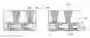
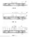
FIG. 1 is a cross-sectional view of a semiconductor package according to an exemplary embodiment in the present disclosure.
As shown in FIG. 1, the semiconductor package may include a substrate 100 having a plurality of circuit layers 101 and connection pads 104 formed between a plurality of insulating layers 103, a plated tail part B of which one end is electrically connected to the connection pad 104, a dicing part A formed so as to be in contact with the other end of the plated tail part B, a molded part 300 formed on the substrate 100, and molded part vias 302 formed on the connection pads 104 and formed so as to penetrate through the molded part 300.
In addition, the semiconductor package may be provided with a plurality of vias 102 that electrically connect the plurality of circuit layers 101 to each other.
Here, as the insulating layer 102, a resin insulating layer may be used. As a material of the resin insulating layer, a thermosetting resin such as an epoxy resin, a thermoplastic resin such as polyimide, or a resin having a reinforcement material such as glass fiber or inorganic filler impregnated in the thermosetting resin and the thermoplastic resin, for example, prepreg may be used. In addition, a thermosetting resin, a photo-curable resin, and/or the like may be used. However, the material of the resin insulating layer is not particularly limited thereto.
In addition, the circuit layers 101 may be made of any material without being limited as long as it is used as a conductive metal for a circuit and be typically made of copper in a printed circuit board.
A surface treatment layer (not shown) may be further formed on the connection pad 104, if necessary. In this case, the surface treatment layer is not particularly limited as long as it is known in the art, but be formed by, for example, an electro gold plating, an immersion gold plating, an organic solderability preservative (OSP) or an immersion tin plating, an immersion silver plating, an electroless nickel and immersion gold (ENIG), a direct immersion gold (DIG) plating, a hot air solder leveling (HASL), or the like.
Here, due to a presence of the plated tail part B, mechanical reliability may be increased. For example, due to the plated tail part B formed so as to be connected to one end of the connection pad 104, defect such as delamination of the connection pad 104 may be reduced.
In addition, in case of a surface mounting, since solder resist simultaneously covers the connection pad 104 and the plated tail part B formed so as to be connected to the connection pad 104, a cover region may be increased, thereby reducing a delamination phenomenon of the connection pad.
In addition, the molded part 300 may be formed on the substrate 100.
In this case, the molded part 300 may be made of a material of silicone gel, epoxy molded compound (EMC), or the like, but is not particularly limited thereto.
FIG. 2 is a plan view of the semiconductor package according to an exemplary embodiment in the present disclosure.
The plated tail part B that is electrically connected to one end of the connection pad 104 may be formed.
Method of Manufacturing Semiconductor Package
First Exemplary Embodiment
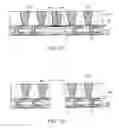
FIGS. 3 through 8 are views illustrating a method of manufacturing a semiconductor package according to a first exemplary embodiment in the present disclosure.
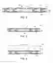
As shown in FIG. 3, a substrate 100 having a plurality of circuit layers 101 and connection pads 104 formed between a plurality of insulating layers 103 and having openings 105 for testing is prepared.
Here, a plurality of vias 102 that electrically connect the plurality of circuit layers 101 to each other may be further formed.
Here, as the insulating layer 102, a resin insulating layer may be used. As a material of the resin insulating layer, a thermosetting resin such as an epoxy resin, a thermoplastic resin such as polyimide, or a resin having a reinforcement material such as glass fiber or inorganic filler impregnated in the thermosetting resin and the thermoplastic resin, for example, prepreg may be used. In addition, a thermosetting resin, a photo-curable resin, and/or the like may be used. However, the material of the resin insulating layer is not particularly limited thereto.
In addition, the circuit layers 101 may be made of any material without being limited as long as it is used as a conductive metal for a circuit and be typically made of copper in a printed circuit board.
A surface treatment layer (not shown) may be further formed on the connection pad 104, if necessary. In this case, the surface treatment layer is not particularly limited as long as it is known in the art, but be formed by, for example, an electro gold plating, an immersion gold plating, an organic solderability preservative (OSP) or an immersion tin plating, an immersion silver plating, an electroless nickel and immersion gold (ENIG), a direct immersion gold (DIG) plating, a hot air solder leveling (HASL), or the like.
In addition, a plated tail part B of which one end is electrically connected to the connection pad 104 and a dicing part A formed so as to be in contact with the other end of the plated tail part B and include a portion of the other end of the plated tail part B may be formed.
In this case, the opening 105 for testing may be formed so as to be included in the dicing part A and may be formed so as to expose the insulating layer 103.
In addition, the opening 105 may have various sizes and may be formed at any position in the dicing part A.
Next, an open-short test may be performed at a substrate level in which the opening 105 is formed.
Specifically, the plated tail part B connected to one end of the connection pad 104 may be discontinuously formed in the dicing part A, due to the opening 105 formed on the substrate 100.
Thereby, a conduction line of the plated tail part B is blocked, such that the open-short test may be performed at the substrate level.
As shown in FIG. 4, the opening 105 may be filled with solder by performing a soldering process.
Thereby, a conduction line of the dicing part A may be connected. This allows electricity to flow in a plated region in order to perform an electroplating.
As shown in FIG. 5, a molded part 300 may be formed so as to cover an upper portion of the substrate 100.
In this case, the molded part 300 may be made of a material of silicone gel, epoxy molded compound (EMC), or the like, but is not particularly limited thereto.
As shown in FIG. 6, molded part via holes 301 may be formed. In this case, the molded part via hole 301 may be formed so as to expose an upper portion of the connection pad 104 and penetrate through the molded part 300.
Here, the molded part via hole 301 may be machined by using a laser drill such as a CO2 laser drill, a YAG laser drill, or the like, but is not particularly thereto.
As shown in FIG. 7, molded part vias 302 may be formed by plating the molded part via holes 301.
As shown in FIG. 8, the dicing part A may be diced. In this case, a portion of the plated tail part B may be left.
Here, due to a presence of the plated tail part B, mechanical reliability may be increased. For example, due to the plated tail part B formed so as to be connected to one end of the connection pad 104, defect such as delamination of the connection pad 104 may be reduced.
In addition, in case of a surface mounting, since solder resist simultaneously covers the connection pad 104 and the plated tail part B formed so as to be connected to the connection pad 104, a cover region may be increased, thereby reducing a delamination phenomenon of the connection pad.
Second Exemplary Embodiment
FIGS. 9 through 13 are views illustrating a method of manufacturing a semiconductor package according to a second exemplary embodiment in the present disclosure.
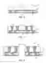
As shown in FIG. 9, a substrate 100 having a plurality of circuit layers 101 and connection pads 104 formed between a plurality of insulating layers 103 and having openings 105 for testing is prepared.
Here, a plurality of vias 102 that electrically connect the plurality of circuit layers 101 to each other may be further formed.
In addition, as the insulating layer 102, a resin insulating layer may be used. As a material of the resin insulating layer, a thermosetting resin such as an epoxy resin, a thermoplastic resin such as polyimide, or a resin having a reinforcement material such as glass fiber or inorganic filler impregnated in the thermosetting resin and the thermoplastic resin, for example, prepreg may be used. In addition, a thermosetting resin, a photo-curable resin, and/or the like may be used. However, the material of the resin insulating layer is not particularly limited thereto.
In addition, the circuit layers 101 may be made of any material without being limited as long as it is used as a conductive metal for a circuit and be typically made of copper in a printed circuit board.
A surface treatment layer (not shown) may be further formed on the connection pad 104, if necessary. In this case, the surface treatment layer is not particularly limited as long as it is known in the art, but be formed by, for example, an electro gold plating, an immersion gold plating, an organic solderability preservative (OSP) or an immersion tin plating, an immersion silver plating, an electroless nickel and immersion gold (ENIG), a direct immersion gold (DIG) plating, a hot air solder leveling (HASL), or the like.
In addition, a plated tail part B of which one end is electrically connected to the connection pad 104 and a dicing part A formed so as to be in contact with the other end of the plated tail part B and include a portion of the other side of the plated tail part B may be formed.
In this case, the opening 105 for testing may be formed so as to be included in the dicing part A and may be formed so as to expose the insulating layer 103.
In addition, the opening 105 may have various sizes and may be formed at any position in the dicing part A.
Next, an open-short test may be performed on a substrate level in which the opening 105 is formed.
Specifically, the plated tail part B connected to one end of the connection pad 104 may be discontinuously formed in the dicing part A, due to the opening 105 formed on the substrate 100.
Thereby, a conduction line of the plated tail part B is blocked, such that the open-short test may be performed at the substrate level.
As shown in FIG. 10, a molded part 300 may be formed so as to cover an upper portion of the substrate 100.
In this case, the molded part 300 may be made of a material of silicone gel, epoxy molded compound (EMC), or the like, but is not particularly limited thereto.
As shown in FIG. 11, molded part via holes 301 may be formed so as to penetrate through the molded part 300.
In this case, the molded part via hole 301 may be formed so as to expose an upper portion of the connection pad 104 and penetrate through the molded part 300.
As shown in FIG. 12, an electroless plated layer 303 may be formed.
In this case, the electroless plated layer 303 may fill the opening 105 of the dicing part A.
Thereby, a conduction line of the dicing part A may be connected. This allows electricity to flow in a plated region in order to perform an electroplating.
Since the electroless plating process is a plating process for an insulator, reaction by electrically charged ions may not be expected. The electroless plating process may be performed by a precipitation reaction, and the precipitation reaction may be promoted by catalyst. In order to precipitate copper from a plating solution, the catalyst needs to be attached to a surface of a material to be plated. This means that the electroless plating requires a plurality of pre-processes.
As an example, the electroless plating process may include a cleanet operation, a soft etching operation, a pre-catalyst operation, a catalyst treatment operation, an accelerator operation, an electroless plating operation, and an anti-oxidation treatment operation.
In the cleanet operation, after oxides or foreign materials, particularly, oil, or the like that are present on upper and lower copper foil surfaces are removed with chemicals containing an acid or alkali surface active agent, the surface active agent may be perfectly cleaned. In the soft etching operation, fine roughness (e.g., about 1 μm to 2 μm) is formed on the upper and lower copper foil surfaces, such that copper particles may be closely adhered to each other in the plating process and contaminants that are not processed in the cleanet operation may be removed. In the pre-catalyst operation, the substrate is immersed in catalyst chemicals having low concentration, thereby preventing the chemicals used in a catalyst treatment operation from being contaminated or a concentration thereof from being changed. Moreover, since the substrate is immersed in advance in a bath having the chemicals made of the same component, the catalyst treatment may be further activated. The pre-catalyst operation may use catalyst chemicals which are diluted at 1% and 3%.
In the catalyst treatment operation, catalyst particles may be coated on copper foil of the substrate and surfaces of the insulating resin layer (i.e., side walls of the via hole). As the catalyst particle, a Pd—Sn compound may be used and the Pd—Sn compound may serve to promote the plating by a coupling of Cu2+ and Pd2− which are particles to be plated. In the electroless plating operation, the plating solution may be made of CuSO4, HCHO, NaOH, and other stabilizers. In order to consistently perform a plating reaction, a chemical reaction needs to be balanced. To this end, it is important to control composition of the plating solution. In order to maintain the composition, a proper supply of insufficient components, mechanical stirring, a circulation system of the plating solution, and the like need to be properly operated. A filter for products generated as a result of the reaction may be required and a use time of the plating solution may be extended by utilizing the filter.
In the anti-oxidation treatment operation, an anti-oxidation layer may be coated on the overall surface in order to prevent the plated layer from being oxidized due to the alkali component which is left after performing the electroless plating process.
However, since the above-mentioned electroless plating process generally has deteriorated physical characteristics as compared to the electroplating process, the electroless plated layer may be formed to be thin.
Next, after the electroless plated layer 303 is formed, molded part vias 302 may be formed by performing the electroplating process for the molded part via holes 301.
As shown in FIG. 13, the dicing part A may be diced. In this case, a portion of the plated tail part B may be left.
Here, due to a presence of the plated tail part B, mechanical reliability may be increased. For example, due to the plated tail part B formed so as to be connected to one end of the connection pad 104, defects such as delamination of the connection pad 104 may be reduced.
In addition, in the case of a surface mounting, since solder resist simultaneously covers the connection pad 104 and the plated tail part B formed so as to be connected to the connection pad 104, a cover region may be increased, thereby reducing a delamination phenomenon of the connection pad.
While exemplary embodiments have been shown and described above, it will be apparent to those skilled in the art that modifications and variations could be made without departing from the scope of the present invention as defined by the appended claims.
Claims
What is claimed is:1. A semiconductor package comprising:
a substrate having a plurality of circuit layers and connection pads which are provided between a plurality of insulating layers;
a plated tail part of which one end is electrically connected to the connection pad;
a dicing part provided in contact with the other end of the plated tail part;
a molded part provided on the substrate; and
molded part vias provided on the connection pads and penetrating through the molded part.
2. The semiconductor package of claim 1, further comprising a plurality of vias that electrically connect the plurality of circuit layers to each other.
3. A method of manufacturing a semiconductor package, the method comprising:
preparing a substrate having openings for testing and including a plurality of circuit layers and connection pads which are provided between a plurality of insulating layers;
forming a molded part on the substrate;
forming molded part via holes which expose upper portions of the connection pads and penetrate through the molded part; and
forming molded part vias by performing plating on the molded part via holes.
4. The method of claim 3, wherein the substrate is prepared to include: a plated tail part of which one end is electrically connected to the connection pad; and a dicing part formed to be in contact with the other end of the plated tail part or to include a portion of the other end of the plated tail part.
5. The method of claim 3, wherein the substrate is prepared to include a plurality of vias that electrically connect the plurality circuit layers to each other.
6. The method of claim 4, wherein the dicing part includes the openings for testing.
7. The method of claim 3, further comprising, after the preparing of the substrate, performing an open-short test.
8. The method of claim 3, further comprising, before the forming of the molded part, forming solder balls in the openings for testing.
9. The method of claim 3, further comprising, after the forming of the molded via holes, forming a seed layer by performing electroless plating on the molded part via holes and the openings for testing.
10. The method of claim 4, further comprising, after the forming of the molded part vias, dicing the substrate in the dicing part to be separated into packages.
Images & Drawings included:
Sources:
- United States Patent and Trademark Office - verify current appl. status at the USPTO↗
Similar patent applications:
- » 20130309818
Manufacturing method of substrate for a semiconductor package, manufacturing method of semiconductor package, substrate for a semiconductor package and semiconductor package - » 20100213620
Manufacturing method of substrate for a semiconductor package, manufacturing method of semiconductor package, substrate for a semiconductor package and semiconductor package - » 20120064666
MANUFACTURING METHOD OF SUBSTRATE FOR A SEMICONDUCTOR PACKAGE, MANUFACTURING METHOD OF SEMICONDUCTOR PACKAGE, SUBSTRATE FOR A SEMICONDUCTOR PACKAGE AND SEMICONDUCTOR PACKAGE - » 20250149527
SEMICONDUCTOR PACKAGE, SEMICONDUCTOR PACKAGE INTERMEDIATE, REDISTRIBUTION LAYER CHIP, REDISTRIBUTION LAYER CHIP INTERMEDIATE, METHOD OF MANUFACTURING SEMICONDUCTOR PACKAGE, AND METHOD OF MANUFACTURING SEMICONDUCTOR PACKAGE INTERMEDIATE - » 20240096808
SEMICONDUCTOR PACKAGE, MANUFACTURING METHOD OF SEMICONDUCTOR PACKAGE, AND INTERPOSER GROUP - » 20240145326
SEMICONDUCTOR PACKAGE MANUFACTURING METHOD AND SEMICONDUCTOR PACKAGE - » 20120153457
Semiconductor package manufacturing method and semiconductor package - » 20140035157
SEMICONDUCTOR PACKAGE, MANUFACTURING METHOD THEREOF, AND SEMICONDUCTOR PACKAGE MANUFACTURING MOLD - » 20100133349
Semiconductor package, method of manufacturing semiconductor package, electronic component, and method of manufacturing electronic component - » 10736568
Semiconductor device package manufacturing method and semiconductor device package manufactured by the method
Recent applications in this class:
- » 20250293150 2025-09-18
INTEGRATED CIRCUITS DEVICES, SYSTEMS AND METHODS - » 20250293149 2025-09-18
IC DIE FABRICATION WITH SELF-ALIGNMENT OF MULTI-LEVEL FEATURES - » 20250285962 2025-09-11
SEMICONDUCTOR DEVICE AND METHOD FOR MANUFACTURING THE SAME - » 20250285961 2025-09-11
SEMICONDUCTOR DEVICE AND METHOD OF MANUFACTURING SEMICONDUCTOR DEVICE - » 20250285960 2025-09-11
SEMICONDUCTOR DEVICES HAVING A PATTERNED CONTACT - » 20250279353 2025-09-04
MIDDLE-OF-LINE INTERCONNECT STRUCTURE AND MANUFACTURING METHOD - » 20250279352 2025-09-04
INTERCONNECT STRUCTURE - » 20250279351 2025-09-04
SEMICONDUCTOR STRUCTURE - » 20250273566 2025-08-28
SEMICONDUCTOR DEVICE AND METHOD OF MANUFACTURING THE SAME - » 20250273565 2025-08-28
PACKAGE STRUCTURE AND METHOD OF FORMING THE SAME
Recent applications for this Assignee:
- » 20250291200 2025-09-18
CAMERA MODULE - » 20250291156 2025-09-18
OPTICAL IMAGING SYSTEM - » 20250291155 2025-09-18
OPTICAL IMAGING SYSTEM - » 20250287502 2025-09-11
CIRCUIT BOARD AND MANUFACTURING METHOD THEREOF - » 20250287498 2025-09-11
PRINTED CIRCUIT BOARD - » 20250285957 2025-09-11
INTERPOSER SUBSTRATE AND SEMICONDUCTOR PACKAGE INCLUDING THE SAME - » 20250285940 2025-09-11
PRINTED CIRCUIT BOARD - » 20250284099 2025-09-11
OPTICAL IMAGING SYSTEM - » 20250284098 2025-09-11
LENS MODULE - » 20250284094 2025-09-11
OPTICAL IMAGING SYSTEM