Semiconductor die arrangement
US20160133547A1
2016-05-12
14/865,985
2015-09-25
✅ Patent granted
US 9,685,396 B2
2017-06-20
-
-
Teresa M Arroyo
Rajeev Madnawat
2035-09-25
Abstract:
A semiconductor die arrangement comprising a first die including at least one semiconductor device; a second die including at least one semiconductor device; a lead frame associated with the first die and comprising one or more lead fingers, wherein the second die is mounted on one of the lead fingers and electrically connected to a further element by a bond wire.
Assignee:
- NXP B.V. 5,639 🇳🇱 Eindhoven, Netherlands
Applicant:
Interested in similar patents?
Get notified when new applications in this technology area are published.
Classification:
H01L23/4951 » CPC main
Details of semiconductor or other solid state devices; Arrangements for conducting electric current to or from the solid state body in operation, e.g. leads, terminal arrangements ; Selection of materials therefor consisting of soldered constructions; Lead-frames or other flat leads characterised by the die pad Chip-on-leads or leads-on-chip techniques, i.e. inner lead fingers being used as die pad
H01L21/4825 » CPC further
Processes or apparatus adapted for the manufacture or treatment of semiconductor or solid state devices or of parts thereof; Manufacture or treatment of semiconductor devices or of parts thereof the devices having at least one potential-jump barrier or surface barrier, e.g. PN junction, depletion layer or carrier concentration layer; Manufacture or treatment of parts, e.g. containers, prior to assembly of the devices, using processes not provided for in a single one of the subgroups -; Conductive parts; Flat leads, e.g. lead frames with or without insulating supports Connection or disconnection of other leads to or from flat leads, e.g. wires, bumps, other flat leads
H01L21/565 » CPC further
Processes or apparatus adapted for the manufacture or treatment of semiconductor or solid state devices or of parts thereof; Manufacture or treatment of semiconductor devices or of parts thereof the devices having at least one potential-jump barrier or surface barrier, e.g. PN junction, depletion layer or carrier concentration layer; Assembly of semiconductor devices using processes or apparatus not provided for in a single one of the subgroups - , e.g. sealing of a cap to a base of a container; Encapsulations, e.g. encapsulation layers, coatings Moulds
H01L23/3114 » CPC further
Details of semiconductor or other solid state devices; Encapsulations, e.g. encapsulating layers, coatings, e.g. for protection characterised by the arrangement or shape the device being completely enclosed the device being a chip scale package, e.g. CSP
H01L23/4952 » CPC further
Details of semiconductor or other solid state devices; Arrangements for conducting electric current to or from the solid state body in operation, e.g. leads, terminal arrangements ; Selection of materials therefor consisting of soldered constructions; Lead-frames or other flat leads; Additional leads the additional leads being a bump or a wire
H01L23/49513 » CPC further
Details of semiconductor or other solid state devices; Arrangements for conducting electric current to or from the solid state body in operation, e.g. leads, terminal arrangements ; Selection of materials therefor consisting of soldered constructions; Lead-frames or other flat leads characterised by the die pad having bonding material between chip and die pad
H01L23/49562 » CPC further
Details of semiconductor or other solid state devices; Arrangements for conducting electric current to or from the solid state body in operation, e.g. leads, terminal arrangements ; Selection of materials therefor consisting of soldered constructions; Lead-frames or other flat leads; Geometry of the lead-frame for devices being provided for in
H01L23/49575 » CPC further
Details of semiconductor or other solid state devices; Arrangements for conducting electric current to or from the solid state body in operation, e.g. leads, terminal arrangements ; Selection of materials therefor consisting of soldered constructions; Lead-frames or other flat leads Assemblies of semiconductor devices on lead frames
H01L25/0657 » CPC further
Assemblies consisting of a plurality of individual semiconductor or other solid state devices ; Multistep manufacturing processes thereof all the devices being of a type provided for in the same subgroup of groups - , e.g. assemblies of rectifier diodes the devices not having separate containers the devices being of a type provided for in group Stacked arrangements of devices
H01L23/495 IPC
Details of semiconductor or other solid state devices; Arrangements for conducting electric current to or from the solid state body in operation, e.g. leads, terminal arrangements ; Selection of materials therefor consisting of soldered constructions Lead-frames or other flat leads
H01L21/48 IPC
Processes or apparatus adapted for the manufacture or treatment of semiconductor or solid state devices or of parts thereof; Manufacture or treatment of semiconductor devices or of parts thereof the devices having at least one potential-jump barrier or surface barrier, e.g. PN junction, depletion layer or carrier concentration layer Manufacture or treatment of parts, e.g. containers, prior to assembly of the devices, using processes not provided for in a single one of the subgroups -
H01L21/56 IPC
Processes or apparatus adapted for the manufacture or treatment of semiconductor or solid state devices or of parts thereof; Manufacture or treatment of semiconductor devices or of parts thereof the devices having at least one potential-jump barrier or surface barrier, e.g. PN junction, depletion layer or carrier concentration layer; Assembly of semiconductor devices using processes or apparatus not provided for in a single one of the subgroups - , e.g. sealing of a cap to a base of a container Encapsulations, e.g. encapsulation layers, coatings
H01L23/31 IPC
Details of semiconductor or other solid state devices; Encapsulations, e.g. encapsulating layers, coatings, e.g. for protection characterised by the arrangement or shape
H01L25/065 IPC
Assemblies consisting of a plurality of individual semiconductor or other solid state devices ; Multistep manufacturing processes thereof all the devices being of a type provided for in the same subgroup of groups - , e.g. assemblies of rectifier diodes the devices not having separate containers the devices being of a type provided for in group
H01L24/48 » CPC further
Arrangements for connecting or disconnecting semiconductor or solid-state bodies; Methods or apparatus related thereto; Means for bonding being attached to, or being formed on, the surface to be connected, e.g. chip-to-package, die-attach, "first-level" interconnects; Manufacturing methods related thereto; Wire connectors; Manufacturing methods related thereto; Structure, shape, material or disposition of the wire connectors after the connecting process of an individual wire connector
H01L24/06 » CPC further
Arrangements for connecting or disconnecting semiconductor or solid-state bodies; Methods or apparatus related thereto; Means for bonding being attached to, or being formed on, the surface to be connected, e.g. chip-to-package, die-attach, "first-level" interconnects; Manufacturing methods related thereto; Bonding areas ; Manufacturing methods related thereto; Structure, shape, material or disposition of the bonding areas prior to the connecting process of a plurality of bonding areas
H01L24/29 » CPC further
Arrangements for connecting or disconnecting semiconductor or solid-state bodies; Methods or apparatus related thereto; Means for bonding being attached to, or being formed on, the surface to be connected, e.g. chip-to-package, die-attach, "first-level" interconnects; Manufacturing methods related thereto; Layer connectors, e.g. plate connectors, solder or adhesive layers; Manufacturing methods related thereto; Structure, shape, material or disposition of the layer connectors prior to the connecting process of an individual layer connector
H01L24/32 » CPC further
Arrangements for connecting or disconnecting semiconductor or solid-state bodies; Methods or apparatus related thereto; Means for bonding being attached to, or being formed on, the surface to be connected, e.g. chip-to-package, die-attach, "first-level" interconnects; Manufacturing methods related thereto; Layer connectors, e.g. plate connectors, solder or adhesive layers; Manufacturing methods related thereto; Structure, shape, material or disposition of the layer connectors after the connecting process of an individual layer connector
H01L24/73 » CPC further
Arrangements for connecting or disconnecting semiconductor or solid-state bodies; Methods or apparatus related thereto Means for bonding being of different types provided for in two or more of groups , , , , , , ,
H01L2224/0603 » CPC further
Indexing scheme for arrangements for connecting or disconnecting semiconductor or solid-state bodies and methods related thereto as covered by; Means for bonding being attached to, or being formed on, the surface to be connected, e.g. chip-to-package, die-attach, "first-level" interconnects; Manufacturing methods related thereto; Bonding areas; Manufacturing methods related thereto; Structure, shape, material or disposition of the bonding areas prior to the connecting process of a plurality of bonding areas; Structure Bonding areas having different sizes, e.g. different heights or widths
H01L2224/73265 » CPC further
Indexing scheme for arrangements for connecting or disconnecting semiconductor or solid-state bodies and methods related thereto as covered by; Means for bonding being of different types provided for in two or more of groups; Location after the connecting process on different surfaces Layer and wire connectors
H01L2224/92247 » CPC further
Indexing scheme for arrangements for connecting or disconnecting semiconductor or solid-state bodies and methods related thereto as covered by; Methods for connecting semiconductor or solid state bodies including different methods provided for in two or more of groups - ; Specific sequence of method steps; Connecting different surfaces of the semiconductor or solid-state body with connectors of different types; Sequential connecting processes the first connecting process involving a layer connector the second connecting process involving a wire connector
H01L2924/00014 » CPC further
Indexing scheme for arrangements or methods for connecting or disconnecting semiconductor or solid-state bodies as covered by; Technical content checked by a classifier the subject-matter covered by the group, the symbol of which is combined with the symbol of this group, being disclosed without further technical details
H01L2924/1203 » CPC further
Indexing scheme for arrangements or methods for connecting or disconnecting semiconductor or solid-state bodies as covered by; Details of semiconductor or other solid state devices to be connected; Device type; Passive devices, e.g. 2 terminal devices Rectifying Diode
H01L2924/13033 » CPC further
Indexing scheme for arrangements or methods for connecting or disconnecting semiconductor or solid-state bodies as covered by; Details of semiconductor or other solid state devices to be connected; Device type; Discrete devices, e.g. 3 terminal devices; Thyristor TRIAC - Triode for Alternating Current - A bidirectional switching device containing two thyristor structures with common gate contact
H01L2924/13034 » CPC further
Indexing scheme for arrangements or methods for connecting or disconnecting semiconductor or solid-state bodies as covered by; Details of semiconductor or other solid state devices to be connected; Device type; Discrete devices, e.g. 3 terminal devices; Thyristor Silicon Controlled Rectifier [SCR]
H01L23/48 IPC
Details of semiconductor or other solid state devices Arrangements for conducting electric current to or from the solid state body in operation, e.g. leads, terminal arrangements ; Selection of materials therefor
H01L29/40 IPC
Semiconductor devices adapted for rectifying, amplifying, oscillating or switching, or capacitors or resistors with at least one potential-jump barrier or surface barrier, e.g. PN junction depletion layer or carrier concentration layer; Details of semiconductor bodies or of electrodes thereof; Multistep manufacturing processes therefor Electrodes ; Multistep manufacturing processes therefor
H01L23/34 IPC
Details of semiconductor or other solid state devices Arrangements for cooling, heating, ventilating or temperature compensation ; Temperature sensing arrangements
H01L21/00 IPC
Processes or apparatus adapted for the manufacture or treatment of semiconductor or solid state devices or of parts thereof
H01L23/00 IPC
Details of semiconductor or other solid state devices
H01L24/49 » CPC further
Arrangements for connecting or disconnecting semiconductor or solid-state bodies; Methods or apparatus related thereto; Means for bonding being attached to, or being formed on, the surface to be connected, e.g. chip-to-package, die-attach, "first-level" interconnects; Manufacturing methods related thereto; Wire connectors; Manufacturing methods related thereto; Structure, shape, material or disposition of the wire connectors after the connecting process of a plurality of wire connectors
H01L2924/1301 » CPC further
Indexing scheme for arrangements or methods for connecting or disconnecting semiconductor or solid-state bodies as covered by; Details of semiconductor or other solid state devices to be connected; Device type; Discrete devices, e.g. 3 terminal devices Thyristor
H01L23/52 IPC
Details of semiconductor or other solid state devices Arrangements for conducting electric current within the device in operation from one component to another, i.e. interconnections, e.g. wires, lead frames
Description
This disclosure relates to semiconductor die arrangement. In particular, it relates to a semiconductor die arrangement comprising at least two or at least three distinct dies.
An integrated circuit package may include a plurality of dies. Each of the dies may have a semiconductor device(s) formed therein. The dies are typically arranged in a stacked configuration and thus comprise a base die and one or more further dies stacked on top of the base die with the necessary electrical connections formed therebetween. The multiple die stack may then be encapsulated to form a package. In some arrangements a base die has two or more further dies mounted to its surface such that the further dies lie in the same plane. Preventing incorrect electrical connections between the further dies and the base die is important.
According to a first aspect we provide a semiconductor die arrangement comprising
-
- a first die including at least one semiconductor device;
- a second die including at least one semiconductor device;
- a lead frame associated with the first die and comprising one or more lead fingers,
- wherein the second die is mounted on the or one of the lead fingers and electrically connected to a further element by a bond wire.
Thus, rather than mount the second die on the first die in a stacked configuration it may be advantageous to mount the second die on a lead finger and electrically connect it to a further element.
Optionally, the further element comprises a terminal of the semiconductor device of the first die. Alternatively, the further element comprises a terminal of a further die stacked upon the first die. Thus, a bondwire may be used to connect the lead finger mounted second die to the first die or a further die mounted on the first die. The terminal may comprise an anode, cathode, gate, drain, source, collector, emitter or base terminal depending on the semiconductor device formed in the die. A first side of the first die may be directly or indirectly connected to the leadframe and a second opposed side may receive the connection from the second die or a further die mounted on the second side may receive the connection from the second die.
Optionally, the semiconductor device of the second die comprises a first terminal and a second terminal on opposed sides of the die, the first terminal electrically connected to the lead finger and the second terminal connected to the further element by the bondwire. Thus, the semiconductor device may be formed by a diffusion (n-type/p-type) in the die and thus the terminals may be formed on opposed sides of the die.
Optionally, the arrangement comprises a third die including at least one semiconductor device, the third die mounted on the first die in a stacked configuration and electrically connected to the semiconductor device of the first die. This is advantageous as typically, in a stacked configuration, the second and third dies may be mounted in the same plane on the first die but by mounting the second die on the lead finger, fabrication may be less complex.
Optionally, a terminal of the semiconductor device of the third die is electrically connected to a terminal of the semiconductor device of the first die by conductive die attach material, such as solder or adhesive. Optionally, a terminal of the semiconductor device of the second die is electrically connected to the lead finger by conductive die attach material. Thus, the terminal may be formed on the side which is mounted to the lead finger.
Optionally, the semiconductor device of the first die comprises a triac having a gate terminal and two anode terminals (first and second); and the semiconductor device of the second die comprises a diode having an first terminal and a second terminal, the first terminal electrically connected to the lead finger; and the semiconductor device of the third die comprises a thyristor or silicon-controlled rectifier (SCR) stacked upon and electrically connected to the first of the two anode terminals of the triac; wherein a bondwire electrically connects the gate terminal of the triac to the second terminal of the diode. A second bondwire may be configured to electrically connect a terminal of the thyristor/SCR directly to the lead finger. A third bondwire may be configured to electrically connect the first anode terminal of the triac to a second lead finger. A third lead finger may be electrically connected to the second anode terminal of the triac.
Optionally, the first die includes a first surface which mounts directly or indirectly to the leadframe and a second, opposed surface, the second surface including a first terminal and a second terminal, the first terminal having a smaller area than the second terminal, wherein the second die is electrically connected to the smaller, first terminal of the first die by a bond wire. Thus, the first die may be associated with the leadframe in that it is directly mounted to it. The first die may thus comprises a “base” die. Alternatively, the first die may itself be stacked on a base die or one or more other dies that are mounted on the base die.
Optionally the lead finger comprises a wider portion proximal the first die and a narrower distal portion for providing an external connection to the die arrangement, wherein the second die is mounted to the wider portion. The wider portion may be configured to be encapsulated by an encapsulation material of the arrangement to form a package.
According to a second aspect, we provide a method of fabricating a semiconductor die arrangement comprising;
-
- receiving a first die including at least one semiconductor device;
- receiving a second die including at least one semiconductor device;
- mounting the first die to a lead frame, the lead frame comprising one or more lead fingers,
- mounting the second die on one of the lead fingers; and
- electrically connecting the semiconductor device of the second die to a further element by a bond wire.
Optionally the first die includes, on the same surface, a first terminal and a second terminal, the first terminal having a smaller area than the second terminal; wherein
-
- the step of electrically connecting comprises electrically connecting the semiconductor device of the second die to the smaller, first terminal of the first die by a bond wire; and
- the method include the step of mounting a third die on the second, larger area, terminal of the first die in a stacked configuration.
According to a third aspect, we provide an integrated circuit package encapsulating the semiconductor die arrangement as defined in the first aspect.
According to a fourth aspect, we provide an electronic device including the integrated circuit package of the third aspect.
There now follows, by way of example only, a detailed description of example embodiments with reference to the following figures, in which:
FIG. 1 shows a plan view of a first die and second and third further dies;
FIG. 2 shows a side view of the first die and second and third further dies;
FIG. 3 shows an example semiconductor die arrangement;
FIG. 4 shows a side view of the arrangement of FIG. 3; and
FIG. 5 shows a second example semiconductor die arrangement.
FIG. 1 shows a multiple die arrangement 1 comprising a first, base die 2, a second die 3 and a third die 4. In this example the base die 2 includes a semiconductor device comprising a triac 5. An upper surface of the triac includes a gate terminal 6 and a first anode 7.
The second die 3 includes a semiconductor device comprising a diode 8 having an anode terminal on its lower surface (not visible) and a cathode terminal 10 on its upper surface. The second die 3 is configured to be stacked on the base die 2. In particular, the anode terminal of the diode 8 is configured to be stacked on and electrically connected to the gate terminal 6 of the triac 5, as shown by the dashed outline and arrow 11.
The third die 4 includes a semiconductor device comprising a thyristor 12 having a first anode terminal on its lower surface (not visible) and a second anode terminal 13 on its upper surface alongside a gate terminal 14. The third die 4 is configured to be stacked on the base die 2 in the same plane as the second die 3. In particular, the first anode of the thyristor 12 is configured to be stacked on and electrically connected to the first anode 7 of the triac 5, as shown by the dashed outline and arrow 15.
FIG. 2 shows a side view of the arrangement 1 with the second die 3 of the diode 8 and the third die 4 of the thyristor 12 mounted in a stacked configuration on the base die 2. The second and third dies lie in the same plane. The second die 3 and base die are secured together by a conductive die attach material 16. The die attach material provides the electrical connection between the anode terminal of the diode and the gate terminal 6 of the triac 5. Further, the third die 4 and base die are secured together by a conductive die attach material 17. The die attach material 17 provides the electrical connection between the first anode terminal of the thyristor 12 and the first anode terminal 7 of the triac 5. Incorrect placement or spreading of the die attach material 16, 17 can lead to misplaced connections.
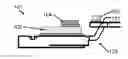
FIG. 3 shows an alternative arrangement 101 of the multiple die arrangement. The same reference numerals have been used for like parts but with the addition of “100” to the number used in FIGS. 1 and 2. FIG. 4 shows a side view of the embodiment of FIG. 3. In this arrangement a lead frame 120 is shown mounted to the base die 102. The lead frame includes lead fingers for providing an external electrical connection to the die arrangement 101. In particular, the lead frame includes three lead fingers; a first lead finger 121, a second lead finger 122 and a third lead linger 123. The lead fingers provide for connection of the terminals of the semiconductor devices on the dies 102, 103, 104 to circuitry external to the arrangement 101.
The first and third lead fingers 121 and 123 are substantially T-shaped (although could be L-shaped) and include a wider, head portion 124 and 125 respectively adjacent the base die 101 and a narrower portion 126, 127. The wider portions 124, 125 may be configured to be encapsulated within a package and the narrower portions 126, 127 may extend from the package.
In this arrangement 101, the second die 103 is mounted on the lead finger 121 and, in particular, the wider portion 124 thereof. The second die may be attached by conductive die attach material, such as solder. The wider portion of a lead finger, where it meets the remainder of the leadframe, is an advantageous point to mount a die. A bondwire 125 connects the second die 103 to the gate terminal 106 of the triac 105 of the base die 102. To obtain the same functionality as the arrangement 1 in FIG. 1, the second die 103 is mounted the opposite way up. In particular, the anode terminal 129 of the diode 110 is mounted facing upwards from the lead finger such that an electrical connection can be formed between it and the gate terminal 106. This may be achieved by providing the second die 103 with the reverse N-type and P-type diffusion arrangement compared to that provided in the example of FIG. 1. Thus, where in FIG. 1, the diode had a lower P-type diffusion and an upper N-type diffusion (such that the P-type diffusion formed the anode terminal which contacted the gate terminal 6 of the triac 5), the arrangement 101 has a upper P-type diffusion and a lower N-type diffusion, such that a bondwire can connect the P-type diffusion region to the gate terminal 6.
The third die 104 is stacked on the base die 2 as in the example of FIG. 1 and secured by die attach material or solder for example. A second bondwire 128 electrically connects the second anode terminal 13 of the thyristor 12 of third die 104 to the first lead finger 121. A third bondwire 130 connects the first anode 107 of the triac 105 to the third lead finger 123.
The arrangement 101 may comprise a temperature and overload protected Triac.
The examples herein show a diode as comprising an electronic device, formed in a die, suitable for lead finger mounting. However, other devices may be lead finger mounted. For example, two or more terminal devices wherein two of the terminals are formed on opposite sides of the die are suitable. Alternatively, dies having all terminals on one side may be mounted to the lead finger by their non-terminal side.
FIG. 5 shows a further example of a die arrangement 201. The arrangement comprises a first die 202 and a second die 203. The first die 202 includes a semiconductor device formed therein having, for example, two terminals on its upper surface; a first terminal 206 and a second terminal 207. The first die 202 is itself stacked upon a base die (not visible) which is mounted to a lead frame 220. The lead frame includes three lead fingers; a first lead finger 221, a second lead finger 222 and a third lead linger 223. The lead fingers provide for connection of the terminals of the semiconductor devices on the dies 202, 203 to circuitry external to the arrangement 201.
The second die 203 is mounted to one of the lead fingers 221 and a bondwire 225 electrically connects the semiconductor device of the second die 203 to one of the terminals 206, 207 of the first die 202. In this example, even though there is only one die (the second die 203) to be mounted in the same plane, the die 203 has been mounted on the lead finger 221. In this example, the second terminal 207 to which the second die is electrically connected, has an area smaller than the second die 203. Thus, it is more convenient to mount the second die to the lead finger 221. It will be appreciated that it may be more convenient to fabricate a second die with an area greater than the terminal on which it is to be mounted and therefore mounting the larger second die on the lead finger makes such an arrangement possible. The skilled man will realise that reasons other than area mismatch may lead to lead finger mounting being preferable, such as isolation between semiconductor devices among others. A further bondwire 228 connects the first terminal 206 of the first die 202 to the third lead finger 223.
Claims
1. A semiconductor die arrangement comprising
a first die including at least one semiconductor device;
a second die including at least one semiconductor device;
a lead frame associated with the first die and comprising one or more lead fingers,
wherein the second die is mounted on the or one of the lead fingers and electrically connected to a further element by a bond wire.
2. A semiconductor die arrangement according to claim 1, in which the further element comprises a terminal of the semiconductor device of the first die.
3. A semiconductor die arrangement according to claim 1, in which the further element comprises a terminal of a further die stacked upon the first die.
4. A semiconductor die arrangement according to claim 1, in which the semiconductor device of the second die comprises a first terminal and a second terminal on opposed sides of the die, the first terminal electrically connected to the lead finger and the second terminal electrically connected to the further element by the bondwire.
5. A semiconductor die arrangement according to claim 1, in which the arrangement comprises a third die including at least one semiconductor device, the third die mounted on the first die in a stacked configuration and electrically connected to the semiconductor device of the first die.
6. A semiconductor die arrangement according to claim 5, in which a terminal of the semiconductor device of the third die is electrically connected to a terminal of the semiconductor device of the first die by conductive die attach material.
7. A semiconductor die arrangement according to claim 4, in which the first terminal of the second die is electrically connected to the lead finger by conductive die attach material.
8. A semiconductor die arrangement according to claim 5, in which the semiconductor device of the first die comprises a triac having a gate terminal and two anode terminals; and
the semiconductor device of the second die comprises a diode having a first terminal and a second terminal, the first terminal electrically connected to the lead finger; and
the semiconductor device of the third die comprises a thyristor or silicon-controlled rectifier (SCR) stacked upon and electrically connected to one of the two anode terminals of the triac;
wherein a bondwire electrically connects the gate terminal of the triac to the second terminal of the diode.
9. A semiconductor die arrangement according to claim 6, in which a terminal of the semiconductor device of the third die is electrically connected by a bond wire to the lead finger.
10. A semiconductor die arrangement according to claim 1, in which the first die includes a first surface which mounts directly or indirectly to the leadframe and a second, opposed surface, the second surface including a first terminal and a second terminal, the first terminal having a smaller area than the second terminal, wherein the second die is electrically connected to the smaller, first terminal of the first die by a bond wire.
11. A semiconductor die arrangement according to claim 1, in which the lead finger comprises a wider portion adjacent the first die and a narrower portion for providing an external connection to the die arrangement, wherein the second die is mounted to the wider portion.
12. A method of fabricating a semiconductor die arrangement comprising;
receiving a first die including at least one semiconductor device;
receiving a second die including at least one semiconductor device;
mounting the first die to a lead frame, the lead frame comprising one or more lead fingers,
mounting the second die on one of the lead fingers; and
electrically connecting the semiconductor device of the second die to a further element by a bond wire.
13. The method according to claim 12, in which the first die includes, on the same surface, a first terminal and a second terminal, the first terminal having a smaller area than the second terminal; wherein
the step of electrically connecting comprises electrically connecting the semiconductor device of the second die to the smaller, first terminal of the first die by a bond wire; and
the method include the step of mounting a third die on the second, larger area, terminal of the first die in a stacked configuration.
14. An integrated circuit package encapsulating the semiconductor die arrangement according to claim 1.
15. An electronic device including the integrated circuit package of claim 14.
Images & Drawings included:
Sources:
- United States Patent and Trademark Office - verify current appl. status at the USPTO↗
Similar patent applications:
- » 20220179950
FINGERPRINTING OF SEMICONDUCTOR DIE ARRANGEMENTS - » 20240297148
POWER MODULE WITH IMPROVED SEMICONDUCTOR DIE ARRANGEMENT FOR ACTIVE CLAMPING - » 20140138841
Integrated circuit, a semiconductor die arrangement and a method for manufacturing an integrated circuit - » 10370435
Adhesive die attachment method for a semiconductor die and arrangement for carrying out the method - » 20210167195
Vertical power semiconductor device, semiconductor wafer or bare-die arrangement, carrier, and method of manufacturing a vertical power semiconductor device - » 20120025396
Semiconductor device with die stack arrangement including staggered die and efficient wire bonding - » 20090294977
SEMICONDUCTOR DIE AND BOND PAD ARRANGEMENT METHOD THEREOF - » 20130207280
Semiconductor device with die stack arrangement including staggered die and efficient wire bonding - » 14271792
Bonding pad arrangment design for multi-die semiconductor package structure - » 20070051949
Method and arrangment for testing a stacked die semiconductor device
Recent applications in this class:
- » 20250266329 2025-08-21
SENSOR SEMICONDUCTOR PACKAGE, ARTICLE COMPRISING THE SAME AND MANUFACTURING METHOD THEREOF - » 20250259916 2025-08-14
PACKAGE STRUCTURE - » 20250210471 2025-06-26
SEMICONDUCTOR CHIP PACKAGING DEFECT FREE DIMPLE PROCESS AND DEVICE - » 20250183124 2025-06-05
MICROELECTRONIC PACKAGE WITH RAISED CONNECTOR FOR EXTERNAL COMPONENT - » 20250125227 2025-04-17
POWER MODULE AND RELATED METHODS - » 20250112126 2025-04-03
WIDE BANDGAP POWER DEVICES WITH LOW POWER LOOP INDUCTANCE - » 20250105102 2025-03-27
POWER SEMICONDUCTOR DEVICE HAVING A SOLDER BLEED OUT PREVENTION LAYER AND METHOD FOR FABRICATING THE SAME - » 20250079267 2025-03-06
CHIP PACKAGE STRUCTURE - » 20250029900 2025-01-23
GLASS CORE PACKAGE SUBSTRATES - » 20250006596 2025-01-02
QFN PACKAGED SEMICONDUCTOR DEVICE AND METHOD OF MAKING THEREOF
Recent applications for this Assignee:
- » 20250190319 2025-06-12
METHOD AND SYSTEM TO DELAY A RESPONSE ASSOCIATED WITH A BUS TRANSACTION THAT IS TRANSMITTED TO A BUS MASTER TO PERFORM FAULT TESTING - » 20250165739 2025-05-22
RADIO FREQUENCY VOLTAGE LIMITER FOR AN RFID TRANSPONDER - » 20250119329 2025-04-10
METHOD AND DEVICE FOR DETECTING PROXIMITY OF AN EXTERNAL RF FIELD DURING ONGOING RF ACTIVITY OF THE DEVICE - » 20250119118 2025-04-10
TRANSFORMER FILTER WITH NOTCH - » 20250085344 2025-03-13
APPARATUSES AND METHODS FOR FACILIATATING A DYNAMIC CLOCK FREQUENCY FOR AT-SPEED TESTING - » 20250080342 2025-03-06
LOW-MEMORY MASKED DILITHIUM WITH ALTERNATIVE SIGNING ALGORITHM - » 20250077108 2025-03-06
Method for proving erasure of a memory - » 20250061239 2025-02-20
METHODS AND SYSTEMS FOR MULTI-MODAL SECURITY ACCESS CONTROL BASED ON DETAILS OF SECURITY CIRCUMSTANCES - » 20250023475 2025-01-16
SWITCHING REGULATOR - » 20250015814 2025-01-09
INTER-SYMBOL INTERFERENCE COMPENSATION FOR ANALOG-TO-DIGITAL CONVERTER