Integrated system of an electronic module and conductive fabric and method of making the same
US20160183367A1
2016-06-23
14/574,944
2014-12-18
✅ Patent granted
US 10,201,080 B2
2019-02-05
-
-
Binh B Tran
Volpe and Koenig, P.C.
2035-11-09
Abstract:
An electronic module assembly and method of assembling an electronic module to a conductive fabric are provided. An electronic module assembly comprises a non-conductive fabric and a conductive fabric covering at least part of a first side of the non-conductive fabric. An electronics module is disposed on the conductive fabric, and a portion of the electronics module includes a wall defining a through hole. A fastener passing through the through hole and passing through the conductive fabric is configured to electronically couple the electronics module to the conductive fabric.
Inventors:
- Murad Kurwa 58 🇺🇸 San Jose, CA, United States
- Weifeng Liu 43 🇺🇸 Dublin, CA, United States
- Anwar Mohammed 52 🇺🇸 San Jose, CA, United States
Assignee:
- Flextronics AP, LLC 328 🇺🇸 Broomfield, CO, United States
- Flextronics AP. LLC 294 🇺🇸 San Jose, CA, United States
Applicant:
Interested in similar patents?
Get notified when new applications in this technology area are published.
Classification:
H05K1/038 » CPC main
Printed circuits; Details; Use of materials for the substrate Textiles
H05K1/038 » CPC main
Printed circuits; Details; Use of materials for the substrate Textiles
H05K1/18 IPC
Printed circuits Printed circuits structurally associated with non-printed electric components
H05K1/18 IPC
Printed circuits Printed circuits structurally associated with non-printed electric components
H05K1/115 » CPC further
Printed circuits; Details; Printed elements for providing electric connections to or between printed circuits Via connections; Lands around holes or via connections
H05K1/115 » CPC further
Printed circuits; Details; Printed elements for providing electric connections to or between printed circuits Via connections; Lands around holes or via connections
H05K1/181 » CPC further
Printed circuits; Printed circuits structurally associated with non-printed electric components associated with surface mounted components
H05K1/181 » CPC further
Printed circuits; Printed circuits structurally associated with non-printed electric components associated with surface mounted components
H05K1/03 IPC
Printed circuits; Details Use of materials for the substrate
H05K1/03 IPC
Printed circuits; Details Use of materials for the substrate
H05K1/11 IPC
Printed circuits; Details Printed elements for providing electric connections to or between printed circuits
H05K1/11 IPC
Printed circuits; Details Printed elements for providing electric connections to or between printed circuits
H05K1/09 » CPC further
Printed circuits; Details Use of materials for the conductive, e.g. metallic pattern
H05K1/09 » CPC further
Printed circuits; Details Use of materials for the conductive, e.g. metallic pattern
H05K3/10 » CPC further
Apparatus or processes for manufacturing printed circuits in which conductive material is applied to the insulating support in such a manner as to form the desired conductive pattern
H05K3/10 » CPC further
Apparatus or processes for manufacturing printed circuits in which conductive material is applied to the insulating support in such a manner as to form the desired conductive pattern
H02K1/18 IPC
Details of the magnetic circuit characterised by the shape, form or construction; Stationary parts of the magnetic circuit Means for mounting or fastening magnetic stationary parts on to, or to, the stator structures
H05K9/009 » CPC further
Screening of apparatus or components against electric or magnetic fields; Shielding materials; Electromagnetic shielding materials, e.g. EMI, RFI shielding comprising electro-conductive fibres, e.g. metal fibres, carbon fibres, metallised textile fibres, electro-conductive mesh, woven, non-woven mat, fleece, cross-linked
H05K1/0283 » CPC further
Printed circuits; Details; Bendability or stretchability details Stretchable printed circuits
H05K1/0283 » CPC further
Printed circuits; Details; Bendability or stretchability details Stretchable printed circuits
H05K1/0366 » CPC further
Printed circuits; Details; Use of materials for the substrate; Organic insulating material consisting of two or more materials, e.g. two or more polymers, polymer + filler, + reinforcement reinforced, e.g. by fibres, fabrics
H05K1/0366 » CPC further
Printed circuits; Details; Use of materials for the substrate; Organic insulating material consisting of two or more materials, e.g. two or more polymers, polymer + filler, + reinforcement reinforced, e.g. by fibres, fabrics
H05K1/0373 » CPC further
Printed circuits; Details; Use of materials for the substrate; Organic insulating material consisting of two or more materials, e.g. two or more polymers, polymer + filler, + reinforcement containing additives, e.g. fillers
H05K1/0373 » CPC further
Printed circuits; Details; Use of materials for the substrate; Organic insulating material consisting of two or more materials, e.g. two or more polymers, polymer + filler, + reinforcement containing additives, e.g. fillers
H05K1/113 » CPC further
Printed circuits; Details; Printed elements for providing electric connections to or between printed circuits; Pads for surface mounting, e.g. lay-out directly combined with via connections Via provided in pad; Pad over filled via
H05K1/113 » CPC further
Printed circuits; Details; Printed elements for providing electric connections to or between printed circuits; Pads for surface mounting, e.g. lay-out directly combined with via connections Via provided in pad; Pad over filled via
H05K2201/05 » CPC further
Indexing scheme relating to printed circuits covered by Flexible printed circuits [FPCs]
H05K2201/05 » CPC further
Indexing scheme relating to printed circuits covered by Flexible printed circuits [FPCs]
H05K2201/0959 » CPC further
Indexing scheme relating to printed circuits covered by; Shape and layout; Shape and layout details of conductors; Conductive through-holes or vias Plated through-holes or plated blind vias filled with insulating material
H05K2201/0959 » CPC further
Indexing scheme relating to printed circuits covered by; Shape and layout; Shape and layout details of conductors; Conductive through-holes or vias Plated through-holes or plated blind vias filled with insulating material
H05K2201/10242 » CPC further
Indexing scheme relating to printed circuits covered by; Details of components or other objects attached to or integrated in a printed circuit board; Other objects, e.g. metallic pieces Metallic cylinders
H05K2201/10242 » CPC further
Indexing scheme relating to printed circuits covered by; Details of components or other objects attached to or integrated in a printed circuit board; Other objects, e.g. metallic pieces Metallic cylinders
H05K2201/10295 » CPC further
Indexing scheme relating to printed circuits covered by; Details of components or other objects attached to or integrated in a printed circuit board; Other objects, e.g. metallic pieces Metallic connector elements partly mounted in a hole of the PCB
H05K2201/10295 » CPC further
Indexing scheme relating to printed circuits covered by; Details of components or other objects attached to or integrated in a printed circuit board; Other objects, e.g. metallic pieces Metallic connector elements partly mounted in a hole of the PCB
H05K1/00 IPC
Printed circuits
H05K1/00 IPC
Printed circuits
H05K3/32 » CPC further
Apparatus or processes for manufacturing printed circuits; Assembling printed circuits with electric components, e.g. with resistor electrically connecting electric components or wires to printed circuits
H05K3/32 » CPC further
Apparatus or processes for manufacturing printed circuits; Assembling printed circuits with electric components, e.g. with resistor electrically connecting electric components or wires to printed circuits
H05K9/00 IPC
Screening of apparatus or components against electric or magnetic fields
H05K9/00 IPC
Screening of apparatus or components against electric or magnetic fields
H05K1/02 IPC
Printed circuits Details
H05K1/02 IPC
Printed circuits Details
H05K3/42 » CPC further
Apparatus or processes for manufacturing printed circuits; Forming printed elements for providing electric connections to or between printed circuits Plated through-holes or plated via connections
H05K3/42 » CPC further
Apparatus or processes for manufacturing printed circuits; Forming printed elements for providing electric connections to or between printed circuits Plated through-holes or plated via connections
H05K2201/10303 » CPC further
Indexing scheme relating to printed circuits covered by; Details of components or other objects attached to or integrated in a printed circuit board; Other objects, e.g. metallic pieces; Metallic connector elements partly mounted in a hole of the PCB Pin-in-hole mounted pins
Description
FIELD OF INVENTION
Embodiments of the present disclosure generally relate to an electronic module assembled to a conductive fabric, and a method of assembling an electronic module to a conductive fabric.
BACKGROUND
In some applications, it may be desirable to form an assembly of an electronic module on a conductive fabric to form an integrated system. Conventional assemblies include modules stitched to a conductive fabric using conductive wire. Stitching is an intensive manual process not suitable for high volume or automation. In some stitched assemblies, the stitches become loose as the fabric flexes. It has also been noted that some conductive fabrics are not well suited for joining techniques requiring elevated temperatures.
Accordingly, a need exists for an improved electronic module assembly and method of assembling an electronic module to a conductive fabric.
SUMMARY
Embodiments of an electronic module assembly and method of assembling an electronic module to a conductive fabric are provided herein. In an embodiment, an electronic module assembly comprises a non-conductive fabric and a conductive fabric covering at least part of a first side of the non-conductive fabric. An electronics module is disposed on the conductive fabric, and a portion of the electronics module includes a wall defining a through hole. A fastener passing through the through hole and passing through the conductive fabric is configured to electronically couple the electronics module to the conductive fabric.
In an embodiment, a method of making an electronics assembly comprising an electronics module and a conductive fabric is disclosed. The method comprises forming a substrate including a conductive fabric covering at least part of a first side of a non-conductive fabric; disposing an electronics module having one or more through holes on the substrate with the through holes aligned with a portion of the conductive fabric; inserting a fastener to pass through the through hole and through the substrate; and clamping the module to the substrate to form an electrical connection using the fastener.
Other and further embodiments of the present invention are described below.
BRIEF DESCRIPTION OF THE DRAWINGS
Embodiments of the present invention, briefly summarized above and discussed in greater detail below, can be understood by reference to the illustrative embodiments of the invention depicted in the appended drawings. It is to be noted, however, that the appended drawings illustrate only typical embodiments of this invention and are therefore not to be considered limiting of its scope, for the invention may admit to other equally effective embodiments.
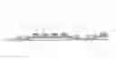
FIG. 1 depicts a side sectional view of an electronics module assembly in accordance with an embodiment of this disclosure.
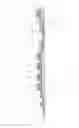
FIG. 2 is a side sectional view of an electronics module assembly in accordance with an embodiment of this disclosure.
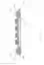
FIG. 3 is a flow diagram in accordance with an embodiment of a method of this disclosure.
DETAILED DESCRIPTION
Certain terminology is used in the following description for convenience only and is not limiting. “Conductive” is used to mean “electrically conductive” unless the context clearly calls for a different definition. Conversely, “non-conductive” means resistant to electrical conduction, or an electrical insulator. The words “front,” “rear,” “upper” and “lower” designate directions in the drawings to which reference is made. A reference to a list of items that are cited as “at least one of a, b, or c” (where a, b, and c represent the items being listed) means any single one of the items a, b, or c, or combinations thereof. The terminology includes the words specifically noted above, derivatives thereof and words of similar import.
FIG. 1 depicts a side sectional view of an electronics module assembly 100 comprising a substrate 102 including a non-conductive fabric 104, a conductive fabric 110, and an electronics module 116 (one electronics module and a partial are shown in FIG. 1). The non-conductive fabric 104 has a first side 106 and a second side 108 opposite and generally parallel with the first side 106. The conductive fabric 110 covers at least a part of the first side 106 and may be attached to the non-conductive fabric 104 using one or more of stitching or gluing. If stitching is used, the thread used to attach the conductive fabric 110 to the non-conductive fabric 104 is preferably a non-conductive thread 112, for example a thread formed from, in non-limiting examples, natural fibers such as cotton, or synthetic fibers such as polyester or nylon. If gluing is used, the glue 114, or adhesive, is preferably non-conductive.
An electronics module 116 is positioned on the substrate 102 so that a portion of the module 116 is disposed on the conductive fabric 110 with a bottom surface 126 of the module 116 adjacent to the conductive fabric 110 and a top surface 128 spaced apart from the conductive fabric 110. The portion 118 disposed on the conductive fabric 110 includes an interior wall 120 that defines a through hole 122 formed through the portion 118. In some embodiments, the wall 120 is plated with a conductive material 124 which may include, in non-limiting examples, silver, gold over nickel, or tin. The bottom surface 126 and the top surface 128 at least partially surrounding the through hole 122 is preferably includes conductive elements 130a, 130b, for example copper pads which may be plated with silver, gold, or nickel.
The electronics module 116 may include, in non-limiting examples, sensors 116a, light sources such as light emitting diodes (LEDs) 116b, recording devices 116c, displays 116d, and the like. Other electronic devices can be included in the electronics module 116 within the scope and spirit of this disclosure.
As shown in FIG. 2, a fastener 202 is used to clamp the electronics module 116 to the substrate 102 to form an electrical connection between the module and the substrate. In the non-limiting embodiment of FIG. 2, a stem 204 of fastener 202 passes through the through hole 122, penetrates and passes through the conductive fabric 110 and the non-conductive fabric 104 and exits through the second side 108 of the non-conductive fabric 104. In an embodiment, the conductive and non-conductive fabrics 110, 104 may have preformed holes to allow passage of the fastener 202. In another embodiment, the fastener 202 may pierce one or both of the conductive and non-conductive fabrics 110, 104, forming an opening therein.
As shown in FIG. 2, a first end of the fastener 202 has a head 206 larger than the through hole 122 formed in the electronics module 116. The head 206 is configured to contact the conductive elements 130a formed on the top surface 128 of the electronics module 116. In an embodiment, the second end of the fastener 202 is adapted to accept a mating element 208 to facilitate the clamping. For example, the second end of the fastener 202 may include an external thread and the mating element 208 may have a corresponding internal thread to engage the external thread and advance along the length of the stem 204 when rotated.
In another embodiment, the second end of the fastener 202 may be subjected to a compressive load to facilitate clamping. During application of the compressive load, the second end of the fastener 202 may be deformed by the pressure and expand so that the second end becomes larger than the through hole 122.
The fastener 202 is a conductive element formed from an electrically conductive material, for example metal, or from a non-conductive material that is plated with a conductive material. When the electronics module 116 is clamped to the substrate 102, the fastener 202 forms an electrical connection between the electronics module 116 and the conductive fabric 110. The fastener 202 forms a gas-tight connection between the electronics module 116 and the conductive fabric 110.
The inventors have noted that the disclosed electronics module assembly 100 may provide a durable electrical connection between an electronics module 116, which may be flexible or rigid, and a flexible substrate 102 formed from a conductive fabric 110 and a non-conductive fabric 104. The disclosed assembly may be well-suited for manual or automated assembly, for example using the method 300 of FIG. 3.
At 302, a substrate 102 is formed from a conductive fabric 110 covering at least part of a first side of a non-conductive fabric 104. The conductive fabric 110 may be attached to the non-conductive fabric using one or more of stitching or gluing. The attachment may be accomplished using non-conductive thread for stitching or a non-conductive glue or adhesive for gluing.
At 304, an electronics module 116 is disposed on the substrate 102. The module 116 includes one or more through holes 122 formed though a portion of the module 116. When electronics module 116 is disposed on the substrate 102, the through hole 122 is placed upon, or aligned with, a portion of the conductive fabric 110.
At 306, a fastener is inserted to pass through the through hole 122 in the electronics module 116 and to pass through the substrate 102. One or both of the conductive fabric 110 and the non-conductive fabric 104 may have a preformed hole formed therein to accept the fastener 202.
At 208, the electronics module 116 is clamped to the substrate 102 to form an electrical connection using the fastener 202.
Thus an electronics module assembly and method of assembling an electronic module to a conductive fabric are provided herein. The inventive module may advantageously provide a durable electrical connection between an electronics module and a substrate. The inventive method may facilitate manual or automated assembly of an electronics module to a substrate with increased reliability, thereby improving production throughput.
Having thus described the present invention in detail, it is to be appreciated and will be apparent to those skilled in the art that many physical changes, only a few of which are exemplified in the detailed description of the invention, could be made without altering the inventive concepts and principles embodied therein. It is also to be appreciated that numerous embodiments incorporating only part of the preferred embodiment are possible which do not alter, with respect to those parts, the inventive concepts and principles embodied therein. The present embodiment and optional configurations are therefore to be considered in all respects as exemplary and/or illustrative and not restrictive, the scope of the invention being indicated by the appended claims rather than by the foregoing description, and all alternate embodiments and changes to this embodiment which come within the meaning and range of equivalency of said claims are therefore to be embraced therein.
Claims
What is claimed is:1. An electronic module assembly comprising:
a non-conductive fabric;
a conductive fabric covering at least part of a first side of the non-conductive fabric;
an electronics module disposed on the conductive fabric, a portion of the electronics module includes a wall defining a through hole; and
a fastener passing through the through hole and passing through the conductive fabric,
wherein the fastener is configured to electronically couple the electronics module to the conductive fabric.
2. The module of claim 1, wherein the wall is plated with a conductive material.
3. The module of claim 1, wherein the portion of the electronics module comprises a top surface and a bottom surface surrounding the through hole, a portion of the top surface and bottom surface is plated with a conductive material.
4. The module of claim 1, wherein the conductive fabric is attached to the non-conductive fabric substrate using one or more of stitching or gluing.
5. The module of claim 1, wherein the fastener is a metal fastener.
6. The module of claim 1, wherein the fastener includes a metal coating.
7. The module of claim 1, wherein the conductive fabric is formed from a metal plated yarn.
8. A method of making an electronics assembly comprising an electronics module and a conductive fabric, comprising:
forming a substrate including a conductive fabric covering at least part of a first side of a non-conductive fabric;
disposing an electronics module having one or more through holes on the substrate with the through holes aligned with a portion of the conductive fabric;
inserting a fastener to pass through the through hole and through the substrate; and
clamping the module to the substrate to form an electrical connection using the fastener.
9. The method of claim 8, wherein forming the substrate includes:
attaching the conductive fabric to the non-conductive fabric using one or more of stitching or gluing.
10. The method of claim 8, wherein the clamping forms a gas tight connection between the module and the conductive fabric.
Images & Drawings included:

Sources:
- United States Patent and Trademark Office - verify current appl. status at the USPTO↗
Recent applications in this class:
- » 20250240885 2025-07-24
FABRIC TOUCH PANEL - » 20250234458 2025-07-17
METAL-CLAD LAMINATE, PRINTED WIRING BOARD, SEMICONDUCTOR PACKAGE, AND METHOD FOR MANUFACTURING SAME - » 20250176101 2025-05-29
BONDING STRUCTURE IN ELECTRICALLY CONDUCTIVE PATTERN OF FABRIC - » 20250063654 2025-02-20
STRETCHABLE, FABRIC SENSOR, WEARABLE ELECTRONIC DEVICE INCLUDING THE SAME, AND METHOD OF MAKING THE SAME - » 20240414840 2024-12-12
GLASS CLOTH, PREPREG AND PRINTED WIRING BOARD - » 20240244744 2024-07-18
PRINTED WIRING BOARD AND METHOD FOR MANUFACTURING PRINTED WIRING BOARD - » 20240196527 2024-06-13
METHOD FOR MANUFACTURING LASER-INDUCED GRAPHENE BASED E-TEXTILE AND LASER SYSTEM IMPLEMENTING THE METHOD - » 20240188213 2024-06-06
CIRCUIT BOARD FOR A CONTROL DEVICE OF A VEHICLE, AND METHOD FOR MANUFACTURING OF SUCH A CIRCUIT BOARD - » 20240080975 2024-03-07
CIRCULAR MANUFACTURING OF TEXTILE-BASED SENSORS - » 20230354516 2023-11-02
CONNECTORS FOR INTEGRATING CONDUCTIVE THREADS TO NON-COMPATIBLE ELECTROMECHANICAL DEVICES
Recent applications for this Assignee:
- » 20250170022 2025-05-29
FLUIDIC ANALYSIS AND CONTROL THROUGH IMAGE PROCESSING - » 20250119718 2025-04-10
NOVEL BLUETOOTH RADIO ARCHITECTURE FOR IMPROVED DATA TRANSFER FROM MEDICAL DEVICES - » 20250116919 2025-04-10
DEVICE FOR ASSISTING A DRIVER - » 20250115124 2025-04-10
SYSTEM FOR ASSISTING A DRIVER - » 20250018123 2025-01-16
LEADSCREW TIP FOR AN AUTOINJECTOR - » 20250018115 2025-01-16
BIO-ELECTRICAL SENSING IN AN AUTOINJECTOR - » 20240350741 2024-10-24
FORCE SENSOR FOR MEDICAL DEVICES - » 20240277942 2024-08-22
ELECTROMECHANICAL ARCHITECTURE FOR CONNECTED PREFILLED DISPOSABLE SYRINGES - » 20230012795 2023-01-19
Systems and methods for providing social media with an intelligent television - » 20220317777 2022-10-06
LIBRARY AND RESOURCES FOR THIRD PARTY APPS FOR SMART TV