Approach for an area-efficient and scalable CMOS performance based on advanced Silicon-On-Insulator (SOI), Silicon-On-Sapphire (SOS) and Silicon-On-Nothing (SON) technologies
US20170040461A1
2017-02-09
14/821,685
2015-08-07
✅ Patent granted
US 9,741,857 B2
2017-08-22
-
-
Michael Zarroli
2035-08-07
Abstract:
The invention provides the guided design approach to optimize the device performance for a best area-efficient layout footprint in a single-leg MOS device that is based on any of the SOI, SOS or SON technologies. The design methodology depends on a new proprietary device architecture that is also being claimed in this patent and that allows the implementations of the design equations of our methodology.
Applicant:
Interested in similar patents?
Get notified when new applications in this technology area are published.
Classification:
H01L29/7838 » CPC further
Semiconductor devices adapted for rectifying, amplifying, oscillating or switching, or capacitors or resistors with at least one potential-jump barrier or surface barrier, e.g. PN junction depletion layer or carrier concentration layer; Details of semiconductor bodies or of electrodes thereof; Multistep manufacturing processes therefor; Types of semiconductor device ; Multistep manufacturing processes therefor controllable by only the electric current supplied, or only the electric potential applied, to an electrode which does not carry the current to be rectified, amplified or switched; Unipolar devices, e.g. field effect transistors; Field effect transistors with field effect produced by an insulated gate without inversion channel, e.g. buried channel lateral MISFETs, normally-on lateral MISFETs, depletion-mode lateral MISFETs
H01L29/786 IPC
Semiconductor devices adapted for rectifying, amplifying, oscillating or switching, or capacitors or resistors with at least one potential-jump barrier or surface barrier, e.g. PN junction depletion layer or carrier concentration layer; Details of semiconductor bodies or of electrodes thereof; Multistep manufacturing processes therefor; Types of semiconductor device ; Multistep manufacturing processes therefor controllable by only the electric current supplied, or only the electric potential applied, to an electrode which does not carry the current to be rectified, amplified or switched; Unipolar devices, e.g. field effect transistors; Field effect transistors with field effect produced by an insulated gate Thin film transistors, i.e. transistors with a channel being at least partly a thin film
H01L29/78 IPC
Semiconductor devices adapted for rectifying, amplifying, oscillating or switching, or capacitors or resistors with at least one potential-jump barrier or surface barrier, e.g. PN junction depletion layer or carrier concentration layer; Details of semiconductor bodies or of electrodes thereof; Multistep manufacturing processes therefor; Types of semiconductor device ; Multistep manufacturing processes therefor controllable by only the electric current supplied, or only the electric potential applied, to an electrode which does not carry the current to be rectified, amplified or switched; Unipolar devices, e.g. field effect transistors; Field effect transistors with field effect produced by an insulated gate
H01L27/1203 » CPC further
Devices consisting of a plurality of semiconductor or other solid-state components formed in or on a common substrate including semiconductor components specially adapted for rectifying, oscillating, amplifying or switching and having at least one potential-jump barrier or surface barrier; including integrated passive circuit elements with at least one potential-jump barrier or surface barrier the substrate being other than a semiconductor body, e.g. an insulating body the substrate comprising an insulating body on a semiconductor body, e.g. SOI
H01L27/12 IPC
Devices consisting of a plurality of semiconductor or other solid-state components formed in or on a common substrate including semiconductor components specially adapted for rectifying, oscillating, amplifying or switching and having at least one potential-jump barrier or surface barrier; including integrated passive circuit elements with at least one potential-jump barrier or surface barrier the substrate being other than a semiconductor body, e.g. an insulating body
Description
INDEX TERMS
-
- CMOS: Complimentary-Metal-Oxide-Semiconductor.
- MOS: Metal-Oxide-Semiconductor.
- NMOS: N-channel MOS.
- PMOS: P-channel MOS.
- SOI: Silicon-On-Insulator.
- SOS: Silicon-On-Sapphire.
- SON: Silicon-On-Nothing.
- PD: Partially-Depleted.
- FD: Fully-Depleted.
- BTS: Body-Tied-Source.
- FBE: Floating-Body-Effect.
- RF: Radio-Frequency.
REFERENCE TO SEQUENCE LISTING
Other Publications
- [1]. Randy Wolf, Dawn Wang, Alvin Joseph, Alan Botula, Peter Rabbeni, David Harame and Jim Dunn, “Highly Resistive Substrate CMOS on SOI for Wireless Front-End Switch Application”, CS MANTECH Conference, May 16-19, 2011, Palm Springs, Calif., USA.
- [2]. Cui Jie, Chen Lei, Zhao Peng, Niu Xu, and Liu Yi, “A linear 180 nm SOI CMOS antenna switch module using integrated passive device filters for cellular applications”, Journal of Semiconductors, vo. 35, no. 6, June 2014.
- [3]. Matteo Maria Vignetti, Michael Salter, Duncan Platt, Anders Hallen, “Thermal Simulations and Design Guidelines on Multi-Finger Pas based on 28 nm FD-SOI Technology”, A Master Thesis, School of Information And Communication Technology, KUNGLIGA TEKNISKA HOGSKOLAN, June 2013.
- [4]. Lorenzo Bertolissi, Ing. Luca Selmi, Gerhard Knoblinger, Pierpaolo Palestri, David Esseni, “Modeling and Simulation of Self-Heating Effects in Deep Sub-Micron Silicon (SOI) Technologies for Analog Circuits”, A Thesis, Department of Electrical Engineering, Universita Degli Studi Di Udine, 2004.
- [5]. Vandana B., “Study of Floating Body Effect in SOI Technology”, International Journal of Modern Engineering Research, vo. 3, iss. 3, May-June 2013.
- [6]. Franklin L. Duan et al., “LDD design tradeoffs for single transistor latch-up and hot carrier degradation control in accumulation mode FD SOI MOSFETs”, IEEE Trans. on Elec. Dev., vo. 44, no. 6, 1997.
- [7]. Ted Johansson, Senior Member IEEE, and Jonas Fritzin, Member IEEE, “A Review of Watt-level CMOS RF power amplifiers”, IEEE Trans. on Microwave Theory and Techniques, vo. 62, iss. 1, 2013
- [8]. X. Gu, H. Wang, T. L. Chen and G. Gildenblat, “Substrate Current in Surface-Potential-Based Compact MOSFET”, Nanotech, vo. 2, 2003.
- [9]. Costa J., Carrol M., Jorgenson J., Mckay T., Ivanov T., Dinh T., Kozuch D., Remoundos G., Kerr D., Tombak A., Mcmaken J., Zybura M., “A Silicon RFCMOS SOI Technology for Integrated Cellular/WLAN RF TX Modules”, IEEE/MIT-S International Microwave Symposium, June 2007.
- [10]. Jean-Pierre Colinge, “Multiple-gate SOI MOSFETs”, Soild-State Electronics, vo. 48, pp. 897-905, 2004.
- [11]. Kwangseok Han, Jeong-hu Han, Minkyu J E and Hyungcheol Shin, “RF Characteristics of 0.18-μm CMOS Transistors”, Journal of the Korean Physical Society, vo. 40, no. 1, pp. 45-48, January 2002.
- [12]. Abraham Yoo, “Design, Implementation, Modeling, and Optimization of Next Generation Low-Voltage Power MOSFETs”, A thesis, Department of Materials Science and Engineering, University of Toronto, 2010.
- [13]. Jean-Pierre Raskin, “SOI Technology: An opportunity for RF Designers?”, invited paper, Journal of Telecommunications And Information Technology, April 2009.
- [14]. J. Borremans, B. Parvais, M. Dehan, S. Thijs, P. Wambacq, A. Mercha, M. Kuijk, G. Carchon and S. Decoutere, “Perspective of RF design in future planar and FInFET CMOS”, Radio Frequency Integrated Symposium, pp. 75-78, Atlanta Ga., 2008.
- [15]. Y. Fukunaga, M. Miura-Mattausch, U. Feldmann, H. Kikuchiharasa, M. Miyake, H. J. Mattausch and T. Nakagawa, “Compact Modeling of SOI MOSFETs with Ultra Thin Silicon and BOX Layers for Ultra low Power Applications”, 2013 International Conference On Simulation of Semiconductor Processes and Devices (SISPAD), pp. 284-287, September 2013.
- [16]. Bin Yu, Student Member IEEE, Clement H. J. Wann, Member IEEE, Edward D. Nowak, Senior Member IEEE, Kenji Noda, Member IEEE, and Chenming Hu, Fellow IEEE, “Short-Channel Effect Improved by Lateral Channel-Engineering in Deep-Submicronmeter MOSFET's”, IEEE Trans. on Electron devices, vo. 44, no. 4, April 1997.
- [17]. A. H. Tarakji, “A Novel Pseudo-Fully-Depleted-Silicon-On-Insulator (PFD-SOI) MOS Device Architecture Optimal for the High-Power Radio-Frequency Applications”, Presented at the 2015 IEEE Topical Symposium on Power Amplifiers for Wireless Communications. San Diego, Calif. September 2015.
- [18]. C. Fenouillet-Beranger, P. Perreau, P. Boulenc, L. Tosti, S. Barnola, F. Andrieu, O. Weber, R. Beneyton, C. Perrot, C. de Buttet, F. Abbate, Y. Campidelli, L. Pinzelli, P. Gouraud, A. Margain, S. Peru, K. K. Bourdelle, B. Y. Nguyen, F. Boedt, T. Poiroux, O. Faynot, T. Skotnicki, F. Boeuf, “Parasitic bipolar impact in 32 nm undoped channel Ultra-Thin BOX (UTBOX) and biased Ground Plane FD SOI high-K/metal Gate technology”, Solid-State Electronics, 74, pp. 32-37, 2012.
- [19]. J. Damiano and P. D. Franzon, “Integrated Dynamic Body Contact for H-gate P-SOI MOSFETs for High Performance/Low Power”, 2004 IEEE International SOI Conference, October 2004.
- [20]. K. Hirose, H. Saito, S. Fukuda, Y. Kuroda, S. Ishii, D. Takahashi and K. Yamamoto, “Analysis of Body-Tie-Effects on SEU Resistance of Advanced FD-SOI SRAMs Through Mixed-Mode 3-D Simulations”, IEEE Trans. on Nuclear Science, vo. 51, no. 6, December 2004.
- [21]. Arash Daghighi, Mohamed Osman, Mohamed A. Imam, “An area efficient body contact for low and high voltage SOI MOSFET devices”, Solid-State Electronics, vo. 52, pp. 196-204, 2008.
- [22]. Toshiyuki Nakamura, Hideaki Matsuhashi and Yoshiki Nagatomo, “Silicon on Sapphire (SOS) Device Technology”, Oki Technical Review, vo. 71, no. 4, iss. 200, October 2004.
- [23]. Malgorzata Jurczak, Thomas Skotnicki, Member IEEE, M. Paoli, B. Tormen, J. Martins, Jorge Luis Regolini, Didier Dutartre, Pascal Ribot, D. Lenoble, Roland Pantel and Stephanie Monfray, “Silicon-On-Nothing (SON)—an Innovative process for Advanced CMOS”, IEEE Trans. on Elec Dev., vo. 47, no. 11, November 2011.
- [24]. Vandana Kumari, Manoj Saxena, R. S. Gupta and Mridula Gupta, “Performance Investigation of Insulated Shallow Extension Silicon On Nothing (ISE-SON) MOSFET for Low Voltage Digital Applications”, Journal of Semiconductor Technology and Science, vo. 13, no. 6, December 2013.
- [25]. Ben G. Streetman, “Solid State Electronic Devices, Fourth Edition”, Prentice Hall Series, Englewood Cliffs, N.J., 1995.
- [26]. Kwyro Lee, Michael Shur, Tor A. Fjeldly and Trond Ytterdal, “Semiconductor device modeling for VLSI”, Chapter 3, pp. 188-374. Prentice-Hall, Inc. Upper Saddle River, N.J., USA, 1993.
- [27]. HYUNG-KYU LIM, Student Member IEEE and Jerry G. Fossum, Fellow IEEE, “Threshold Voltage of Thin-Film Silicon-On-Insulator (SOI) MOSFET's”, IEEE Trans. on Electron Dev. Vo. ED. 30, no. 10, October 1983.
- [28]. Weis V., Fuhrmann E., Junge A., Lutz R., Rochel M., Seider-Scmidt M., Unger R.-S, Wallace C., Kuei J., “Fast characterization of electrical fails overlaying to inline defect inspection during 90 nm copper logic technology development”, International Symposium on Semiconductor Manufacturing, Santa Clara, Calif., 2007.
- [29]. Dieter K. Schroder, “Semiconductor Material And Device Characterization”, 3rd edition, John Wiley & Sons, inc., Hoboken, N.J., 2006.
- [30]. Leland Chang, Student Member IEEE, Yang-Kyu Choi, Daewon Ha, Pushkar Ranade, Shiying Xiong, Jeffrey Bokor, Fellow IEEE, Chenming Hu, Fellow IEEE, and Tsu-Jae King, Senior Member IEEE, “Extremely Scaled Nano-CMOS Devices”, Proceedings of the IEEE., vo. 91, no. 11, November 2003.
TABLES
- TABLE 1. Process Parameters, Target Electric Specifications, and the design optimization on our fabricated FD-SOI MOSFET.
- TABLE 2. Design Equations and the “equation”-based design flow for optimization
BACKGROUND OF THE INVENTION
CMOS circuits designs based on the advanced SOI technology are continuously proving to be better match than Gallium-Arsenide (GaAs) for the compact radio-frequency building-blocks [1, 2]. SOI technology realizes speed through the suppression of Junction capacitances with Buried-Oxide film (BOX) versus the speed that can be achieved from higher carriers Mobility in the less matured GaAs technology. Additionally, this same suppression of the junction capacitances suppresses the junction leakage current and results in reduced parasitic power consumption. Yet one major obstacle, separate from the resulting low thermal conductivity that is caused from the buried insulating dielectric film [3, 4], and that is the Floating-Body-Effect (FBE) [5, 6], is still impeding the applications of this SOI-based MOS into the analog cellular RF power-amplifiers (PA's). This is primary because to achieve the typical high RF wattage that is required for cellular PA's [7], an elevated Drain biasing and a high output current are required, both increase the undesired impact-ionization current (II-current) that governs the FBE [8]. As this II-current increases the FBE becomes more and more pronounced to cause severe malfunctions and circuits failure. As a matter of fact, power-amplifiers for the cellular RF handsets based on SOI technology had rarely been demonstrated yet and are hardly being integrated or commercialized to date simply because no reliable and operational large-periphery SOI-based CMOS structures are available to date meeting the desired bandwidths and currents. One power-amplifier design based on SOI suppressed the FBE but failed to eliminate the junctions parasitics; it therefore negated in the first place all the known advantages of this SOI technology [9]. It further failed to capture desired performance above the 2 GHz. The use of multi-leg (or multi-finger) design that decomposes a large-periphery structure into dozens, hundreds or even thousands of parallel transistors of smaller Gate-widths can deliver the desired high output currents [3, 10], and can suppress the FBE due to the lower drive current per leg, however such large-periphery multi-leg design is well known to increase the parasitic Gate-to-Body capacitance [11], as well as the Gate-to-Drain and the Gate-to-Source overlap capacitances [12]. It does consequently limit the cutoff frequencies (ft and fmax), and correspondingly the RF power gain; included are multi-leg designs based on the SOI technology [13]. It was specifically demonstrated that the cutoff frequency ft did dramatically decrease with the increase of number of legs (or fingers) [6]. Furthermore, same reference also demonstrated that as the Gate-width per leg was increased, a proportional decrease of the number of legs to maintain a same output current resulted in more than 20% increase in ft; it therefore thoroughly demonstrated that a multi-leg design does considerably increase the parasitics for a same output current and does consequently reduce the RF bandwidth and the power gain. This is in addition to the fact that a multi-leg design naturally results in a larger layout area for same current drive. Separately, it was demonstrated that the use of multi-leg design based on FINFETs can further amplify this increase of parasitics and it was explicitly demonstrated that the three-dimensional nature of the FINFET architecture has huge impact on lowering the cutoff frequencies [13, 14]. A single-leg SOI FINFET with LG=40 nm showed a strong 55% reduction in its cutoff frequency from effect of extrinsic capacitances alone as compared to a planar bulk architecture of same peripheral size [13]. Therefore it is most apparent that while the FINFET appears to offer great potential to comply with the downscaling requirements of the ITRS for logic operations (Ion/Ioff), its potential for the analog RF PA's appears less promising [13].
The need for higher currents is also crucial for low insertion-loss RF-switches, and for an enhanced performance on all the analog and digital circuitries alike; such as the Phase-Locked-Loop.
Based on the above, a best approach to achieve the desired high currents for the analog RF PA modules based on SOI CMOS would be through incorporation of a planar design that is totally free of FBE and that utilizes largest possible Gate-width per leg for the purpose of minimizing the number of legs required to meet the desired output current target. The larger the Gate-width per leg, the less parallel legs are required to meet the desired output current target, and consequently the higher become the operational bandwidth and the RF power gain. The peripheral layout area for a same drive current gets also reduced.
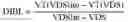
The FBE is mostly inherent to the NMOS device and it manifests itself in PD-SOI NMOS with build-up of positively charged Holes in P-Body that are generated from Impact-Ionizations at the Drain's edge of the device and which continue to accumulate with an increasing Drain Supply-voltage till they lower the barrier under the channel between P-Body and Source and start to diffuse causing an abrupt up-tick of the device current [5]. At higher Drain Supply-voltage a latch-up of the parasitic Bipolar can occur from which the device will no longer turn-off even after the Gate voltage is brought back to values lower than the threshold-voltage (VT). This up-tick of current (or the “kink-effect”, as is often referred to in technical literatures) is totally undesirable as it causes a distorted linearity of the RF power-amplifiers, a degraded overall performance, a reduced signal-to-noise ratio, and can result in false outputs from the Logic Gates. While this kink-effect can be absent in the more advanced FD-SOI NMOS, because this device operates normally with its Body/Source barrier already lowered due to the Full-Depletion of its Body, this device may still exhibit the FBE when biased in a very strong inversion mode for the highest drive current [5, 15]. Separately, and from a practical prospective, the highly doped Halo pockets underneath both edges of the Gate, and that have become a must in today's highly downscaled CMOS technology nodes to control the Off-state leakage current [16] is preventing full depletion of the entire P_Body region, and do therefore still cause the FBE when a relatively high bias is applied to Drain [17]. Furthermore, this FD-SOI MOS is more susceptible to latch-up of its built-in parasitic Bipolar structure [6, 18]; since its Body/Source barrier is already lowered, the II-current can more easily latch the parasitic Bipolar. Concrete latch-up of the parasitic Bipolar structure was evidenced in FD SOI at 3.4V and at 4V Drain biases [6, 18]. These biases are very typical to the supply voltages that are used today in the RF power PA's and other Integrated-Circuits (IC) of the cellular handsets (3.5-3.8V). The key conclusions here is that the FD-SOI MOS is still susceptible to failure at the typical supply biases that are in use today in the cellular handsets; and, that the device still appears to pose a degree of uncertainty in terms of its operational reliability at and around these supply biases unless further optimizations in design and/or in processes get undertaken. Another key conclusion is that when high bias to the Device Drain needs be applied, the fully depleted SOI device can no longer exist practically nowadays as we know it due to the simple fact that the excessively downscaled Gate-lengths in today's most advanced technology nodes, coupled with the effect of Drain-Induced-Barrier-Lowering (DIBL), necessitate the presence of highly doped Halo pockets at the both edges of the device Gate to control the Off-state power consumption [16].
Particularly most susceptive to this notorious FBE are Integrated-Circuits (ICs) that depend on the relatively high Supply-voltages (>3.3V) in their normal operating modes. This is simply due to the fact that not only the effective Gate-width of the SOI-based NMOS dictates the amount of II-current that governs the FBE, but also the magnitude of its Supply-voltage. Such ICs include the RF power amplifiers for cellular handsets that typically operate with close to al Watt of RF output power. Also susceptive are the analog IC modules such as regulators and power-management ICs.
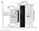
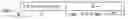
The most effective technique that is in use to date to circumvent the kink-effect and the Bipolar latch-up in a single-leg SOI MOS, is through incorporation of a Body-Tied-Source (BTS) area within the Device peripheral layout that provides a path for Holes generated from Impact-Ionization to sink-out without lowering the Body/Source barrier under the channel or forward-biasing it [19, 20, 21]. The BTS consists of highly P-doped (P+) area(s) within the P_Body that is/are wired (tied) to Source. The pitfall of this technique is that it reduces the “effective” Gate-width (WGeff) for a same peripheral layout [21], and hence, the drive current of the device. This is due to the resulting added parasitic area from BTS that eats-out some of the N+ Source area. FIG. 1 illustrates this fact in showing side by side two comparative layout schematics of SOI-based NMOS structures: One optimized layout (right-hand side) that is capable of suppressing FBE for fixed bias with minimum area consumed by BTS. And, another un-optimized layout (left-hand side), of same total peripheral area, that used an extra BTS area that is not actually needed to suppress the FBE for same Drain bias. The optimized layout gives a higher WGeff, and does correspondingly give a superior device performance (higher current) for a same bias and a same peripheral area (or footprint); it is more area-efficient.
As more devices get integrated monolithically to form the functional Integrated-Circuit (IC), the summative or total combined parasitic area from BTS within the entire peripheral layout of the IC can be substantially large. Consequently a tremendously large die size can result unless the area consumed from BTS in each single device within the IC gets minimized relative to its own targeted performance. Failing to optimize BTS design in an IC can ironically negate in the first place the main advantage of this SOI-based technology over the good old-fashioned bulk-Silicon, and that is: An improved performance for a same or a reduced die size. The other alternative would be to rely on devices built with hundreds or possibly thousands of multi-leg structures of narrower Gate-widths (≦0.5 μm); however and as was already stated, to solely depend on such multi-leg approach, without optimizing the performance of a single-legged device, is undesirable as it reduces the operational bandwidth and the RF power gain.
If for instance through effective optimization, a 1 μm2 of BTS area in an SOI-NMOS is reduced by 10-10%, the device will benefit from gaining 10-40% increase in its drive current for a same peripheral layout. Conversely, the total footprint area of the peripheral layout can be reduced by 10-40% for same drive current. In an IC containing 200 SOI NMOS, a corresponding 20-80 μm2 reduction in its total peripheral layout would then result for a same or better performance. These are serious improvements in area-efficiency and in performance that cannot be overlooked.
Similar to SOI, Silicon-On-Sapphire (SOS) utilizes Sapphire (Al2O3) film rather than BOX to suppress the Junction capacitances [22]. It may offer higher frequency performance and lower power consumption, but with a higher cost. The Silicon-On-Nothing (SON) process on the other hand allows the buried dielectric, which may be an oxide but also an air gap, to be located only to under the Gate- and the spacers area of the device [23, 24]. It still maintains the desired coupling between Front-Gate and Back-Gate. The “claimed” advantage of SON over SOI and SOS is in its reduced series resistance and in its lessened self-heating due to less volume consumed by BOX or void [23]. Both of these two technologies, the SOS and the SON, are equally susceptible to the FBE and possess the exact same bottleneck as the SOI technology that impedes their scaling capability to meet the high currents demands for the required RF wattage in the cellular frontends.
BRIEF SUMMARY OF THE INVENTION
Our invention that is being claimed provides the guided design approach that tailors and defines some critical dimensions to optimize the device layout in a single-leg MOS while realizing the smallest possible peripheral layout area that meets the targeted device drive current and other electric specifications with a full suppression of the FBE. No such approach was defined or demonstrated prior from other inventors in the field, and no products have been commercialized to date based on any of the SOI, SOS or SON technologies meeting such optimization for highest performance at smallest possible device peripheral layout area.
For the objective, new innovative proprietary device architecture is also being claimed in this patent upon which our guided design approach for enhancement depends. Its dimensions can be surgically tailored to target with accurate precisions the smallest possible peripheral layout area that can meet the desired electric specifications in a single-leg MOS. The methodology is universal; it is applicable to both the FD-SOI, and the PD-SOI. It is totally valid for SOS and SON as its tailored or defined design-rule dimensions are confined to within the front-Silicon surface of the device structure: More specifically, under the Gate plus the spacer area of the device. It is fully scalable with varying peripheral Gate-widths, and with varying Gate-lengths. It was validated with TCAD simulations and was experimentally tested on a 180 nm-CMOS process, manufactured at a foreign semiconductor foundry.
Related findings were presented at the 2015 IEEE Topical Symposium on Power Amplifiers for Wireless Communications in San Diego, Calif. Conference was hosted at the University of California San Diego (UCSD).
The invention is being filed as “utility” patent since it pertains to a new useful design methodology that optimizes performance and substantially reduces the total peripheral layout area in an IC that is based on the SOI/SOS/SON technologies. Our innovative proprietary device architecture simply provides the tool for our design methodology and is not the methodology by itself. It allows for implementation of the design equations in our methodology. Without it, our design methodology cannot be followed.
BRIEF DESCRIPTION OF THE SEVERAL VIEWS OF THE DRAWINGS
FIG. 1: Comparative “drawn” schematics illustrating the comparison between one non-optimal layout of an SOI-NMOS (left-hand side) versus an optimized layout design (right-hand side) of a same device. The non-optimal design used extra unneeded BTS area to meet targeted electric specifications with a fully suppressed FBE; the optimized design used on the other hand minimum possible BTS area for an equal suppression of FBE at same electric specifications and a same total peripheral layout area. The “effective” Gate-width in the optimized design is higher and so are its drive current and speed.
FIG. 2: Top view schematic of our “basis” proprietary 1-leg MOS device architecture that is being claimed in this patent. It permits the implementation of our guided design methodology for the scalable performance and area-efficiency. It applies to any of the SOI, SOS or SON based processes. Its dimensions and doped layers can be specifically tailored to meet the targeted (desired) electric specifications with a full suppression of the FBE, and with a minimum total area consumed by BTS. Given that aim of the highly doped P_Pocket is to prevent the kink-effect and the parasitic Bipolar latch-up in the device through providing a conductive path for Holes generated from Impact-Ionization at the Drain's edge to sink out to BTS alongside the Gate-width without diffusing to Source, it is imperative that the design insures that no voltage-drop across it exceeding the typical diode-drop (exceeding ˜0.5V) gets developed.
Shown with dashed-arrows is the path that Hole-current generated from Impact-Ionization follows to BTS underneath the inverted channel (the BTS are generally tied to the Source in a functional device). It was demonstrated through simulated studies that smooth optimally rounded corners between P_Pocket and the BTS stripes provide reduction of the Hole-crowding effect and contribute to improvements in overall performance, reliability and area-efficiency.
Gate, its dielectric, and Spacers regions are not shown. Gate and its dielectric are shown in the side views of FIG. 3 A, FIG. 3 B and FIG. 3 C that further describe this same 1-leg basis MOS device structure. The “LG” symbolizes the Gate length.
FIG. 3 A: “Cartoon” schematic showing the corresponding Front view of the same claimed “basis” proprietary architecture of FIG. 2 based on either the SOI or the SOS. The spacers on both lateral ends of the Gate are not being shown; they can be same as in any standard CMOS process. The view is perpendicular to the conducting inversion channel. (Back view is similar).
FIG. 3 B: “Cartoon” schematic showing the Side view from the Source side of the same claimed “basis” proprietary architecture of FIG. 2 based on either the SOI or the SOS.
FIG. 3 C: “Cartoon” schematic showing the Side view from the Drain side of the same claimed “basis” proprietary architecture of FIG. 2 based on either the SOI or the SOS.
FIG. 4: “Cartoon” schematic showing the corresponding front view of the proprietary architecture claimed based on SON, (the back view is similar). Its side views are similar to those of FIG. 3 B and FIG. 3 C, but without the “BOX/SOS” layer. Similarly, Spacers on both lateral ends of the Gate are not shown; they can be same as in any standard CMOS process.
FIG. 5: An illustrative top-view layout of an optimized higher-current 1-leg large-periphery NMOS that uses 4 BTS stripes for optimization. Its “effective” Gate width is: (4−1)×SPAC.
FIG. 6: A 3D TCAD simulation illustrating the impact of extra summative BTS areas on the WGeff in a large-periphery 1-leg FD-SOI NMOS. As more BTS area gets consumed within the total layout periphery of the device, the conductive path for electron current gets reduced, and therefore the effective Gate-width (WGeff) of the device is also reduced. A total of eleven BTS stripes were utilized in that simulation.
Key concept in our guided design approach is that it maintains for the targeted (desired) electric specifications such summative total area consumed by BTS to a very minimum while effectively suppressing the FBE.
FIG. 7: A 3D TCAD simulation illustrating the parasitic Bipolar latch-up in an un-optimized large-periphery 1-leg FD-SOI NMOS. Shown is LOG10 of the Recombination Rate. As shown, Diffusion current is strongest toward the center between 2 BTS where the voltage-drop in P_Pocket due to the conducting Holes from Impact-ionization is highest, and so is the barrier lowering.
FIG. 8: Simulation of the Body potential in a fully optimized large-periphery 1-leg FD-SOI NMOS. It exhibited less than a 0.1V throughout its P_Body. The device was optimized in the back-accumulation mode (with an applied negative bias to its Back-Gate, in addition to the positive bias for inversion at the Front-Gate).
FIG. 9: Measured and simulated Current-Voltage transfer curves of FD-SOI NMOS devices (WGeff=2 μm; LG=0.35 μm; VDS=3.6V (VDS is the applied Potential to the Drain); Box=0.5 μm; CFox-10 nm; tsi=35 nm). Clearly shown is the Bipolar effect in a device that failed to maintain a voltage drop throughout its P_Pocket below the typical diode-drop.
FIG. 10: Measured and simulated Subthreshold-Slope (SS), from 3D TCAD, in our optimized FD SOI NMOS of FIG. 9 (WGeff=2 μm; LG=0.35 μm; VDS=3.6V; Box=0.5 μm; tox-10 nm; tsi=35 nm). Its low value of 81 mV/Dec is consistent with the known lower values that are achievable through FD SOI—(65-80 mV/Dec with FD SOI; 80-120 mV/Dec with PD SOI; and ≧120 mV/Dec with bulk Si substrate). Though the measured and simulated 81 mV/Dec is still on the high side relative to the typical expected values in an ideal FD SOI MOS, this is understood as due to the effect of partial depletions in P_Pocket, particularly due to the fact it is excessively high doped.
FIG. 11: Block-diagrams illustrating the design-flow of our design methodology that optimizes layout dimensions and doping's for a set of well-defined electric specifications targets.
DETAILED DESCRIPTION OF THE INVENTION
Today, the total Silicon area consumed by BTS in an IC based on SOI (and similarly based on either the SOS or the SON) is being determined through trial-and-errors such to ensure a fully functional IC that meets some targeted specifications. Consequently, such un-optimized total area of BTS in the IC does lead to larger peripheral footprint of the layout that is not necessary needed. That is not to mention the added time and the higher manufacturing costs that are associated with such repetitive trial-and-errors routines.
Our well defined and demonstrated design methodology and that is being claimed through this patent application, relies on our unique and proprietary architecture of the 1-legged SOI MOS basis device of FIG. 2, FIG. 3 A, FIG. 3 B and FIG. 3 C that accommodates our design methodology. Our proprietary basis structure is distinct through the tunable (calculated) dimension (Wp) of its P_Pocket alongside the Gate-length, through its analytically defined (calculated) dimension (SPAC) between the two adjacent BTS alongside the Gate-width, through the defined (or calculated) doping concentration of its P_Pocket (conc_δ), and through the corner rounding of its BTS edges to reduce the Hole current crowding effect. All can be calculated analytically to meet the targeted (desired) electric specifications with a fully suppressed FBE. More precisely our proprietary 1-legged MOS basis device architecture that is being claimed consists of:
-
- 1. Heavily doped N+ layers at Source and Drain (NMOS device).
- 2. Lower dose N−_doped Silicon between Drain and P_Halo. It extends close to 2-6 nm underneath Gate region and the rest is underneath Spacer. Its function is to impede the Hot-electrons effects.
- 3. Thin P-Halo region underneath Gate, on the Drain side (between N− and P_Body). Its function is to impede DIBL, Off-state current and to allow the application of higher bias to the Drain.
- 4. Lightly doped P_Body region. May also be more heavily doped depending on the thickness of the front-Silicon film, and on the desired MOS design (Fully-Depleted versus Partially-Depleted).
- 5. The P_Pocket which dimension Wp alongside the Gate-length can be calculated and tuned for an optimal performance. That is one major distinct feature in our claimed architectural design. This P_Pocket extends between the P_Body and the N− region at the Source side. Its main function is to trap with the height of its harriers under the lateral channel Holes generated from Impact-Ionization and conduct them alongside the peripheral width to the BTS. It does also contribute to suppressing DIBL and the OFF-state current.
- For the purpose it is imperative that its doping concentration is significantly high so to ensure the desired low resistivity and band formation.
- 6. A lower doped N− at Source side that interfaces the P_Pocket. Its function is to suppress the junction depletion in P_Pocket underneath the lateral channel. Any junction depletion in P_Pocket will consequently lower the resistance of P_Pocket alongside the device peripheral width. Similarly to the other N− region, It extends close to 2-6 nm underneath Gate region and the rest is underneath Spacer.
- While this N− is critical for the very short channel-length devices (low LGeff), in devices with relatively long channel-lengths, the width of this P_Pocket (that is Wp) can extend further into the P_Body region with less impact on threshold-voltage and subthreshold-slope. This N− region at Source side may then be negated.
- 7. Two BTS regions within the Source region that capture the II-current trapped and conducted throughout P_Pocket alongside the peripheral width. A smooth rounding of the corner edges between P_Pocket and the BTS stripes proved to reduce the Hole-crowding effect and contribute to an overall improvement in performance, reliability and area-efficiency. The width WB of these BTS regions is conventionally affixed to 0.35-0.5 μm, but may be reduced to 0.2-0.24 μm in devices with longer channels (LG>0.5 μm) that can accommodate a larger Wp with less pronounced effect of the current crowding. This corner rounding at edges of BTS is also one other distinct feature of our claimed proprietary architectural design.
- Similarly, this corner rounding is critical for the short channel-length devices, as their Wp is relatively small, and hence, causing a relatively small average distance for Hole travel in P_Pocket along the Gate width next to BTS before it flows up into it. In the long-channel devices, and depending on the bias conditions, this corner rounding can be reduced or eliminated as the wider Wp of the long-channel devices does increase the average distance of Hole travel in P_Pocket before flowing to BTS.
The uniqueness of this architecture is mainly centered on tuning or determining the exact dimensions of the P_Pocket and SPAC, and the doping concentration in P_Pocked (conc_δ) to effectively control the FBE and optimize the overall layout periphery for targeted electric specifications. Other dimensions, such as the LG, and the peripheral areas for the N+ Source and Drain regions are defined separately from the process technology node and its design-rules. Same architecture is configurable to any of the known technology nodes (such as: 180 nm, 90 nm, 65 nm, 45 nm, 22 nm). Either doped Polysilicon Gate or Metal-Gate can be utilized. The dielectric material for the Front-Gate can be Silicon-dioxide (in case of Polysilicon Gate), or a High-K dielectrics such as Hafnium-dioxide or zirconium-dioxide (with Metal-Gates). Typical Silicon-Nitride or other different insulating materials can be utilized for Spacers formation. The fabrication process does differ somewhat from the standard CMOS processes as it requires additional Lithography and Implantations steps to accommodate the patterning of P-Pocket prior to Gate formation and the BTS regions at the Source side. Fact is all processes based on these SOI, SOS and SON technologies are naturally more complex and do require a more tedious processing; our proprietary CMOS device architecture is no exception.
The heavily doped P_Pocket at Source side of the device traps underneath the lateral channel Holes generated from impact-Ionization at the Drain's edge and divert them to BTS, therefore preventing them from diffusing to Source. The FBE can be suppressed provided that this pocket is designed conductive enough to maintain voltage-drop across it (along the Z-axis of FIG. 2) below the typical Diode-drop (<0.5V). Of course, the Gate length LG does exert a constraint on how wide dimension Wp can be while the device still ensures the desired low threshold-voltage as well as the positive attributes of SOI, SOS and SON, and those of Full-Depletion over Partial-Depletion, such as the subthreshold-slope.
Depending on the requirements for Drive current, the applied bias to Drain and the device channel length, the single 1-legged MOS basis layout of FIG. 2, FIG. 3 A, FIG. 3 B and FIG. 3 C may not be capable of suppressing the FBE and/or the Bipolar latch-up. This is because in attempting to optimize the device layout the Wp dimension can become comparable to the channel length, and hence the critical known advantages of the FD-SOI such as its lower VT and its improved Subthreshold-Slope get negated. However, the same proprietary layout basis can be arrayed periodically along the Z-axis to produce larger “effective” Gate-Widths (WGeff). This is being illustrated with the schematic configuration of FIG. 5.
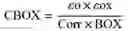
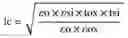
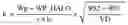
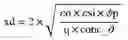
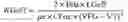
The minimum required spacing between two adjacent BTS (SPAC) is extracted from the following set of two-equations.
Vdrop = 1 2 × Ib N × 1 q × µh × conc_ ∂ × SPAC ( Wp - xpo ) · ( tsi - xd ) < 0.5 V WGeff = N × SPAC ; N ≥ 1
where N is the number of basis-structures that are being arrayed. uh is the mobility for Holes. tsi is the thickness of front-Silicon film. Wp is the lateral dimension of the P_pocket, conc_δ is the doping concentration of P_Pocket (a common practice can be to equate conc_δ to the high doping concentration of P_Halo). xpo is the lateral depletion width within P_Pocket underneath channel at Source-side, and xd is the vertical depletion depth in P_Pocket (perpendicular to the 2D layout of FIG. 2). Derivations for the xpo and xd follow the standard expressions for junction depletion and the maximum depletion width in the ideal Silicon MOS capacitor as is described in [25].
For a high current device with large Drain bias, Ib is high. To prevent FBE, either a smaller
SPAC N
is required, or a wider Wp is required; or the both conditions together. A smaller
SPAC N
implies more BTS area. In the short-channel device, the Wp has to be maintained narrow to meet the desired low threshold-voltage [16, 25, 27], and the good Subthreshold-Slope [17], consequently the optimized design tends to reduce the
SPAC N
and increases the total summative BTS area. On the other hand, in the longer channel device, the Wp can expand more into P_Body to accommodate a same bias, with less effect on threshold-voltage and Subthreshold-Slope. Consequently the optimized design can allow larger
SPAC N
and reduced BTS area; however in the long-channel devices the WGeff is naturally larger to target the same output current as of a shorter channel device, and so tends to be their total layout periphery.
As the Gate-length continues to downscale with the more advanced processes, the optimization will focus mostly on reducing the Wp, and it consequently tends to reduce the
SPAC N ;
precision corner rounding of the BTS edges become then more critical.
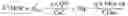
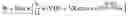
Case of a device with low drive current and low Drain bias, and depending on the channel length, the single basis-structure of FIG. 2, FIG. 3 A, FIG. 3 B and FIG. 3 C may meet the targeted electric specifications with full suppression of FBE. Expression for the Hole-component of Impact-Ionization current is [8],
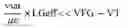
Ib = Isat × [ α Ω × ( VDS - σ × Vknee ) × exp ( - Im × Ω VDS - σ × Vknee ) ]
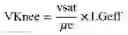
where α, σ and Ω are impact ionization constants, lm is the length of the Impact-Ionization region and Vknee is the device Knee-voltage. Saturation current drive (Isat) is function of several parameters of which are the Front-Gate bias (VFG), WGeff and the threshold-voltage. It follows the description in [26] that includes effects of short-channels and the electron Saturation-Velocity (νsat) model, and so does the Knee-voltage. The threshold-voltage in a PD SOI MOS can follow the simpler standard description used for the typical MOS capacitor [25] while accounting to effects of the Body, the P_Halo and the P_Pocket on threshold-voltage by describing its short-channel behavior similar to the descriptions in [16]. However in a FD SOI MOS of thin Silicon film, coupling does exist between the Front-Gate and the Back-Gate, and the threshold-voltage depends considerably on the Back-Gate bias (VBG). It can follow similar expressions as in [27] with the similar short-channel descriptions of [16].
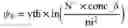
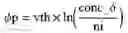
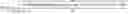
An expression for Subthreshold-Slope (SS) from [17] when the back Gate is grounded and coupling does exist between the front and the back Gates is,
SS = K . T q × VG Φ ≈ 60 × ( 1 + ( Wp ) × ɛ o × ɛ si LGeff × CFox × xd + ( ɛ si / tsi ) × CBox × ( LGeff - Wp ) LGeff × CFox × ( ( ɛ o × ɛ si / tsi ) + CBox ) )
The expression neglects the width of P_Halo at the Drain side as it is assumed small relative to the LGeff, and from the fact that it is fully depleted from the high bias to Drain; LGeff is the portion of Gate length that does not extend into N− regions. This SS expression encompasses two weighted Silicon capacitances in parallel: One capacitance for the heavily doped P_Pocket, and another capacitance for the Fully-Depleted Silicon. CFox and CBOX are the Front-Gate and the Buried Oxide capacitances per unit area. εsi is the Silicon relative dielectric constant. For a larger Wp relative to LGeff, the second ratio term inside the brackets in the above equation of SS is less significant and the SS expression approaches the known expression in PD-SOI MOS. However, for the desired design condition, and for which the Wp is intended significantly small relative to the LGeff for a lower VT and an enhanced subthreshold-slope, the first ratio term inside the brackets of same equation becomes less significant and the SS approaches the known expression for the ideal FD-SOI MOS that couples the Front-Gate to the Back-Gate entirely along its LGeff.
Design Procedure:
Design-rules specifications, such as lateral dimensions for N+ Source and N+ Drain are unrelated to our design methodology and are defined independently based on other design rules or constraints.
For given set of technology node specifications, such as the Gate dielectric thickness: tox and the LG, and for given set of process specifications such as dose of P_Halo, front Silicon film thickness (tsi), Buried Oxide Thickness (BOX), work-functions at the Front and Back Gates, etc. . . . ; the following procedure is used for optimization:
-
- A. Meeting the Electric Specifications for Threshold-Voltage (VT), Subthreshold-Slope (SS), and the Drain-Induced-Barrier-Lowering (DIBL);
- 1. Given the 4 unknowns that are: 1) carrier concentration of N−(N−), 2) Carrier concentration of P_Body (NB), 3) carrier concentration of P_Pocket (conc_δ), and 4) the lateral dimension of P_Pocket (Wp); A value for Wp is picked and the analytic expressions for the Subthreshold-Slope (SS), the threshold-voltage (VT) (after [15, 16, 27]), and the Drain-Induced-Barrier-Lowering (DIBL) are used to solve for the remaining 3 unknowns provided that target or desired values for the VT, SS and DIBL are specified. Due to the highly non-linear nature of this three-equations-system of: SS, VT, and DIBL, it can be solved with iterations.
The expression for DIBL is defined as:
Δ VT Δ VDS ,
with ΔVT being the derivative of the VT in with respect to VDS. It is function of VDS. This is because the VT itself is strong function of the VDS. Since this DIBL expression is highly non-linear with respect of VDS, the DIBL metric can be better expressed in defining two separate values for the VDS (VDS and VDSlin), and relating their magnitudes to the DIBL equation as:
DIBL = VT ( VDSlin ) - VT ( VDS ) VDSLIN - VDS
-
- This latter method is the one that we recommend and which we adopted in this work for demonstrating our design approach. This DIBL expression becomes function of the same 4 unknowns (N−, conc_δ, Wp, and NB).
- 2. WGeff is defined after [26] to meet the targeted (intended) saturation drive current for given VFG, and VT (VT depends on the Back-Gate bias VBG).
- 3. The Body current (Ib) that associates with the determined WGeff is extracted after [8].
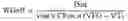
- Table 2 summarizes all the design equations that were extracted from [8, 15, 16, 26, 27] and which are usable to meet the targeted Electric Specifications in an optimized design. It further specifies the exact process parameters and the design rules that were utilized in optimizing our demonstrated design for the FD-SOI MOSFET prior to its fabrication.
The more practical approach to extract the WGeff and its corresponding bias-dependent Ib at defined threshold-voltage for the intended (targeted) drive current and supply-bias is from gauging DC electrical characteristics on similar test-structures of different peripheral widths that are free of FBE and Bipolar latch-up but dense in their overall BTS space. Such test-structures can be patterned and characterized on test-chips [28] during the product technology development cycle. Once the WGeff that meets the required drive current is determined from its corresponding test-structure on the test-chip, values of the Ib as function of the bias are then also electrically measured or extracted from this same test-structure. Transmission-Line-Model (TLM) structures [29] on same test-chips can also be utilized to extract the Hole Mobility (μh).
-
- 4. The system of two equations:
rop = 1 2 × Ib N × 1 q × µh × conc_ ∂ × SPAC ( Wp - xpo ) · ( tsi - xd ) < 0.5 V , and 1 ) WGeff = N × SPAC ; N ≥ 1 2 )
-
-
- that constitutes the main contribution to our design, is then utilized to extract the two unknowns for best area-efficiency. These two unknowns are: 1) The required number of basis-structures that need be arrayed (the N integer value), and 2) the optimal spacing (SPAC) between the two adjacent BTS. Integer N and SPAC are the only two unknowns that need be solved from the above set of two equations after all prior steps in our highlighted procedure (design methodology) get undertaken.
- 5. Round the extracted value of N to its lower integer value and adjust the SPAC correspondingly to maintain a same WGeff (N must be a single digit number such as: 1, 2, 3, etc. . . . ).
- 6. Calculate the new value for the Vdrop that will result from the changes made in the above step (step 5.), and as necessary carefully tweak or adjust the value for SPAC such that the passing criteria, that is Vdrop<0.5V, is satisfied.
- 7. Define the lateral dimensions of N− regions on both ends of the Gate. Dimension must accommodate the depletion in N−.
- The generalized block-diagram for the design flow is shown in FIG. 11.
-
While the “test-chips” approach is more effective for high-volume productions of which the anticipated future sale revenue can justify the added costs associated with the design and fabrication of the test-chips structures to gauge the required WGeff for targeted Isat and the corresponding Ib, the “equations”-based approach is more economical and may be better suited for the cost-conscious small businesses and start-ups; its drawback may be in its reduced accuracy as default magnitudes for parameters such as those of Hole Mobility, electron Saturation-Velocity, and others need to be used to model rather than to extract values for the WGeff and its corresponding II-current (or Body current Ib) at the specified bias.
DESIGN EXAMPLE
TABLE 1 displays the outputs of our design procedure for the measured DC characteristics of FIG. 9 following the “equations”-based flow that is shown in TABLE 2. A 2 μm SPAC dimension resulted in a low 0.1V peak voltage drop across the transversal dimension of P_Pocket, this is substantially below our conventionally picked 0.5V upper-limit; the voltage dropout across the P_Pocket was intentionally designed that low so to still accommodate a fully suppressed FBE and suppressed Bipolar latch-up through the possibility of applying an even higher bias to the Front-Gate (>0.8V), and for the possibility that the VDS may actually fluctuate above the 3.6V. In that particular example, a single basis-structure was sufficient to meet our intended drive current target at around the ˜3.3×10⁻⁵ A/μm, thanks to the very high doping of the P_Pocket. However this device operates best at the high VDS magnitudes due to the excessively high doping of its P_Pocket. At the higher VDS magnitudes DIBL, can be effective in allowing the device to function despite the very high doping dose of its P_Pocket. Our simulated outputs for all of the threshold-voltage, Saturation drive current, body current (II-current), DIBL and the Subthreshold-Slope were in consistent agreement with measured data on the actual device structure after fabrication. They are also TCAD simulations based on the commercial Silvaco-Atlas Physics-based simulator software (FIG. 9 and FIG. 10). Our “equation”-based flow can be further detailed to account for effect of the series resistance at Source and Drain (Rext), effect of Gate-Leakage current on Isat and the Off-state current (Ioff) as are described in [26].
| TABLE 1 |
| Process Parameters, Target Electric Specifications, and |
| the design optimization on our fabricated FD-SOI MOSFET |
| Value | |
| Process parameters | ||
| Tsi, (nm) | 35 | |
| Tox, (nm) | 9 | |
| BOX, (nm) | 500 | |
| LGeff, (nm) | 350 | |
| Target Bias | ||
| VFG (V) | 0.8 | |
| VDS (V) | 3.6 | |
| VDSlin (V) | 0.05 | |
| {grave over ( )}VBG (V) | 0 | |
| Target Electric Specification | ||
| VT, (V) | 0.71 | |
| SS (mV/Dec) | 81 | |
| DIBL | −0.0056 | |
| ISat, (A/μm) | 3.3 × 10⁻⁵ | |
| Vdrop (V) | 0.1 | |
| Optimization | ||
| Wp (nm) | 20 | |
| NB (cm−3) | 4 × 10¹⁷ | |
| Conc_δ (cm−3) | 8 × 10¹⁹ | |
| N- (cm−3) | 5 × 10¹⁹ | |
| WGeff (μm) | 2 | |
| Ib (A/μm) | 1.45 × 10⁻⁵ | |
| Integer N | 1 | |
| SPAC (A/μm) | 2 | |
| TABLE 2 |
| Design Equations and the “equation”-based design flow for optimization |
| Design Example |
| // Sec. I - CONSTANTS: |
| Electric dielectric constant in space. |
| εo = 8.85 x10⁻¹² (F/m) |
| Relative dielectric constant of Silicon. |
| εsi = 11.68 |
| relative dielectric constant of Silicon Dioxide. |
| εox = 3.9 |
| Default (or extracted) value for electron channel mobility. |
| μn = 1350 × 10−4 (m2/(V.s)) |
| Default (or extracted) value for Hole mobility. |
| μh = 480 × 10−4 (m2/(V.s)) |
| Default value for electron Saturation-Velocity. |
| vsat = 1e5; vsat = 105 (m/s) |
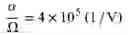
| Default values for parameters defining impact-ionization current. |
| α Ω = 4 × 10 5 ( 1 / V ) |
| lm × Ω = 50 |
| σ = 0.5 |
| Workfunction at the front Gate (Default or extracted). |
| φMSf = −0.75 (V) |
| Workfunction at the back gate (default or extracted). |
| φMSb = 0.5 (V) |
| Intrinsic carrier concentration of Silicon. |
| ni = 1.5 × 10¹⁶ (m−3) |
| Thermal-Voltage at room temperature. |
| vth = 26 × 10−3 (V) |
| Parasitic fixed charge density at the semiconductor and front Oxide interface. |
| Qff = 5 × 10⁹ (1/m2) |
| Parasitic fixed charge density at the semiconductor and BOX. |
| Qfb = 5 × 10¹⁴ (1/m2) |
| Electron charge unit. |
| q = 1.6 × 10⁻¹⁹ (C) |
| Correction factor accounting to charging in BOX. |
| Corr = 0.8 |
| // Sec. II - Technology-node specific process parameters and dimensions: |
| Physical thickness of front Silicon film. |
| tsi = 35 × 10−9 (m) |
| Physical thickness of BOX. |
| BOX = 0.5 × 10⁻⁶ (m) |
| Physical thickness of front oxide. |
| tox = 9 × 10⁻⁹ (m) |
| Effective Gate length or channel length. |
| LGeff = 0.35 × 10⁻⁶ (m) |
| Effective Gate width. |
| WGeff = 2 × 10⁻⁶ (m) |
| Constant capturing DIBL effect between technology nodes. |
| γ = 1.5 |
| // Sec. III - Targeted electric specifications. |
| Bias applied to the Front-Gate. |
| VFG = 0.8 (V) |
| Bias applied to the Back-Gate. |
| VBG = 0 (V) |
| Bias applied to Drain. |
| VDS = 3.6 (V) |
| 2nd Drain bias for DIBL calculation applicable to both, a) and b): VDSlin = 0.05 (V) |
| Dropout voltage throughout P_Pocket |
| Vdrop = 0.048 |
| Dropout voltage throughout P_Pocket |
| ISat = 3.3 × 10⁻⁵ |
| Subthreshold-Slope (SS) |
| SS = 81 × 10−3 |
| Drian-Induced-Barrier-Lowering (DIBL) |
| DIBL - −0.0056 |
| // Sec. IV - Design Equations for Calculation of threshold-voltage independent of |
| short-channel effects. |
| Case-1: The Back-Surface of Front-Silicon film that interfaces the BOX is |
| depleted: |
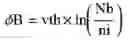
| VTHO = φ MS f - q × Qff CFox + 2 φB - q × Nb × tsi 2 × CFox + ɛo × ɛsi t si × CFox × ( 2 φB - Ψ sb ) | Eq. 1 |
| φ B = vth × ln ( Nb ni ) | |
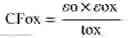
| CFox = ɛ o × ɛox tox | Eq. 2 |
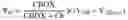
| Ψ sb = CBOX CBOX + Cb × ( V GB - V GB , acc ) | Eq. 3 |
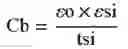
| Cb = ɛ o × ɛsi tsi | Eq. 4 |
| CBOX = ɛo × ɛox Corr × BOX | Eq. 5 |
| V GB , acc = φ MS b - Qfb CBOX - Cb CBOX × 2 × φ B - q × Nb × tsi 2 × CBOX | Eq. 6 |
| Case-2: The Back-Surface of Front-Silicon film that interfaces the BOX is |
| inverted: |
| In that case the VGB in Eq. 3 is large enough to bring the Ψsb equaling 2 × φB, |
| and the VTHO of Eq. 1 converges to: |
| VTHO = φ MS f - q × Qff CFox + 2 φB - q × Nb × tsi 2 × CFox | Eq. 7 |
| Case-3: The Back-Surface of Front-Silicon film that interfaces the BOX is |
| accumulated: |
| At the onset of accumulation the Ψsb of Eq. 1 equals 0, and the VTHO converges |
| to: |
| VTHO = φ MS f - q × Qff CFox + 2 φB - q × Nb × tsi 2 × CFox + ɛo × ɛsi tsi × CFox × 2 × φB | Eq. 8 |
| // Accounting to Short-Channel-Effects (SCE). |
| There exists a RollOff to the Threshold-Voltage due to DIBL effect, and a |
| RollUp to it as well due to effect of HALO. Both become significant at the lower |
| LGeff value. |
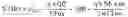
| VT = VTHO + RollOff (LGeff, VD) + RollUp(LGeff, VD) | Eq. 9 |
| RollOff ( LGeff , VD ) = - [ ( ψ 0 - 2 φB ) + VD ] × e - LGeff lc | Eq. 10 |
| ψ 0 = vth × ln ( N - × conc_δ ni 2 ) | Eq. 11 |
| lc = ɛo × ɛsi × tox × tsi ɛo × ɛox | Eq. 12 |
| RollUp ( LGeff , VD ) = [ K - 1 ] × C 2 × e - LGeff 2 × lc | Eq. 13 |
| K = Wp + WP_HALO γ × lc × ΨS2 - ΨS1 VD | Eq. 14 |
| ΨS2 = VFG − VTHO + 2 × φB | Eq. 15 |
| ΨS1 = VFG − VTHOP + 2 × φP | Eq. 16 |
| VTHOP = φ MS f - q × Qff Cof + 2 φp - q × Nb × xd CFox | Eq. 17 |
| φp = vth × ln ( conc_δ ni ) | Eq. 18 |
| xd = 2 × ɛo × ɛsi × φp q × conc_ ∂ | Eq. 19 |
| C2 = 2 × {square root over ((ψ0 − 2 × φB) × (ψ0 − 2 × φB + VD))} | Eq. 20 |
| // The Threshold-Voltage of Eq. 9 is function of only 4 unknowns that are: |
| 1. The Carrier concentration of P_Body: NB |
| 2. The Carrier concentration of P_Pocket: conc_δ |
| 3. The carrier concentration of N-region: N- |
| 4. The lateral dimension of P_Pocket: Wp |
| All other parameters are defined in Sec. I, Sec. II, & Sec. III. |
| // Sec. V - Design Equations for Calculating DIBL: |
| DIBL = VT ( VDSlin ) - VT ( VDS ) VDSlin - VDS | Eq. 21 |
| // With the VDS and the VDSlin being defined in Sec. III the DIBL of Eq. 21 is also |
| function of the same 4 unknowns as of Sec. IV and that that are: |
| 1. The Carrier concentration of P_Body: NB |
| 2. The Carrier concentration of P_Pocket: conc_δ |
| 3. The carrier concentration of N- region: N- |
| 4. The lateral dimension of P_Pocket: Wp |
| All other parameters are defined in Sec. I, Sec. II, & Sec. III. |
| // Sec. VI - Design Equations for Calculating Subthreshold-Slope (SS): |
| Expression of the SS assumes that the HALO at Drain side (P_HALO) is entirely |
| depleted at the applied VDS. Given that, the expression of SS encompasses 2 |
| weighted capacitances in parallel: One capacitance of the fully depleted |
| P_Pocket, and one capacitance of the heavily doped P_Pocket which lateral |
| width equals Wp. |
| SS ≈ 60 × ( 1 + Wp × ɛo × ɛsi LGeff × CFox × xd + ( ( ɛo × ɛsi ) / tsi ) × CBOX × ( LGeff - Wp ) LGeff × CFox ( ( ( ɛo × ɛsi ) / tsi ) + CBOX ) ) | Eq. 22 |
| // The SS of Eq. 22 is function of only 2 unknowns that are: |
| 1. The Carrier concentration of P_Pocket: conc_δ |
| 2. The lateral dimension of P_Pocket: Wp |
| All other parameters are defined in Sec. I, & Sec. II. |
| Eq. 9, Eq. 21, & Eq. 22 constitute a combined system of 3 equations with 4 unknowns. In |
| picking a value for Wp, and in knowing the target values for the VT, DIBL, and the SS, the |
| system can be solved iteratively to determine the corresponding magnitudes for: |
| 1. The Carrier concentration of P_Pocket: conc_δ |
| 2. The Carrier concentration of P_Body: NB |
| 3. The carrier concentration of N- region: N- |
| // Sec. VII - Extracting the WGeff that meets the targeted saturated drive current at |
| the targeted Front-Gate bias and VT: |
| Case-1: Drive current depends on Saturation-velocity due to the Short-Channel |
| effect defined when |
| vsat μe × LGeff << VFG - VT | Eq. 23 |
| Then the WGeff is: |
| WGeff = ISat vsat × CFox × ( VFG - VT ) | Eq. 24 |
| VKnee = vsat μe × LGeff | Eq. 25 |
| The Isat in Eq. 24 is the targeted Saturation drive current, and The VKnee of |
| Eq. 25 is the device Knee-voltage between linear and saturated drive current. |
| Case-2: Drive current depends on low-field Mobility due to the relatively long |
| LGeff. This occurs when the criteria of Eq. 23 is not met. |
| WGef f = 2 × ISat × LGeff μe × CFox × ( VFG - VT ) 2 | Eq. 26 |
| VKnee = VFG − VT | Eq. 27 |
| Given that the ISat and the VT targets are defined and so is the VFG, and rest of process |
| parameters are known, the WGeff is extracted either from Eq. 24 or from Eq. 26 depending |
| on the magnitude of the LGeff. |
| // Sec. VIII - Determining the corresponding Body-Current (Ib) for the targeted ISat |
| VFG and VDS. |
| Ib = ISat × [ u Ω × ( VDS - VKnee ) × e lm × Ω VDS - VKnee ] | Eq. 28 |
| Ib is extracted from Eq. 28. |
| // Sec. IX - Optimizing the layout. |
| SPAC ≦ 2 × Vdrop × WGeff × q × μh × conc_δ × ( Wp - xpo ) × ( tsi - xd ) Ib | Eq. 29 |
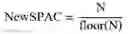
| N = WGeff SPAC | Eq. 30 |
| New SPAC = N floor ( N ) | Eq. 31 |
| NewVdrop = 1 2 × Ib floor ( N ) × 1 q × μh × conc_ ∂ × NewSPAC ( Wp - xpo ) × ( tsi - xd ) | Eq. 32 |
| xpo = 2 × ɛo × ɛsi × ψo q × [ N - conc_ ∂ × ( conc_ ∂ + N - ) ] | Eq. 33 |
| The above expression of xpo assumes that no lowering or a very minor lowering of the |
| barrier between the N- and the P_Pocket occurs due to the applied VDS. |
| The design generally targets this criterion by ensuring the high doping of P_Halo and |
| P_Pocket. As needed, the width of the P_HALO at Drain side may be widened to meet |
| this criterion. |
| N is extracted from Eq. 30 after rounding it to the lower integer, and the SPAC dimension is |
| extracted from Eq. 31. |
Claims
What is claimed is:1. The proprietary basis architecture/layout that is shown in FIG. 2, FIG. 3 A, FIG. 3 B, FIG. 3 C and FIG. 4 (FIG. 4 is for case of a SON). This claimed proprietary layout is also thoroughly described in the “DETAILED DESCRIPTION OF THE INVENTION” section.
This proprietary basis layout can be arrayed to build high-current devices following the description of our guided design methodology of that same section.
2. The design methodology that is being presented and demonstrated with this patent. It optimizes the device performance for a best area-efficient layout footprint.
Although the title of this invention is only mentioning the Silicon-On-Insulator, Silicon-On-Sapphire and Silicon-On-Nothing, the above two claims can and do cover any types of insulating and/or organic substrates.
Images & Drawings included:


Sources:
- United States Patent and Trademark Office - verify current appl. status at the USPTO↗
Similar patent applications:
Recent applications in this class:
- » 20240266441 2024-08-08
METHOD AND APPARATUS IMPROVING GATE OXIDE RELIABILITY BY CONTROLLING ACCUMULATED CHARGE - » 20240072174 2024-02-29
TRANSISTORS WITH MITIGATED FREE BODY EFFECT - » 20240072173 2024-02-29
VERTICAL SEMICONDUCTOR DEVICE WITH BODY CONTACT, METHOD OF MANUFACTURING VERTICAL SEMICONDUCTOR DEVICE WITH BODY CONTACT, AND ELECTRONIC APPARATUS - » 20220320343 2022-10-06
TRANSISTORS HAVING SELF-ALIGNED BODY TIE - » 20220181497 2022-06-09
Method and apparatus improving gate oxide reliability by controlling accumulated charge - » 20210066503 2021-03-04
Body-contacted field effect transistors configured for test and methods - » 20200335633 2020-10-22
Method and apparatus improving gate oxide reliability by controlling accumulated charge - » 20190259880 2019-08-22
Wide contact structure for small footprint radio frequency (RF) switch - » 20170358686 2017-12-14
Approach for an area-efficient and scalable CMOS performance based on advanced silicon-on-insulator (SOI), silicon-on-sapphire (SOS) and silicon-on-nothing (SON) technologies - » 20170236946 2017-08-17
Method and apparatus improving gate oxide reliability by controlling accumulated charge