Method for manufacturing an electrical circuit board, electrical circuit board obtained by this method and smart card comprising such an electrical circuit board
US20170061273A1
2017-03-02
15/242,676
2016-08-22
✅ Patent granted
US 10,102,470 B2
2018-10-16
-
-
Edwyn Labaze
Harrington & Smith
2036-08-22
Abstract:
The invention relates to a method for manufacturing an electrical circuit board. It includes the provision of a sheet of electrically conductive material and a layer of adhesive material. In order to have a colour appear in spaces cut or etched into the sheet of electrically conductive material, the adhesive material includes a colouring agent. The invention also relates to an electrical circuit board for a smart card, which circuit board is manufactured using this method, and a smart card including such an electrical circuit board.
Inventors:
- Mara COPPOLA 1 🇫🇷 Evreux, France
- Yannick DE MAQUILLE 1 🇫🇷 Paris, France
- Fabien MARCQ 1 🇫🇷 Lezoux, France
Assignee:
- Linxens Holding 36 🇫🇷 Mantes la Jolie, France
Applicant:
Interested in similar patents?
Get notified when new applications in this technology area are published.
Classification:
G06K19/07743 » CPC further
Record carriers for use with machines and with at least a part designed to carry digital markings characterised by the kind of the digital marking, e.g. shape, nature, code; Record carriers with conductive marks, printed circuits or semiconductor circuit elements, e.g. credit or identity cards also with resonating or responding marks without active components with integrated circuit chips; Constructional details, e.g. mounting of circuits in the carrier External electrical contacts
H01L23/49855 » CPC further
Details of semiconductor or other solid state devices; Arrangements for conducting electric current to or from the solid state body in operation, e.g. leads, terminal arrangements ; Selection of materials therefor consisting of soldered constructions; Leads, on insulating substrates, for flat-cards, e.g. credit cards
H05K1/0296 » CPC further
Printed circuits; Details Conductive pattern lay-out details not covered by sub groups -
H05K1/0296 » CPC further
Printed circuits; Details Conductive pattern lay-out details not covered by sub groups -
H05K1/111 » CPC further
Printed circuits; Details; Printed elements for providing electric connections to or between printed circuits Pads for surface mounting, e.g. lay-out
H05K1/111 » CPC further
Printed circuits; Details; Printed elements for providing electric connections to or between printed circuits Pads for surface mounting, e.g. lay-out
H05K1/118 » CPC further
Printed circuits; Details; Printed elements for providing electric connections to or between printed circuits specially for flexible printed circuits, e.g. using folded portions
H05K1/118 » CPC further
Printed circuits; Details; Printed elements for providing electric connections to or between printed circuits specially for flexible printed circuits, e.g. using folded portions
H05K3/10 IPC
Apparatus or processes for manufacturing printed circuits in which conductive material is applied to the insulating support in such a manner as to form the desired conductive pattern
H05K3/10 IPC
Apparatus or processes for manufacturing printed circuits in which conductive material is applied to the insulating support in such a manner as to form the desired conductive pattern
H05K3/103 » CPC further
Apparatus or processes for manufacturing printed circuits in which conductive material is applied to the insulating support in such a manner as to form the desired conductive pattern by bonding or embedding conductive wires or strips
H05K3/103 » CPC further
Apparatus or processes for manufacturing printed circuits in which conductive material is applied to the insulating support in such a manner as to form the desired conductive pattern by bonding or embedding conductive wires or strips
G06K19/077 IPC
Record carriers for use with machines and with at least a part designed to carry digital markings characterised by the kind of the digital marking, e.g. shape, nature, code; Record carriers with conductive marks, printed circuits or semiconductor circuit elements, e.g. credit or identity cards also with resonating or responding marks without active components with integrated circuit chips Constructional details, e.g. mounting of circuits in the carrier
H01L23/498 IPC
Details of semiconductor or other solid state devices; Arrangements for conducting electric current to or from the solid state body in operation, e.g. leads, terminal arrangements ; Selection of materials therefor consisting of soldered constructions Leads, on insulating substrates,
H05K1/02 IPC
Printed circuits Details
H05K1/02 IPC
Printed circuits Details
H05K1/11 IPC
Printed circuits; Details Printed elements for providing electric connections to or between printed circuits
H05K1/11 IPC
Printed circuits; Details Printed elements for providing electric connections to or between printed circuits
H05K1/18 » CPC further
Printed circuits Printed circuits structurally associated with non-printed electric components
H05K1/18 » CPC further
Printed circuits Printed circuits structurally associated with non-printed electric components
H05K3/22 » CPC further
Apparatus or processes for manufacturing printed circuits Secondary treatment of printed circuits
H05K3/22 » CPC further
Apparatus or processes for manufacturing printed circuits Secondary treatment of printed circuits
G06K19/06 IPC
Record carriers for use with machines and with at least a part designed to carry digital markings characterised by the kind of the digital marking, e.g. shape, nature, code
H05K3/07 » CPC further
Apparatus or processes for manufacturing printed circuits in which the conductive material is applied to the surface of the insulating support and is thereafter removed from such areas of the surface which are not intended for current conducting or shielding the conductive material being removed chemically or electrolytically, e.g. by photo-etch process being removed electrolytically
G06K19/07747 » CPC further
Record carriers for use with machines and with at least a part designed to carry digital markings characterised by the kind of the digital marking, e.g. shape, nature, code; Record carriers with conductive marks, printed circuits or semiconductor circuit elements, e.g. credit or identity cards also with resonating or responding marks without active components with integrated circuit chips; Constructional details, e.g. mounting of circuits in the carrier; Mounting details of integrated circuit chips at least one of the integrated circuit chips being mounted as a module
H05K2201/0112 » CPC further
Indexing scheme relating to printed circuits covered by; Dielectrics; Properties and characteristics in general Absorbing light, e.g. dielectric layer with carbon filler for laser processing
H05K2201/0112 » CPC further
Indexing scheme relating to printed circuits covered by; Dielectrics; Properties and characteristics in general Absorbing light, e.g. dielectric layer with carbon filler for laser processing
Description
The invention relates to the field of electrical circuit boards, such as printed circuit boards. Such printed circuit boards may, for example, be flexible and used to produce electronic modules for smart cards.
The invention is illustrated below using the example of electronic modules for smart cards, but it is easily transferable to other applications of rigid or flexible printed 10 circuit boards.
Smart cards are well known to the public, who makes multiple uses thereof: credit cards, travel cards, identity cards, etc.
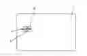
As shown in FIG. 1, smart cards are generally composed of a rigid carrier 1 made of a plastic material of PVC, PVC/ABS or polycarbonate type forming the main body of the card, with a cavity 4 into which a separately produced electronic module 2 is incorporated. This electronic module 2 comprises a generally flexible printed circuit board 3 equipped with an electronic chip 100 (integrated circuit) and transmission means for transmitting data from the chip to a card reader device (read) or from this device to the card (write). These data transmission means may be “contact” means, “contactless” means or indeed “dual” means when they combine the two preceding means. In a “contact” smart card, a connector 5 comprises contact lands 15 that are electrically connected to the chip 100 and flush with the surface of the card carrier 1, for a connection by electrical contact with a card reader device. In a “dual” smart card, in addition to the connector 5, at least one antenna is provided, generally in the card body, for a contactless connection with a card reader device.
In the prior art, the smart card modules 2 are generally formed from a dielectric substrate that is covered, on at least one of its sides 6, 7, by a sheet of electrically conductive material that is composed, for example, of a metal such as copper, steel or aluminium, or an alloy of one of these metals. Conductive tracks that form, at least in the case of some thereof, the electrical contact lands 15 are produced in this sheet of electrically conductive material. The dielectric substrates widely used in the prior art are made of composite materials (glass epoxy) or of plastic materials (PET, PEN, polyimide, etc.). This type of dielectric substrate is generally thin (its thickness is, for example, of the order of 100 μm) in order to retain a flexibility that is compatible with roll-to-roll methods for manufacturing electronic modules.
The method for manufacturing this type of electrical circuit board then comprises, for example:
-
- the provision of a sheet of electrically conductive material, which therefore has a first and a second main side;
- the provision of a layer of adhesive material;
- the placing in contact of one of the main sides of the layer of electrically conductive material with the layer of adhesive material; and
- the lamination of the sheet of electrically conductive material onto the layer of adhesive material.
A layer of dielectric material is generally used as the substrate, but the layer of adhesive material may, under certain conditions, be enough to form a dielectric substrate itself. When a layer of dielectric material is used, a step of coating one of the main sides of the layer of dielectric material with the adhesive material is carried out, in order to form the layer of adhesive material on the layer of dielectric material. The sheet of electrically conductive material is then placed in contact with the layer of adhesive material previously deposited onto the layer of dielectric material, and the assembly thus formed is subsequently laminated.
For certain applications, and in particular in the production of smart cards, it may be advantageous to obtain a visible colour in spaces cut or etched into the sheet of electrically conductive material. This colour may have a purely aesthetic function, but may also mask elements potentially positioned under the module and which would be visible between the contacts or other patterns formed in the sheet of electrically conductive material if the substrate were transparent.
To this end, the use of a dyed dielectric substrate has been proposed, but substrate suppliers, for which dyed substrates do not necessarily correspond to their standard products, are reluctant to multiply the number of their products in order to broaden the colour palette offered to their clients.
One aim of the invention is to overcome this drawback and to provide a simple means for obtaining numerous possible visible colours between at least certain areas cut or etched into the sheet of electrically conductive material.
Thus, it is proposed, according to the invention, to add a colouring agent (dye or pigment) to the adhesive material forming the layer of adhesive material, in order to form a layer of tinted or coloured adhesive material.
In this document, the following are referred to:
-
- “dye”, a material that is soluble in the medium, i.e. the adhesive material in this instance, into which it is introduced (it is said that a dye is dissolved in the medium);
- “pigment”, a material that is insoluble in the medium, i.e. the adhesive material in this instance, into which it is introduced (it is said that a pigment is dispersed in the medium).
As the layer of tinted adhesive is immediately subjacent to the sheet of electrically conductive material, its colour becomes visible between areas cut or etched into the latter, for example between conductive tracks, contacts, patterns forming logos, etc.
This method does not really modify the method of the prior art. Indeed, the layer of adhesive material is generally required. In particular, this method is much simpler than a method in which colour is added into spaces etched into the electrically conductive layer, after lamination and etching of the latter.
According to another aspect, the invention relates to an electrical circuit board comprising a sheet of electrically conductive material, with two main sides, and a layer of adhesive material in contact with one of the main sides of the layer of electrically conductive material, a colouring agent being added to the adhesive material forming the layer of adhesive material, in order to form a layer of tinted adhesive material.
According to another aspect, the invention relates to a smart card comprising a card body and a cavity made in the card body and in which an electronic module, itself comprising an electrical circuit board, is placed, with contacts that are flush with the surface of the card body and a colour that is visible on at least a portion of the surface of the module not occupied by the contacts, this colour being produced by a colouring agent present in a layer of adhesive subjacent to the contacts and added to an adhesive material in order to form a layer of tinted adhesive material.
The method, the electrical circuit board or the smart card according to the invention potentially comprises one or other of the features mentioned in the claims, considered individually or in combination.
Other features and advantages of the invention will become apparent upon reading the detailed description and the appended drawings in which:
FIG. 1 is a schematic representation in perspective of a smart card intended to receive a module comprising an electrical circuit board;
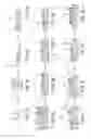
FIGS. 2a to 2l schematically represent in succession the various steps of an exemplary method for manufacturing an electrical circuit board; and
FIG. 3 is a schematic representation of an exemplary card with a module obtained via the method illustrated by FIGS. 2a to 2l.
An exemplary method for manufacturing an electrical circuit board according to the invention is described below. It belongs to the field of smart cards but, as already mentioned, what is described here may be easily transferred to applications in other fields (RFID antennas, LEDs, etc.).
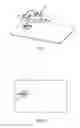
As shown in FIG. 1, a smart card 1 comprises a module 2. The module 2 comprises a flexible electrical circuit board 3, equipped with a connector 5, and a chip 100. The module 2 is generally produced in the form of a separate element which is inserted into a cavity 4 made in the card 1.
The flexible electrical circuit board 3 therefore comprises a connector 5 with multiple contact lands 15 to which the chip 100 is connected. The flexible circuit board 3 is shown (above) from its front side 6 (contact side). It is also shown (below) from its back side 7, or bonding side. The flexible electrical circuit board 3 thus shown corresponds to a single-sided flexible electrical circuit board for a “contact” card. However, it could equally be a double-sided flexible electrical circuit board, for a “dual” card for example.
FIGS. 2a to 2l schematically illustrate various steps of an exemplary method according to the invention for manufacturing the flexible electrical circuit board 3.
This method comprises the provision (FIG. 2a) of an adhesive material or glue 20, in liquid form. The adhesive material 20 is, for example, composed of (potentially modified) epoxy. At this stage, the adhesive material 20 is naturally light yellow in colour and transparent.
In the following step (FIG. 2b), the pre-formulated adhesive material 20 is coloured by the addition of a colouring agent, an actual dye or a pigment. This colouring agent may dye the adhesive material 20 e.g. red, magenta, blue, green, orange, grey, black, etc. A dyed adhesive material 30 is obtained.
Examples of dyes are given in the table below:
| Colouring agent | Chemical family | Supplier |
| Orasol ® Red 365 | Metal complex | BASF ® |
| Pylam ® Solvent Red 24 Conc | Diazo | Pylam ® |
| Pylam ® Magenta LX-7042 | Anthraquinone | Pylam ® |
| Pylam ® Blue LX-9699 | Phthalocyanine; | Pylam ® |
| anthraquinone | ||
| Pylakrome Bright Green LX-10687 | Anthraquinone; | Pylam ® |
| quinoline | ||
| Pylakrome Orange LX-10113 | Azo | Pylam ® |
The concentrations used for the dyes vary between 0.5 and 5 phr (parts per hundred resin), i.e. between 0.5 and 5 percent by weight of colouring agent with respect to the solid resin(s) (hence without the solvents) that are present in the adhesive material 20.
The colouring agent may also be a pigment. It may then be a powdered pigment (or a mixture of multiple pigments) or a pre-dispersed pigment (again with one or more pigments).
Powdered pigments are to be dispersed in a medium. Their concentration in the medium is, for example, between 0.5 and 5 phr.
Pre-dispersed pigments take the form of products containing resins and/or solvents, one or more pigments, and potential dispersing agents, additives, etc. The composition of these pre-dispersed pigments varies depending on the product itself and/or its manufacturer. Pre-dispersed pigments are easy to use as they have only to be mixed into the adhesive material. The concentration of the pigments in pre-dispersed pigments may vary widely: e.g. 10% to 70% by weight of pigment in the pre-dispersed pigment.
Chromaflo is, for example, a supplier of pre-dispersed pigments. The reference Temacolor™ EP RM15 by Chromaflo is a red pre-dispersed pigment. Used at a concentration of 20 phr, it gives good results, without negatively affecting the properties of the adhesive material. More generally, the concentration of pre-dispersed pigment in the adhesive material may be made to vary from 1 to 50 phr (or even more).
Other examples of pigments and pre-dispersed pigments are given in the table below:
| Colour | ||||
| Physical | index | |||
| Supplier | Product name | state | (C.I.) | Chemistry |
| BASF ® | Orasol ® Microlith | Powdered | Red 254 | Diketopyrrolopyrrole |
| 3630K | pigment | pre-dispersed in a vinyl | ||
| copolymer resin | ||||
| Chromaflo ™ | Temacolor ™ EP | Pre-dispersed | Red 254 | Diketopyrrolopyrrole |
| RM15 | pigment | pre-dispersed in a liquid | ||
| epoxy resin | ||||
| Temacolor ™ EP | Blue 15:3 | Copper phthalocyanine | ||
| BM15 | pre-dispersed in a liquid | |||
| epoxy resin | ||||
| Protec ® | DecoTint ® Premium | Pre-dispersed | Red 254 | Diketopyrrolopyrrole |
| I Red 644 RB | pigment | pre-dispersed in a solvent- | ||
| based PGMA resin | ||||
| DecoTint ® Premium | Blue 15:4 | Copper phthalocyanine | ||
| I Blue 675 BR | pre-dispersed in a solvent- | |||
| based PGMA resin | ||||
| Clariant(via | Hostatint Red A-P2Y | Pre-dispersed | Red 179 | Perylene pre-dispersed in a |
| Univar ®) | 100-ST | pigment | dibasic ester solvent | |
| Hostatint Blue A-BTR | Blue 15:1 | Copper phthalocyanine | ||
| 100-ST | pre-dispersed in a dibasic | |||
| ester solvent | ||||
| Trustchem | Pigment Red 254 | Powdered | Red 254 | Diketopyrrolopyrrole |
| Pigment Red 122 | pigment | Red 122 | Quinacridone | |
| Pigment Blue 60 | Blue 60 | Anthraquinone | ||
A layer of dielectric material 40, for forming a substrate 50, is provided (FIG. 2c). This dielectric material 40 is, for example, epoxy-glass. This dielectric material 40 may be grey, yellow or white in colour, for example. Its thickness is, for example, in the vicinity of 100 μm.
The layer of dielectric material 40 is next coated (FIG. 2d) with a tinted adhesive material 30 obtained in the step corresponding to FIG. 2b. The thickness of the layer of adhesive material 40 is, for example, between 10 and 70 μm after drying, and more preferably between 10 and 50 μm after drying, its thickness being, for example, 18 μm, plus or minus 3 μm.
After drying, the assembly composed of the layer of dielectric material 40 and the tinted adhesive material 30 is perforated all the way through (FIG. 2e), for example mechanically by punching, in order to form holes 42 corresponding to connection wells and, potentially, openings for receiving one or more electronic components.
A sheet of electrically conductive material 60 is placed in contact with the layer of adhesive material 30 (FIG. 2f). The sheet of electrically conductive material 60 covers the holes 42. The assembly composed of the sheet of electrically conductive material 60, of the layer of tinted adhesive material 30 and of the layer of dielectric material 40 is laminated. The layer of tinted adhesive material 30 is cured in an oven (FIG. 2g).
Resist patterns 72 are formed on the sheet of electrically conductive material 60 via photolithography, by depositing, exposing (FIG. 2h) and developing a light-sensitive resist 70 (FIG. 2i).
A step of etching patterns electrochemically allows patterns 62 to be formed in the sheet of electrically conductive material 60 (FIG. 2j). Spaces 64 between the various elements of the patterns 62 (contacts, logos) are etched into the sheet of electrically conductive material 60 and the layer of tinted adhesive material 30 is visible between these spaces 64.
The resist protecting the patterns 62 during etching is removed (FIG. 2k) and finishing layers 80 (nickel and gold for example) are potentially deposited onto the front side 6 via electrodeposition on at least a portion of the patterns 62 (FIG. 2l).
In steps that are not illustrated, a chip is fixed to the back of each module. Each chip is connected, for example via conductive wires, from the bottom of and through connection wells (like the holes 42), to contacts 15. The chip and the conductive wires are encapsulated and the modules are singulated and each one is individually transferred to a card cavity. The result is shown in FIG. 3. The colour of the tinted adhesive material 30 is visible between the contacts 15.
Numerous variants of the method described above may be envisaged. For example:
-
- the method is implemented on a double-sided circuit board, instead of the single-sided circuit board of FIG. 2l; the circuit board then comprises a sheet of conductive material on each of the two opposite sides of the layer of dielectric material; in this case, the sheet of conductive material on one of the sides may correspond to that of a copper-clad laminate with a epoxy-glass dielectric substrate, for example; and/or
- instead of etching the sheet of conductive material 60 after having laminated it onto the layer of dielectric material 40, the patterns 62 are cut into a sheet of conductive material 60, before being transferred to the layer of dielectric material 40 (lead frame technology).
Claims
1. Method for manufacturing an electrical circuit board, comprising:
the provision of a sheet of electrically conductive material, with two main sides;
the provision of a layer of adhesive material;
the placing in contact of one of the main sides of the layer of electrically conductive material with the layer of adhesive material; and
the lamination of the sheet of electrically conductive material onto the layer of adhesive material,
characterized in that a colouring agent is added to the adhesive material forming the layer of adhesive material, in order to form a layer of tinted adhesive material.
2. Method according to claim 1, comprising the provision of a layer of dielectric material having two main sides and a step of coating one of the main sides of the layer of dielectric material with the tinted adhesive material before placing one of the main sides of the electrically conductive material in contact with the layer of tinted adhesive material that is positioned on the layer of dielectric material, and laminating the sheet of electrically conductive material with the layer of dielectric material.
3. Method according to claim 1, in which the colouring agent is a dye, a powdered pigment or a pre-dispersed pigment.
4. Method according to claim 1, in which the colouring agent represents between 0.5 and 50 phr of the adhesive material.
5. Method according to claim 1, in which the colouring agent belongs to at least one of the families of chemical compounds from the list composed of metal complexes, diazos, azos, anthraquinones, diketopyrrolopyrroles, phthalocyanines, perylenes, quinacridone, and quinolines.
6. Method according to claim 1, comprising a step of producing contacts in the sheet of electrically conductive material.
7. Method according to claim 6, in which the contacts are etched into the sheet of electrically conductive material by electrochemical etching.
8. Electrical circuit board comprising a sheet of electrically conductive material, with two main sides, and a layer of adhesive material in contact with one of the main sides of the layer of electrically conductive material,
characterized in that a colouring agent is added to the adhesive material forming the layer of adhesive material, in order to form a layer of tinted adhesive material.
9. Electrical circuit board according to claim 8, additionally comprising a layer of dielectric material, the layer of tinted adhesive material being placed between the layer of dielectric material and the sheet of electrically conductive material and maintaining adhesion between the layer of dielectric material and the sheet of electrically conductive material.
10. Electrical circuit board according to claim 8, in which the colouring agent represents between 0.5 and 50 phr of the adhesive material.
11. Electrical circuit board according to claim 8, in which the colouring agent belongs to at least one of the families of chemical compounds from the list composed of metal complexes, diazos, azos, anthraquinones, diketopyrrolopyrroles, phthalocyanines, perylenes, quinacridones, and quinolines.
12. Smart card comprising a card body and a cavity made in the card body and in which an electronic module, comprising an electrical circuit board according to claim 7, is placed, the electronic module comprising contacts flush with the surface of the card body and a colour that is visible on at least a portion of the surface of the module not occupied by the contacts, this colour being produced by a colouring agent present in a layer of adhesive subjacent to the contacts and added to an adhesive material in order to form a layer of tinted adhesive material.
Images & Drawings included:
Sources:
- United States Patent and Trademark Office - verify current appl. status at the USPTO↗
Recent applications in this class:
- » 20250232151 2025-07-17
PROGRAMMABLE NETWORK NODE ROLES IN HIERARCHICAL COMMUNICATIONS NETWORK - » 20250225360 2025-07-10
RFID Tag Component, RFID Tag Assembly and Object to be Identified Attached With the RFID Tag Assembly - » 20250190740 2025-06-12
LABELED MOLDED BODY - » 20250139402 2025-05-01
RFID CONTAINER AND MANUFACTURING METHOD FOR RFID CONTAINER - » 20240419934 2024-12-19
RFID BEAD LABEL DEVICES CAPABLE OF WITHSTANDING AND MAINTAINING RFID OPERABILITY FOR IDENTIFICATION PURPOSES DURING AND POST-VULCANIZATION OF RUBBER ARTICLES - » 20240211718 2024-06-27
Programmable network node roles in hierarchical communications network - » 20240104332 2024-03-28
METHOD FOR TAGGING PRODUCTS AND A PRODUCT - » 20240070430 2024-02-29
RFID label and adherend - » 20240054313 2024-02-15
Multi-purpose RFID label - » 20230419071 2023-12-28
Smart stickers: sensors for environmental conditions
Recent applications for this Assignee:
- » 20250089175 2025-03-13
Method for Manufacturing Multicoloured Printed Circuits for Smart Card Modules - » 20240338547 2024-10-10
WIRE PAD DESIGN OF A CONNECTION PAD IN A PRELAM BODY OF A SMART CARD, PRELAM BODY, SMART CARD, METHOD OF FORMING A WIRE PAD DESIGN, AND METHOD OF FORMING A SMART CARD - » 20240220760 2024-07-04
Lead-frame, card body of a smart card, smart card, and method of forming a smart card - » 20240220758 2024-07-04
Module for integrating into a card body of a smart card, smart card, and method of implanting a module into a card body of a smart card - » 20240152721 2024-05-09
Antenna for a radio frequency identification transponder and radio frequency identification transponder - » 20240111986 2024-04-04
Card-type information substrate including a frame and a pre-form thereof - » 20240039142 2024-02-01
Method for Manufacturing Chip Card Modules and Band of Flexible Material Supporting Such Modules - » 20230376719 2023-11-23
PRELAM BODY OF A SMART CARD, SMART CARD, METHOD OF FORMING A PRELAM BODY AND METHOD OF FORMING A SMART CARD - » 20230359856 2023-11-09
Prelam body of a smart card, method of forming a prelam body of a smart card, and a smart card - » 20230274123 2023-08-31
Electrical Circuit for a Smart Card Chip Module, Smart Card Chip Module and Method for Manufacturing a Smart Card Chip Module