Copper etching integration scheme
US20170194258A1
2017-07-06
15/463,617
2017-03-20
✅ Patent granted
US 10,020,259 B2
2018-07-10
-
-
Reema Patel
Eschweiler & Potashnik, LLC
2037-03-20
Abstract:
The present disclosure relates to a method for forming an interconnect structure. In some embodiments, the method may be performed by forming an opening within a sacrificial layer. The sacrificial layer is over a substrate. A conductive material is formed within the opening and over the sacrificial layer. The conductive material within the opening defines a conductive body. The conductive material is patterned to define a conductive projection extending outward from the conductive body. The sacrificial layer is removed and a dielectric material is formed surrounding the conductive body and the conductive projection.
Inventors:
- Hsiang-Huan LEE 57 🇹🇼 Jhudong Township, Taiwan
- Chung-Ju Lee 185 🇹🇼 Hsinchu City, Taiwan
- Chih Wei Lu 121 🇹🇼 Hsinchu City, Taiwan
- Tien-I Bao 60 🇹🇼 Taoyuan City, Taiwan
- Chih Wei Lu 119 🇹🇼 Hsinchu, Taiwan
- Tien-I Bao 67 🇹🇼 Taoyuan, Taiwan
- Chung-Ju LEE 188 🇹🇼 Hsinchu, Taiwan
Assignee:
- TAIWAN SEMICONDUCTOR MANUFACTURING CO., LTD. 4,552 🇹🇼 Hsin-Chu, Taiwan
Applicant:
Interested in similar patents?
Get notified when new applications in this technology area are published.
Classification:
H01L23/5283 » CPC main
Details of semiconductor or other solid state devices; Arrangements for conducting electric current within the device in operation from one component to another, i.e. interconnections, e.g. wires, lead frames including external interconnections consisting of a multilayer structure of conductive and insulating layers inseparably formed on the semiconductor body layout of the interconnection structure Cross-sectional geometry
H01L21/7682 » CPC further
Processes or apparatus adapted for the manufacture or treatment of semiconductor or solid state devices or of parts thereof; Manufacture or treatment of devices consisting of a plurality of solid state components formed in or on a common substrate or of parts thereof; Manufacture of integrated circuit devices or of parts thereof; Manufacture of specific parts of devices defined in group; Applying interconnections to be used for carrying current between separate components within a device comprising conductors and dielectrics characterised by the formation and the after-treatment of the dielectrics, e.g. smoothing the dielectric comprising air gaps
H01L21/76885 » CPC further
Processes or apparatus adapted for the manufacture or treatment of semiconductor or solid state devices or of parts thereof; Manufacture or treatment of devices consisting of a plurality of solid state components formed in or on a common substrate or of parts thereof; Manufacture of integrated circuit devices or of parts thereof; Manufacture of specific parts of devices defined in group; Applying interconnections to be used for carrying current between separate components within a device comprising conductors and dielectrics characterised by the formation and the after-treatment of the conductors By forming conductive members before deposition of protective insulating material, e.g. pillars, studs
H01L21/76892 » CPC further
Processes or apparatus adapted for the manufacture or treatment of semiconductor or solid state devices or of parts thereof; Manufacture or treatment of devices consisting of a plurality of solid state components formed in or on a common substrate or of parts thereof; Manufacture of integrated circuit devices or of parts thereof; Manufacture of specific parts of devices defined in group; Applying interconnections to be used for carrying current between separate components within a device comprising conductors and dielectrics characterised by the formation and the after-treatment of the conductors; Modifying permanently or temporarily the pattern or the conductivity of conductive members, e.g. formation of alloys, reduction of contact resistances modifying the pattern
H01L23/5226 » CPC further
Details of semiconductor or other solid state devices; Arrangements for conducting electric current within the device in operation from one component to another, i.e. interconnections, e.g. wires, lead frames including external interconnections consisting of a multilayer structure of conductive and insulating layers inseparably formed on the semiconductor body Via connections in a multilevel interconnection structure
H01L23/5329 » CPC further
Details of semiconductor or other solid state devices; Arrangements for conducting electric current within the device in operation from one component to another, i.e. interconnections, e.g. wires, lead frames including external interconnections consisting of a multilayer structure of conductive and insulating layers inseparably formed on the semiconductor body characterised by the materials Insulating materials
H01L23/528 IPC
Details of semiconductor or other solid state devices; Arrangements for conducting electric current within the device in operation from one component to another, i.e. interconnections, e.g. wires, lead frames including external interconnections consisting of a multilayer structure of conductive and insulating layers inseparably formed on the semiconductor body layout of the interconnection structure
H01L21/3105 IPC
Processes or apparatus adapted for the manufacture or treatment of semiconductor or solid state devices or of parts thereof; Manufacture or treatment of semiconductor devices or of parts thereof the devices having at least one potential-jump barrier or surface barrier, e.g. PN junction, depletion layer or carrier concentration layer the devices having semiconductor bodies comprising elements of Group IV of the Periodic System or AB compounds with or without impurities, e.g. doping materials; Treatment of semiconductor bodies using processes or apparatus not provided for in groups - to form insulating layers thereon, e.g. for masking or by using photolithographic techniques ; After treatment of these layers; Selection of materials for these layers After-treatment
H01L21/768 IPC
Processes or apparatus adapted for the manufacture or treatment of semiconductor or solid state devices or of parts thereof; Manufacture or treatment of devices consisting of a plurality of solid state components formed in or on a common substrate or of parts thereof; Manufacture of integrated circuit devices or of parts thereof; Manufacture of specific parts of devices defined in group Applying interconnections to be used for carrying current between separate components within a device comprising conductors and dielectrics
H01L23/522 IPC
Details of semiconductor or other solid state devices; Arrangements for conducting electric current within the device in operation from one component to another, i.e. interconnections, e.g. wires, lead frames including external interconnections consisting of a multilayer structure of conductive and insulating layers inseparably formed on the semiconductor body
H01L21/00 IPC
Processes or apparatus adapted for the manufacture or treatment of semiconductor or solid state devices or of parts thereof
H01L23/532 IPC
Details of semiconductor or other solid state devices; Arrangements for conducting electric current within the device in operation from one component to another, i.e. interconnections, e.g. wires, lead frames including external interconnections consisting of a multilayer structure of conductive and insulating layers inseparably formed on the semiconductor body characterised by the materials
Description
REFERENCE TO RELATED APPLICATIONS
This Application is a Continuation of U.S. application Ser. No. 15/153,967 filed on May 13, 2016, which is a Continuation of U.S. application Ser. No. 14/218,060 filed on Mar. 18, 2014 (now U.S. Pat. No. 9,373,586 issued on Jun. 21, 2016), which is a Continuation-In-Part of U.S. application Ser. No. 13/676,260 filed on Nov. 14, 2012 (now U.S. Pat. No. 8,728,936 issued on May 20, 2014). The contents of the above-referenced applications are hereby incorporated by reference in their entirety.
BACKGROUND
As the density of semiconductor devices increases and the size of circuit elements becomes smaller, the resistance capacitance (RC) delay time increasingly dominates the circuit performance. To reduce the RC delay, there is a desire to switch from conventional dielectrics to low-k dielectrics. These materials are particularly useful as intermetal dielectrics, IMDs, and as interlayer dielectrics, ILDs. However, low-k materials present problems during processing, especially during the processing of the conductive material used to make interconnects.
BRIEF DESCRIPTION OF THE DRAWINGS
FIGS. 1A-1M are partial cross sectional views illustrating steps of one embodiment of forming an interconnect structure in accordance with the disclosure.
FIG. 2 illustrates a flow diagram of some embodiments of a method for the fabrication of an interconnect structure in accordance with the disclosure.
DETAILED DESCRIPTION
The description herein is made with reference to the drawings, wherein like reference numerals are generally utilized to refer to like elements throughout, and wherein the various structures are not necessarily drawn to scale. In the following description, for purposes of explanation, numerous specific details are set forth in order to facilitate understanding. It may be evident, however, to one of ordinary skill in the art, that one or more aspects described herein may be practiced with a lesser degree of these specific details. In other instances, known structures and devices are shown in block diagram form to facilitate understanding.
Semiconductor devices are manufactured or fabricated on semiconductor wafers using a number of different processing steps to create transistor and interconnection elements. To electrically connect transistor terminals associated with the semiconductor wafer, conductive (e.g., metal) wires, conductive vias, and the like are formed in dielectric materials as part of the semiconductor device. The conductive wires and vias couple electrical signals and power between transistors, internal circuit of the semiconductor devices, and circuits external to the semiconductor device.
In forming the interconnection elements the semiconductor wafer may undergo, for example, masking, etching, and deposition processes to form the desired electronic circuitry of the semiconductor devices. In particular, multiple masking and etching steps can be performed to form a pattern of recessed areas in a dielectric layer, such as a low-k dielectric layer, on a semiconductor wafer that serve as trenches and via holes for the interconnections. A deposition process may then be performed to deposit a metal layer over the semiconductor wafer thereby depositing metal both in the trenches and via holes and also on the non-recessed areas of the semiconductor wafer.
Increasingly, low-k dielectric layers are used to reduce signal delay and power loss effects as integrated circuit devices are scaled down. One way this has been accomplished has been to introduce porosity or dopants into the dielectric insulating layer.
As a result, the need for lower dielectric constant materials has resulted in the development of several different types of organic and inorganic low-k materials. In particular, incorporation of low-k materials with dielectric constants less than about 3.0 has become standard practice as semiconductor feature sizes have diminished to less than 0.13 microns. As feature sizes decrease below 0.13 microns, for example to 65 nm and below, materials with dielectric constants less than about 2.5 are often used. Several different organic and inorganic low-k materials have been developed and proposed for use in semiconductor devices as insulating material having dielectric constants between about 2.2 and about 3.0.
Low-k dielectric materials, however, are susceptible to damage from the etching processes because they are softer, less chemically stable or more porous, or any combination of these factors. The plasma damage can manifest itself in higher leakage currents, lower breakdown voltages, and changes in the dielectric constant associated with the low-k dielectric material.
There is, therefore, a need in the integrated circuit manufacturing art to develop a manufacturing process whereby interconnect structures may be formed without encountering the various problems presented by porous low-K dielectric layers to improve integrated circuit device yield, performance, and reliability.
Accordingly, the present disclosure is directed to methods of fabrication of an interconnect structure. The methods provide a process for defining an interconnect structure that eliminates low-k dielectric damage caused during etching processes. The process provides the further advantage of removing etch stop or NFARC (nitrogen-free anti-reflective coating) layers, making the process more cost effective.
FIGS. 1A-1M illustrate a plurality of partial cross section diagrams illustrating one embodiment of a method of forming an interconnect structure at stages in the manufacturing process according to the disclosure. Referring to FIG. 1A, a semiconductor substrate 102 having a conductive region 103 is provided. Substrate 102 is understood to include a semiconductor wafer or substrate, comprised of a semiconducting material such as silicon or germanium, or a silicon on insulator structure (SOI). Semiconductor structure can further include one or more conductive layers (such as metal or silicon) and/or insulating layers, and one or more active or passive devices formed in or over the substrate, or the like, for example, a display substrate such as a liquid crystal display (LCD), plasma display, electro-luminescence (EL) lamp display, or a light emitting diode (LED) substrate.
Overlying substrate 102 and covering conductive region 103 is a sacrificial layer 104. Sacrificial layer 104 comprises a homopolymer or copolymer. In one embodiment, sacrificial layer 104 comprises one or more of polyimide or P(neopentyl methacrylate-co-theylene glycol dimethacrylate copolymer (P(npMAco-EGDA). Sacrificial layer 104 is deposited by one or more of chemical vapor deposition (CVD) or spin-on coating processes. The thickness of the sacrificial layer will be in a range of from about 10000 Å (angstroms) to about 100 Å.
A dielectric hard mask layer 108 is then deposited 106 by, for example, a CVD process, as illustrated in FIG. 1B. The dielectric hard mask layer 108 is used to pattern the sacrificial layer 104 in a subsequent photolithographic process. In some embodiments, the dielectric hard mask layer 108 comprises a material such as silicon-oxide, silicon-nitride, silicon-oxynitride, and silicon-carbide. The dielectric hard mask layer 108 will have a thickness of from about 1000 Å to about 10 Å.
Following deposition of the hard mask layer 108, in one embodiment, a photoresist film 112 is formed by process 110 over the hard mask layer 108, as illustrated in FIG. 1C. Conventional photoresist materials may be used. The photoresist film 112 can be a carbon-containing, organic material. Various photoresists having various thicknesses can be utilized. Photo resist patterning and etching 114 are performed in FIG. 1D
Hard mask 108 patterning and first etching process 116 through the hard mask layer 108 and into the sacrificial layer 104 are then performed to remove a portion of sacrificial layer 104 and form a first feature defined by an opening 118 in the sacrificial layer 104, as shown in FIG. 1E. In one embodiment, first feature comprises a trench.
In FIG. 1F, a metal layer 124 is deposited 122 over first feature and filling opening 118 in sacrificial layer 104 to form a metal body 125 therein. Metal body 125 is defined by a lower portion 124(a) of the metal layer 124. Metal body 125 includes angled opposing sidewalls. In some embodiments, the metal body 125 comprises a metal wire layer configured to provide for a lateral interconnection (i.e., an interconnection parallel to the surface of the semiconductor substrate 102). In one embodiment, the metal layer 124 can be formed from elements such as aluminum (Al), tungsten (W), copper (Cu), copper manganese (CuMn), copper-titanium (CuTi), copper vanadium (CuV), copper chromium (CuCr), or copper-niobium (CuNb), and the like. Metal layer 124 can be formed using, for example, a plasma vapor deposition technique, among others. Metal layer 124 can be deposited at a thickness, in one embodiment, of from about 100 Å (Angstroms) to about 20,000 Å.
A photoresist film 112′ is formed over the metal layer 124 and patterned 126 by conventional techniques, as shown in FIG. 1G. A second etch 128 is performed to pattern and etch an upper portion 124(b) of the metal layer 124 to form a second feature having first recesses 123(a), 123(b) and defined by a vertical projection 127 extending from the metal body 125, as illustrated in FIG. 1H.
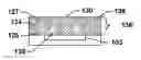
The vertical projection 127 includes angled opposing sidewalls, 129(a) and 129(b), and upper surface 130. In some embodiments, the angled opposing sidewalls, 129(a) and 129(b), are tapered such that the vertical projection 127 has a narrower top surface 127(a) and wider bottom surface 127(b) (i.e., w1<w2). In some embodiments, the vertical projection 127 comprises a metal via configured to provide for a vertical interconnection between an underlying metal body and an overlying metal body.
In FIG. 11, sacrificial layer 104 is removed by one or more of, for example, etching, wet stripping, annealing, UV or IR radiation techniques (not shown). Removal of the sacrificial layer 104 exposes angled opposing sidewalls 132(a), 132(b) of metal body 125 and forms second recesses 131(a), 131(b). Angled opposing sidewalls 132(a), 132(b) taper such that metal body 125 has a wider top surface 125(a) and narrower bottom surface 125(b).
In one embodiment, a barrier layer 134 is formed overlying and encompassing metal body 125 and vertical projection 127 and disposed between dielectric material 136 (FIG. 1K) and metal layer 124. By encompassing metal body 125 and vertical projection 127, barrier layer 134 is continuous. Barrier layer 134 is formed by depositing a dielectric material, for example, silicon-nitride and silicon-carbide. In one embodiment, barrier layer 134 is formed by depositing a metal, for example, TiN, TaN, Co, WN, TiSiN, TaSiN, or combinations thereof. In another embodiment, an annealing 135 is performed at a temperature of about greater than 200° C., such that barrier layer 134 is self-forming, as illustrated FIG. 1J. The thickness of the barrier layer 134 can be, in one embodiment, from about 1 Å (Angstrom) to about 300 Å.
In FIG. 1K, low-k dielectric material 136 is deposited by process 137 to fill first 123(a), 123(b) and second 131(a), 131(b) recesses and overlying the upper surface 130 of the vertical projection 127 to form a dielectric region 136′. Low-k dielectric material 136 thus encapsulates vertical projection 127 and metal body 125. The low-k dielectric includes dielectrics with k less than about 3. Such dielectrics include, for example, carbon-doped silicon dioxide, also referred to as organosilicate glass (OSG) and carbon-oxide. Low-k materials may also include borophosphosilicate glass (BPSG), boro silicate glass (BSG), and phosphosilicate glass (PSG), among others. The dielectric layer 136 may be formed using, for example, tetraethyl orthosilicate (TEOS), chemical vapor deposition (CVD), plasma enhanced CVD (PECVD), low pressure CVD (LPCVD), or spin-on coating techniques. The thickness of the low-k dielectric will be, in one embodiment, from about 100 Å to about 20000 Å.
In the embodiment illustrated in FIG. 1K, at least one air gap 138 is formed within the dielectric material 136. The air gap 138 is disposed in the dielectric region 136′ between angled sidewalls 132(a), 132(b) of adjacent metal bodies 125. Air gap 138 can be self-forming during deposition of the low-k material 136. In one embodiment, the size of the air gap can be from about 0 Å to about 20000 Å. It is contemplated, however, that the size of the air gap can be controlled by the low-k material 136 deposition process. A chemical mechanical polishing (CMP) process can then be performed to remove excess dielectric layer 136 and expose upper surface 130 of vertical projection 127, as illustrated in FIG. 1L.
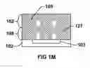
Following CMP process, the method can be repeated to form an additional metal layer 150 of an interconnect structure 152 overlying vertical projection 127 and electrically coupled to the vertical projection 127, as illustrated in FIG. 1M, so as to form an integrated circuit of at least two adjacent interconnect structures, 148 and 152.
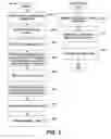
FIG. 2 illustrates a flow diagram of some embodiments of a method 200 for formation of a semiconductor structure according to an embodiment of the present disclosure. While method 200 is illustrated and described below as a series of acts or events, it will be appreciated that the illustrated ordering of such acts or events are not to be interpreted in a limiting sense. For example, some acts may occur in different orders and/or concurrently with other acts or events apart from those illustrated and/or described herein. In addition, not all illustrated acts may be required to implement one or more aspects or embodiments of the description herein. Further, one or more of the acts depicted herein may be carried out in one or more separate acts and/or phases.
At step 202 a semiconductor substrate is provided. A sacrificial layer is then formed over the substrate at step 204.
At step 206, a hard mask layer is deposited overlying the sacrificial layer.
At step 208, a first feature is formed by patterning and etching through hard mask and sacrificial layer to form an opening in the sacrificial layer.
At step 210, a metal layer is deposited overlying first feature and filling the feature opening.
At step 212, an upper portion of the metal layer is patterned and etched to form a second feature.
At step 214, sacrificial layer is removed.
At step 216, a barrier layer is formed by CVD, PVD, MOCVD or ALD, or barrier layer can be self-formed by annealing.
At step 218, a low-k dielectric material is deposited to fill recesses and encompass metal body and vertical projection.
At step 220, at least one air gap is formed in the low-k dielectric material. The air gap is disposed in the dielectric region between adjacent interconnect structures.
At step 222, a CMP process is performed to remove excess dielectric layer and expose a top surface of the vertical projection. The method then ends.
It will be appreciated that equivalent alterations and/or modifications may occur to one of ordinary skill in the art based upon a reading and/or understanding of the specification and annexed drawings. The disclosure herein includes all such modifications and alterations and is generally not intended to be limited thereby. In addition, while a particular feature or aspect may have been disclosed with respect to only one of several implementations, such feature or aspect may be combined with one or more other features and/or aspects of other implementations as may be desired. Furthermore, to the extent that the terms “includes”, “having”, “has”, “with”, and/or variants thereof are used herein, such terms are intended to be inclusive in meaning—like “comprising.” Also, “exemplary” is merely meant to mean an example, rather than the best. It is also to be appreciated that features, layers and/or elements depicted herein are illustrated with particular dimensions and/or orientations relative to one another for purposes of simplicity and ease of understanding, and that the actual dimensions and/or orientations may differ substantially from that illustrated herein.
Therefore, the disclosure relates to method for forming a conductive interconnect structure, and a related apparatus.
In some embodiments, the present disclosure relates to a method for forming an interconnect structure. The method comprises forming an opening within a sacrificial layer that is over a substrate, and forming a conductive material within the opening and over the sacrificial layer. The conductive material within the opening defines a conductive body. The method further comprises patterning the conductive material to define a conductive projection extending outward from the conductive body, and removing the sacrificial layer. The method further comprises forming a dielectric material surrounding the conductive body and the conductive projection.
In other embodiments, the present disclosure relates to a method for forming an interconnect structure. The method comprises etching one or more sacrificial materials over a substrate to define an opening extending through the one or more sacrificial materials. The method further comprises forming metal within the opening and over the one or more sacrificial materials. The metal within the opening defines a metal body. The method further comprises selectively etching the metal to define a metal projection extending from the metal body. The metal projection is set back from sidewalls of the metal body. The method further comprises removing the one or more sacrificial materials to expose opposing sidewalls of the metal body, and forming a dielectric material surrounding the metal body and the metal projection.
In yet other embodiments, the present disclosure relates to an integrated chip. The integrated chip comprises a copper body over a substrate, and a copper projection disposed on and in contact with the copper body. The copper projection has angled sidewalls that cause a width of the copper projection to decrease as a distance from the copper body increases. The copper body laterally extends past the angled sidewalls of the copper projection.
Claims
What is claimed is:1. A method for forming an interconnect structure, comprising:
forming an opening within a sacrificial layer, the sacrificial layer being over a substrate;
forming a conductive material within the opening and over the sacrificial layer, wherein the conductive material within the opening defines a conductive body;
patterning the conductive material to define a conductive projection extending outward from the conductive body;
removing the sacrificial layer; and
forming a dielectric material surrounding the conductive body and the conductive projection.
2. The method of claim 1, wherein the removing of the sacrificial layer exposes a sidewall of the conductive body.
3. The method of claim 1, wherein the sacrificial layer comprises a homopolymer or copolymer.
4. The method of claim 1, wherein the removing of the sacrificial layer exposes an upper surface of the substrate.
5. The method of claim 1, further comprising:
depositing a hard mask layer over the sacrificial layer;
patterning the hard mask layer to form a patterned hard mask layer; and
etching the sacrificial layer according to the patterned hard mask layer to form the opening in the sacrificial layer.
6. The method of claim 1, further comprising:
forming a patterned photoresist layer over the conductive material; and
etching the conductive material according to the patterned photoresist layer to define the conductive projection.
7. The method of claim 1, wherein the conductive material comprises copper and manganese.
8. The method of claim 1,
wherein the conductive projection comprises angled sidewalls that give the conductive projection a width that decreases as a distance from the conductive body increases; and
wherein the conductive body laterally extends past the angled sidewalls of the conductive projection.
9. The method of claim 1, further comprising:
concurrently forming a barrier layer over the conductive body and the conductive projection after the removing of the sacrificial layer.
10. The method of claim 9, wherein the barrier layer comprises a self-forming barrier formed by annealing the conductive body and the conductive projection at a temperature of greater than approximately 200° C.
11. The method of claim 9, wherein the barrier layer continuously extends along sidewalls and upper surfaces of the conductive body and the conductive projection.
12. A method for forming an interconnect structure, comprising:
etching one or more sacrificial materials over a substrate to define an opening extending through the one or more sacrificial materials;
forming metal within the opening and over the one or more sacrificial materials, wherein the metal within the opening defines a metal body;
selectively etching the metal to define a metal projection extending from the metal body, wherein the metal projection is set back from sidewalls of the metal body;
removing the one or more sacrificial materials to expose opposing sidewalls of the metal body; and
forming a dielectric material surrounding the metal body and the metal projection.
13. The method of claim 12, further comprising:
performing a planarization process to remove the dielectric material from directly over the metal projection and to expose a topmost surface of the metal projection.
14. The method of claim 12, wherein the metal completely covers the one or more sacrificial materials prior to the selectively etching of the metal.
15. The method of claim 12, further comprising:
removing the one or more sacrificial materials using one or more of etching, wet stripping, annealing, ultraviolet (UV) radiation, and infrared (IR) radiation.
16. The method of claim 12, wherein the metal projection comprises angled sidewalls, which cause a width of the metal projection to decrease as a distance from the metal body increases.
17. The method of claim 12, further comprising:
concurrently forming a barrier layer over the metal body and the metal projection after the removing of the one or more sacrificial materials.
18. An integrated chip, comprising:
a copper body over a substrate; and
a copper projection disposed on and in contact with the copper body and having angled sidewalls that cause a width of the copper projection to decrease as a distance from the copper body increases, and wherein the copper body laterally extends past the angled sidewalls of the copper projection.
19. The integrated chip of claim 18, further comprising:
a dielectric material surrounding the copper body and the copper projection, wherein the dielectric material comprises a dielectric constant of less than approximately 3.
20. The integrated chip of claim 19, wherein the copper body has angled sidewalls that cause a width of the copper body to decrease as a distance from the copper projection increases.
Images & Drawings included:
Sources:
- United States Patent and Trademark Office - verify current appl. status at the USPTO↗
Similar patent applications:
- » 20140131872
Copper etching integration scheme - » 20140197538
Copper etching integration scheme - » 20160254225
Copper etching integration scheme - » 20180301416
Copper etching integration scheme
Recent applications in this class:
- » 20250293160 2025-09-18
SEMICONDUCTOR DEVICE WITH NECK LAYER AND METHOD FOR FABRICATING THE SAME - » 20250293159 2025-09-18
SEMICONDUCTOR DEVICE - » 20250293158 2025-09-18
SEMICONDUCTOR DEVICE WITH NECK LAYER AND METHOD FOR FABRICATING THE SAME - » 20250293157 2025-09-18
SEMICONDUCTOR DEVICE WITH NECK LAYER AND METHOD FOR FABRICATING THE SAME - » 20250293156 2025-09-18
MERGED CONTROL LINE FORMATION FOR MEMORY WITH VERTICAL TRANSISTORS - » 20250293155 2025-09-18
BACKEND TRANSISTOR FORMATION TECHNIQUES INCLUDING SEEDED EPITAXIAL GROWTH - » 20250285972 2025-09-11
BARE-DIE SMART BRIDGE CONNECTED WITH COPPER PILLARS FOR SYSTEM-IN-PACKAGE APPARATUS - » 20250285971 2025-09-11
BARE-DIE SMART BRIDGE CONNECTED WITH COPPER PILLARS FOR SYSTEM-IN-PACKAGE APPARATUS - » 20250285970 2025-09-11
MICROELECTRONIC DEVICES AND MEMORY DEVICES - » 20250285969 2025-09-11
SEMICONDUCTOR MEMORY DEVICE AND METHOD OF FABRICATING THE SAME
Recent applications for this Assignee:
- » 20240385384 2024-11-21
1D APODIZED GRATING DEVICES AND METHODS FOR SUPPRESSING OPTICAL NOISE - » 20240371674 2024-11-07
Method for PUF generation using variations in transistor threshold voltage and subthreshold leakage current - » 20240360950 2024-10-31
APPARATUS FOR STORING AND TRANSPORTING SEMICONDUCTOR ELEMENTS, AND METHOD OF MAKING THE SAME - » 20240321781 2024-09-26
ELECTROSTATIC DISCHARGE (ESD) ARRAY WITH CIRCUIT CONTROLLED SWITCHES - » 20240203997 2024-06-20
Integrated circuit device with improved layout - » 20240202374 2024-06-20
Method and apparatus for protecting a PUF generator - » 20240190701 2024-06-13
Methods for wafer bonding - » 20240154823 2024-05-09
Method and apparatus for noise injection for PUF generator characterization - » 20240153550 2024-05-09
Memory device including memory cells and edge cells - » 20240151908 2024-05-09
Fiber-to-chip grating coupler for photonic circuits