Multi-layer cooling element
US20170265294A1
2017-09-14
15/509,601
2015-09-09
✅ Patent granted
US 10,327,323 B2
2019-06-18
WO; PCT/EP2015/070618; 20150909
WO; WO2016/038094; 20160317
Mukundbhai G Patel
Fitch, Even, Tabin & Flannery, L.L.P.
2035-09-09
Abstract:
To provide more space for additional circuit elements (coils, capacitors) and/or to allow the accommodation of additional circuit elements required for shielding the circuits, the metallization regions are arranged one over the other in at least two metallization layers. The carrier body has a surface on which sintered metallization regions are arranged in a first metallization layer, said metallization regions carrying electronic components and/or being structured such that the metallization regions form resistors or coils. The metallization regions are covered, together with the components and/or the resistors or coils, by a ceramic plate, and optionally additional metallization regions are arranged in additional metallization layers on the ceramic plate and each metallization region is covered by a ceramic plate. Sintered metallization regions are arranged in a metallization layer for the purpose of accommodating circuit elements on the uppermost ceramic plate facing away from the cooling elements.
Inventors:
- Alexander Dohn 14 🇩🇪 Memmelsdorf, Germany
- Roland Leneis 7 🇩🇪 Marktredwitz, Germany
- Roland DILSCH 5 🇩🇪 Thierstein, Germany
Assignee:
- CERAMTEC GMBH 88 🇩🇪 Plochingen, Germany
Applicant:
Interested in similar patents?
Get notified when new applications in this technology area are published.
Classification:
H05K1/0203 » CPC main
Printed circuits; Details; Thermal arrangements, e.g. for cooling, heating or preventing overheating Cooling of mounted components
H05K1/0203 » CPC main
Printed circuits; Details; Thermal arrangements, e.g. for cooling, heating or preventing overheating Cooling of mounted components
H05K1/0306 » CPC further
Printed circuits; Details; Use of materials for the substrate Inorganic insulating substrates, e.g. ceramic, glass
H05K1/0306 » CPC further
Printed circuits; Details; Use of materials for the substrate Inorganic insulating substrates, e.g. ceramic, glass
H05K1/111 » CPC further
Printed circuits; Details; Printed elements for providing electric connections to or between printed circuits Pads for surface mounting, e.g. lay-out
H05K1/111 » CPC further
Printed circuits; Details; Printed elements for providing electric connections to or between printed circuits Pads for surface mounting, e.g. lay-out
H05K1/115 » CPC further
Printed circuits; Details; Printed elements for providing electric connections to or between printed circuits Via connections; Lands around holes or via connections
H05K1/115 » CPC further
Printed circuits; Details; Printed elements for providing electric connections to or between printed circuits Via connections; Lands around holes or via connections
H05K1/165 » CPC further
Printed circuits incorporating printed electric components, e.g. printed resistor, capacitor, inductor incorporating printed inductors
H05K1/165 » CPC further
Printed circuits incorporating printed electric components, e.g. printed resistor, capacitor, inductor incorporating printed inductors
H05K1/167 » CPC further
Printed circuits incorporating printed electric components, e.g. printed resistor, capacitor, inductor incorporating printed resistors
H05K1/167 » CPC further
Printed circuits incorporating printed electric components, e.g. printed resistor, capacitor, inductor incorporating printed resistors
H05K1/181 » CPC further
Printed circuits; Printed circuits structurally associated with non-printed electric components associated with surface mounted components
H05K1/181 » CPC further
Printed circuits; Printed circuits structurally associated with non-printed electric components associated with surface mounted components
H01L23/3731 » CPC further
Details of semiconductor or other solid state devices; Arrangements for cooling, heating, ventilating or temperature compensation ; Temperature sensing arrangements; Selection of materials, or shaping, to facilitate cooling or heating, e.g. heatsinks; Cooling facilitated by selection of materials for the device or materials for thermal expansion adaptation, e.g. carbon Ceramic materials or glass
H01L23/3735 » CPC further
Details of semiconductor or other solid state devices; Arrangements for cooling, heating, ventilating or temperature compensation ; Temperature sensing arrangements; Selection of materials, or shaping, to facilitate cooling or heating, e.g. heatsinks; Cooling facilitated by selection of materials for the device or materials for thermal expansion adaptation, e.g. carbon Laminates or multilayers, e.g. direct bond copper ceramic substrates
H01L23/49822 » CPC further
Details of semiconductor or other solid state devices; Arrangements for conducting electric current to or from the solid state body in operation, e.g. leads, terminal arrangements ; Selection of materials therefor consisting of soldered constructions; Leads, on insulating substrates, Multilayer substrates
H05K3/0067 » CPC further
Apparatus or processes for manufacturing printed circuits; Laminating printed circuit boards onto other substrates, e.g. metallic substrates onto an inorganic, non-metallic substrate
H05K3/0067 » CPC further
Apparatus or processes for manufacturing printed circuits; Laminating printed circuit boards onto other substrates, e.g. metallic substrates onto an inorganic, non-metallic substrate
H01L2924/0002 » CPC further
Indexing scheme for arrangements or methods for connecting or disconnecting semiconductor or solid-state bodies as covered by; Technical content checked by a classifier Not covered by any one of groups , and
H01L23/373 IPC
Details of semiconductor or other solid state devices; Arrangements for cooling, heating, ventilating or temperature compensation ; Temperature sensing arrangements; Selection of materials, or shaping, to facilitate cooling or heating, e.g. heatsinks Cooling facilitated by selection of materials for the device or materials for thermal expansion adaptation, e.g. carbon
H01L23/498 IPC
Details of semiconductor or other solid state devices; Arrangements for conducting electric current to or from the solid state body in operation, e.g. leads, terminal arrangements ; Selection of materials therefor consisting of soldered constructions Leads, on insulating substrates,
H05K3/00 IPC
Apparatus or processes for manufacturing printed circuits
H05K3/00 IPC
Apparatus or processes for manufacturing printed circuits
H05K3/1216 » CPC further
Apparatus or processes for manufacturing printed circuits in which conductive material is applied to the insulating support in such a manner as to form the desired conductive pattern using printing techniques to apply the conductive material by screen printing or stencil printing
H05K3/4038 » CPC further
Apparatus or processes for manufacturing printed circuits; Forming printed elements for providing electric connections to or between printed circuits Through-connections; Vertical interconnect access [VIA] connections
H05K3/4038 » CPC further
Apparatus or processes for manufacturing printed circuits; Forming printed elements for providing electric connections to or between printed circuits Through-connections; Vertical interconnect access [VIA] connections
H05K3/4673 » CPC further
Apparatus or processes for manufacturing printed circuits; Manufacturing multilayer circuits by building the multilayer layer by layer, i.e. build-up multilayer circuits Application methods or materials of intermediate insulating layers not specially adapted to any one of the previous methods of adding a circuit layer
H05K3/1291 » CPC further
Apparatus or processes for manufacturing printed circuits in which conductive material is applied to the insulating support in such a manner as to form the desired conductive pattern using printing techniques to apply the conductive material; After-treatment of the printed patterns, e.g. sintering or curing methods Firing or sintering at relative high temperatures for patterns on inorganic boards, e.g. co-firing of circuits on green ceramic sheets
H05K2201/066 » CPC further
Indexing scheme relating to printed circuits covered by; Thermal details Heatsink mounted on the surface of the PCB
H05K2201/066 » CPC further
Indexing scheme relating to printed circuits covered by; Thermal details Heatsink mounted on the surface of the PCB
H05K1/02 IPC
Printed circuits Details
H05K1/02 IPC
Printed circuits Details
H05K1/03 IPC
Printed circuits; Details Use of materials for the substrate
H05K1/03 IPC
Printed circuits; Details Use of materials for the substrate
H05K1/09 » CPC further
Printed circuits; Details Use of materials for the conductive, e.g. metallic pattern
H05K1/09 » CPC further
Printed circuits; Details Use of materials for the conductive, e.g. metallic pattern
H05K1/11 IPC
Printed circuits; Details Printed elements for providing electric connections to or between printed circuits
H05K1/11 IPC
Printed circuits; Details Printed elements for providing electric connections to or between printed circuits
H05K1/16 IPC
Printed circuits incorporating printed electric components, e.g. printed resistor, capacitor, inductor
H05K1/16 IPC
Printed circuits incorporating printed electric components, e.g. printed resistor, capacitor, inductor
H05K1/18 IPC
Printed circuits Printed circuits structurally associated with non-printed electric components
H05K1/18 IPC
Printed circuits Printed circuits structurally associated with non-printed electric components
H05K3/12 IPC
Apparatus or processes for manufacturing printed circuits in which conductive material is applied to the insulating support in such a manner as to form the desired conductive pattern using printing techniques to apply the conductive material
H05K3/12 IPC
Apparatus or processes for manufacturing printed circuits in which conductive material is applied to the insulating support in such a manner as to form the desired conductive pattern using printing techniques to apply the conductive material
H05K3/40 IPC
Apparatus or processes for manufacturing printed circuits Forming printed elements for providing electric connections to or between printed circuits
H05K3/40 IPC
Apparatus or processes for manufacturing printed circuits Forming printed elements for providing electric connections to or between printed circuits
H05K3/46 IPC
Apparatus or processes for manufacturing printed circuits Manufacturing multilayer circuits
H05K3/46 IPC
Apparatus or processes for manufacturing printed circuits Manufacturing multilayer circuits
Description
The invention relates to a ceramic carrier body having cooling elements and having sintered metallization regions.
Air- or liquid-cooled ceramic carrier bodies made of Al2O3 or AlN have a patterned metallization (Cu or Cu/Ni/Au, or W/Ni/Au), wherein the circuit components can be soldered directly thereon. As the result of an increasing degree of miniaturization or increasing switching frequency in power components, it may be necessary to have additional circuit elements, such as shielding, coils, or capacitors in the immediate vicinity of the components on the surface of the carrier. The increased switching frequencies used today generate high-frequency interference which must be elaborately shielded to avoid EMC problems.
The problem addressed by the invention is therefore that of advancing the design of a ceramic carrier body with cooling elements and with sintered metallization regions in such a manner that more space is available for other circuit elements (coils, capacitors) and/or it is possible to accommodate the additional circuit elements which are necessary to shield the circuits.
According to the invention, this problem is addressed by the carrier body described in claim 1.
The ceramic carrier body according to the invention is characterized by cooling elements and sintered metallization regions which are arranged in at least two metallization layers one above the other, wherein the carrier body has a surface on which are arranged, in a first metallization layer, the sintered metallization regions, which carry electronic components and/or are structured in such a manner that they form resistors or coils, and these metallization region are covered, together with the components and/or the resistors or coils, by a ceramic plate, wherein additional metallization regions of these sintered metallization regions are optionally arranged on the ceramic plate in additional metallization layers, each covered by a ceramic plate, wherein, on the uppermost ceramic plate, facing away from the cooling element, sintered metallization regions are arranged in a metallization layer to accommodate circuit elements.
So as to make it possible to accommodate additional circuit elements (coils, capacitors), or additional circuit elements which are necessary for shielding the circuits, in the limited space, according to the invention at least one additional metallization layer is therefore incorporated between the circuit layer and the cooling layer (fins or a layer with liquid cooling medium). This covered metallization can consist of the same material as the outer circuit layer, or of a different metal, preferably with a higher melting point. A contact between the metallic elements on the outside and the inside can be made by vias (punched, laser drilled) or by structures which are drawn out to the edge of the ceramic and connected externally. This inner layer can also be structured. It improves the disturbance reaction and can accommodate electronic components. Resistors and inductors can be realized by a suitable structuring and selection of a metal. This inner layer can, together with the cover layer, form capacitors which are determined by the geometry and spacing.
The cooling elements are either fins on the carrier body or cooling channels in the interior of the carrier body.
In a preferred implementation according to the invention, the additional metallization layer(s) carries/carry electronic components, and/or is/are structured such that it/they form(s) resistors or coils. The components in this case are incorporated into the metallization in such a manner that everything can be covered with a ceramic plate. When the metallization and/or the metallization layer is/are structured in such a manner that it/they form(s) resistors or coils, then the metallization forms a layer on which a ceramic plate can be easily placed.
The carrier body preferably is made of the ceramic materials aluminum oxide Al2O3 or aluminum nitride AlN. Both materials have good thermal conductivity and are not electrically conductive. The metallization regions can be easily sintered to these materials.
The uppermost metallization layer, used to accommodate the circuit elements, is preferably made of copper, and the inner metallization layers are preferably made of tungsten.
An inventive method for the production of a carrier body according to the invention is characterized in that, to produce a metallization layer after the ceramic carrier body with the cooling elements is produced,
-
- a) sub-regions of the surface of the carrier body are coated with a tungsten/glass paste by screen printing, wherein at least at one point, the tungsten/glass paste is printed up to the outer edge of the carrier body,
- b) next, the non-coated areas are printed with an insulating paste and the tungsten/glass paste and the insulating paste are subjected to binder removal,
- c) next, a polished ceramic plate is placed on the debindered pastes,
- d) and then optionally the method steps a, b, and c are repeated, in which case the ceramic plate is printed, and
- e) finally, to create lateral metallizations by means of another screen printing step with copper paste on the lateral surface of the carrier body, the inner tungsten metallizations are connected to the uppermost copper metallization.
The individual method steps are generally known. Instead of or in addition to the lateral metallizations, vias can also be incorporated between the metallizations to create an electrical connection between the inner tungsten metallizations and the uppermost copper metallization.
EXAMPLE
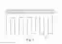
A polished cooling element 1 with fins 10 (see FIG. 1) made of AlN and having a size of 40×40×30 mm is coated 15 μm high, on the surface, with a tungsten/glass paste 2 in the form of a capacitor, by means of screen printing. By means of a complementary screen, the remaining area is printed with an insulating paste 3 (which contains a glass or the same ceramic of which the cooling element is made). The tungsten/glass paste 2 is printed at one point 4 up to the outer edge of the cooling element 1.
The tungsten-glass paste 2 and the insulating paste 3 are subjected to binder removal at 500° C. A polished ceramic plate 5 made of AlN and having dimensions of 40×40×2 mm is placed on the cooling element 1, and/or on the debindered tungsten/glass paste 2 and the insulating paste 3, and fired together with the printed cooling element 1 at 1300° C. in wet nitrogen-hydrogen. In this case, the two ceramic parts—i.e., the cooling element 1 with its fins 10 and the ceramic plate 5—connect to each other. The fired tungsten/glass paste 2 then forms an intermediate layer and/or a metallization of tungsten. The intermediate layer is also called a metallization region, and forms a metallization layer.
On the upper side of the plate 5 made of AlN, a motif or a metallization is printed with copper paste 6. The thickness of the copper paste 6 is preferably between 15 and 300 μm. The copper print and/or the copper paste 6 extends up to the outer edge 7 of the plate 5, and is connected to the tungsten intermediate layer on the lateral surface by means of a further screen printing step with copper paste 6.
The copper paste 6 and/or the copper metallization is fired in nitrogen at 910° C.
The invention therefore also describes a ceramic carrier body with cooling elements and with a circuit layer, consisting of sintered metallization regions for the purpose of accommodating circuit elements, wherein at least one additional metallization layer with sintered metallizations is arranged between the circuit layer and the carrier body, each of these additional metallizations being covered by a ceramic plate, wherein the metallizations of the circuit layer are sintered with the uppermost ceramic plate, which faces away from the cooling elements, and the sintered metallizations of the metallization layers are connected to the metallization of the circuit layer by vias, or electrically conductive structures which are drawn out to the edge of the ceramic and connected externally.
Claims
1. A ceramic carrier body, having cooling elements and having sintered metallization regions which are arranged in at least two metallization layers one above the other, wherein the carrier body has a surface on which are arranged, in a first metallization layer, sintered metallization regions which carry electronic components and/or are structured in such a manner that they form resistors or coils, and these metallization regions are covered, together with the components and/or the resistors or coils, by a ceramic plate, wherein additional metallization regions of these sintered metallization regions are optionally arranged on the ceramic plate in additional metallization layers, each covered by means of a ceramic plate, wherein, on the uppermost ceramic plate, facing away from the cooling element, sintered metallization regions are arranged in a metallization layer to accommodate circuit elements.
2. The carrier body according to claim 1, wherein the cooling elements are fins on the carrier body or cooling channels in the interior of the carrier body.
3. The carrier body according to claim 1, wherein the additional metallization layer(s) carries/carry electronic components and/or is/are structured in such a manner that it/they form(s) resistors or coils.
4. The carrier body according to claim 1, wherein the carrier body is made of the ceramic materials aluminum oxide Al2O3 or aluminum nitride AlN.
5. The carrier body according to claim 1, wherein the uppermost metallization layer for accommodating the circuit elements is made of copper, and the other inner metallization layers are made of tungsten.
6. A method for the production of a carrier body according to claim 1, wherein, to produce a metallization layer after the ceramic carrier body with the cooling elements is produced,
a) sub-regions of the surface of the carrier body are coated with a tungsten/glass paste by screen printing, wherein at least at one point, the tungsten/glass paste is printed up to the outer edge of the carrier body,
b) next, the non-coated areas are printed with an insulating paste and the tungsten/glass paste and the insulating paste are subjected to binder removal,
c) next, a polished ceramic plate is placed on the debindered pastes,
d) and then optionally the method steps a, b, and c are repeated, in which case the ceramic plate is printed, and
e) finally, to create lateral metallizations by means of another screen printing step with copper paste on the lateral surface of the carrier body, the inner tungsten metallizations are connected to the uppermost copper metallization.
7. The method according to claim 6, wherein, instead of or in addition to the lateral metallizations, vias are incorporated between the metallization layers for the purpose of electrical connection between the inner tungsten metallizations and the uppermost copper metallization.
Images & Drawings included:

Sources:
- United States Patent and Trademark Office - verify current appl. status at the USPTO↗
Recent applications in this class:
- » 20250287494 2025-09-11
ELECTRICAL CIRCUIT AND IMAGE FORMING APPARATUS - » 20250280489 2025-09-04
ELECTRONIC DEVICE FOR TRANSFERRING HEAT FROM HEATING ELEMENT TO COOLING DUCT - » 20250275053 2025-08-28
Electronic control and command assembly and groundskeeping tool provided with said electronic control and command assembly - » 20250261298 2025-08-14
ELECTRONIC DEVICE - » 20250261297 2025-08-14
ELECTRONIC DEVICE WITH A CIRCUIT ASSEMBLY - » 20250254786 2025-08-07
ELECTRONIC DEVICE - » 20250247945 2025-07-31
WORKING ASSEMBLY AND ELECTRONIC DEVICE - » 20250240866 2025-07-24
ELECTRONIC DEVICE - » 20250234451 2025-07-17
PRINTED CIRCUIT BOARD ASSEMBLY - » 20250212314 2025-06-26
DIRECT CONTACT HEAT TRANSFER COUPLINGS FOR PLUGGABLE NETWORK INTERFACE DEVICES
Recent applications for this Assignee:
- » 20210384115 2021-12-09
Module with connection lugs for supply lines - » 20210071697 2021-03-11
Connection arrangement of two components - » 20200030888 2020-01-30
Tool system - » 20190366444 2019-12-05
Tool system - » 20190091031 2019-03-28
Knee endoprosthesis for replacing at least parts of the knee joint - » 20190006578 2019-01-03
Production of lead-free piezoceramics in aqueous surroundings - » 20190001419 2019-01-03
Carrier tool, cutting insert, and clamping element - » 20170362131 2017-12-21
α/β-sialon having improved sintering activity and high edge strength - » 20170348464 2017-12-07
COMPONENTS FOR FUSING VERTEBRAL BODIES - » 20170341154 2017-11-30
Cutting insert geometry