Cable connector assembly and improved cable
US20180001407A1
2018-01-04
15/638,401
2017-06-30
✅ Patent granted
US 10,737,342 B2
2020-08-11
-
-
Amy Cohen Johnson | Paul D Baillargeon
Wei Te Chung | Ming Chieh Chang
2037-11-01
Abstract:
A cable connector assembly includes: an electrical connector; and a cable electrically connected with the electrical connector, the cable including plural high-speed wires for transmitting high-speed signal, a pair of low-speed wires for transmitting low-speed signal, a pair of power wires for transmitting power signal, a pair of standby wires, a detection wire for transmitting detection signal, and a power supply wire; wherein the pair of standby wires, the detection wire, and the power supply wire are arranged in a line along a horizontal direction; the high-speed wires are evenly distributed on both sides of the line along a thickness direction vertical to the horizontal direction; the low-speed wires are disposed on a side of the line along the thickness direction; and the power wires are disposed on another side of the line along the thickness direction.
Inventors:
- JERRY WU 381 🇺🇸 Irvine, CA, United States
- JUN CHEN 158 🇨🇳 Kunshan, China
- FAN-BO MENG 70 🇨🇳 Kunshan, China
Assignee:
- FOXCONN INTERCONNECT TECHNOLOGY LIMITED 922 Grand Cayman, Cayman Islands
Applicant:
Interested in similar patents?
Get notified when new applications in this technology area are published.
Classification:
H01R4/023 » CPC further
Electrically-conductive connections between two or more conductive members in direct contact, i.e. touching one another; Means for effecting or maintaining such contact; Electrically-conductive connections having two or more spaced connecting locations for conductors and using contact members penetrating insulation; Soldered or welded connections between cables or wires and terminals
B23K2101/38 » CPC further
Articles made by soldering, welding or cutting; Electric or electronic devices Conductors
H01B11/04 IPC
Communication cables or conductors; Cables with twisted pairs or quads with pairs or quads mutually positioned to reduce cross-talk
H01R4/02 IPC
Electrically-conductive connections between two or more conductive members in direct contact, i.e. touching one another; Means for effecting or maintaining such contact; Electrically-conductive connections having two or more spaced connecting locations for conductors and using contact members penetrating insulation Soldered or welded connections
H01R9/03 IPC
Structural associations of a plurality of mutually-insulated electrical connecting elements, e.g. terminal strips or terminal blocks; Terminals or binding posts mounted upon a base or in a case; Bases therefor Connectors arranged to contact a plurality of the conductors of a multiconductor cable, e.g. tapping connections
H01R13/6592 IPC
Details of coupling devices of the kinds covered by groups or -; Protective earth or shield arrangements on coupling devices, e.g. anti-static shielding ; High frequency shielding arrangements, e.g. against EMI [Electro-Magnetic Interference] or EMP [Electro-Magnetic Pulse]; Specific features or arrangements of connection of shield to conductive members the conductive member being a shielded cable
H01R12/59 IPC
Structural associations of a plurality of mutually-insulated electrical connecting elements, specially adapted for printed circuits, e.g. printed circuit boards [PCBs], flat or ribbon cables, or like generally planar structures, e.g. terminal strips, terminal blocks; Coupling devices specially adapted for printed circuits, flat or ribbon cables, or like generally planar structures; Terminals specially adapted for contact with, or insertion into, printed circuits, flat or ribbon cables, or like generally planar structures; Fixed connections for flexible printed circuits, flat or ribbon cables or like structures
B23K31/02 » CPC further
Processes relevant to this subclass, specially adapted for particular articles or purposes, but not covered by only one of the preceding main groups relating to soldering or welding
B23K26/22 » CPC further
Working by laser beam, e.g. welding, cutting or boring; Bonding by welding Spot welding
B23K26/32 » CPC further
Working by laser beam, e.g. welding, cutting or boring; Bonding taking account of the properties of the material involved
H01R24/60 » CPC further
Two-part coupling devices, or either of their cooperating parts, characterised by their overall structure Contacts spaced along planar side wall transverse to longitudinal axis of engagement
H01R13/6582 » CPC further
Details of coupling devices of the kinds covered by groups or -; Protective earth or shield arrangements on coupling devices, e.g. anti-static shielding ; High frequency shielding arrangements, e.g. against EMI [Electro-Magnetic Interference] or EMP [Electro-Magnetic Pulse]; Shield structure with resilient means for engaging mating connector
B23K26/24 » CPC further
Working by laser beam, e.g. welding, cutting or boring; Bonding by welding Seam welding
H01B11/1058 » CPC further
Communication cables or conductors; Cables with twisted pairs or quads with means for reducing effects of electromagnetic or electrostatic disturbances, e.g. screens; Screens specially adapted for reducing interference from external sources using a coating, e.g. a loaded polymer, ink or print
H01R12/778 » CPC further
Structural associations of a plurality of mutually-insulated electrical connecting elements, specially adapted for printed circuits, e.g. printed circuit boards [PCBs], flat or ribbon cables, or like generally planar structures, e.g. terminal strips, terminal blocks; Coupling devices specially adapted for printed circuits, flat or ribbon cables, or like generally planar structures; Terminals specially adapted for contact with, or insertion into, printed circuits, flat or ribbon cables, or like generally planar structures; Coupling devices for flexible printed circuits, flat or ribbon cables or like structures Coupling parts carrying sockets, clips or analogous counter-contacts
H01R13/6658 » CPC further
Details of coupling devices of the kinds covered by groups or -; Structural association with built-in electrical component with built-in electronic circuit on printed circuit board
H01R2107/00 » CPC further
Four or more poles
H01R13/6581 » CPC further
Details of coupling devices of the kinds covered by groups or -; Protective earth or shield arrangements on coupling devices, e.g. anti-static shielding ; High frequency shielding arrangements, e.g. against EMI [Electro-Magnetic Interference] or EMP [Electro-Magnetic Pulse] Shield structure
H01R13/665 » CPC further
Details of coupling devices of the kinds covered by groups or -; Structural association with built-in electrical component with built-in electronic circuit
B23K1/0016 » CPC main
Soldering, e.g. brazing, or unsoldering specially adapted for particular articles or work Brazing of electronic components
B23K1/00 IPC
Soldering, e.g. brazing, or unsoldering
B23K1/00 IPC
Soldering, e.g. brazing, or unsoldering
H01R12/77 IPC
Structural associations of a plurality of mutually-insulated electrical connecting elements, specially adapted for printed circuits, e.g. printed circuit boards [PCBs], flat or ribbon cables, or like generally planar structures, e.g. terminal strips, terminal blocks; Coupling devices specially adapted for printed circuits, flat or ribbon cables, or like generally planar structures; Terminals specially adapted for contact with, or insertion into, printed circuits, flat or ribbon cables, or like generally planar structures; Coupling devices for flexible printed circuits, flat or ribbon cables or like structures
H01R13/66 IPC
Details of coupling devices of the kinds covered by groups or - Structural association with built-in electrical component
H01B11/10 IPC
Communication cables or conductors; Cables with twisted pairs or quads with means for reducing effects of electromagnetic or electrostatic disturbances, e.g. screens Screens specially adapted for reducing interference from external sources
Description
BACKGROUND OF THE INVENTION
1. Field of the Invention
The present invention relates generally to a cable connector assembly and more particularly to an improved cable thereof easier to accommodate the thickness of connectors.
2. Description of Related Arts
U.S. Patent Application Publication No. 2016/0079689, published on Mar. 17, 2016, shows a cable connector assembly for high-speed signal transmission. The cable connector assembly includes a connector and a cable electrically connected to the connector. The cable includes a plurality of conductors and insulative layers enclosing the conductors. The cross section of the cable is circular such that the size thereof is large, difficult to meet the requirement of thin cable.
U.S. Pat. No. 9,620,910, issued on Apr. 11, 2017, shows a data transmission cable including a first wire and a second wire adjacent to each other. Each of the first wire and the second wire has a central conductor and a cover layer enclosing the conductor. The data transmission cable further includes grounding wires disposed between adjacent pairs of first wire and second wire.
China Patent No. 204884664, issued on Dec. 16, 2015, shows a USB Type-C flat cable including two pairs of power cords, two pairs of high-speed differential signal lines, one pair of low-speed differential signal line, one pair of control lines, a plurality of earth connection and claddings. The flat cable follows the central axis bilateral symmetry.
An improved cable wires arrangement in a cable connector assembly is desired.
SUMMARY OF THE INVENTION
An object of the present invention is to provide an improved cable in a cable connector assembly which has a reduced thickness.
To achieve the above-mentioned object, a cable connector assembly comprises: an electrical connector; and a cable electrically connected with the electrical connector, the cable including a plurality of high-speed wires for transmitting high-speed signal, a pair of low-speed wires for transmitting low-speed signal, a pair of power wires for transmitting power signal, a pair of standby wires, a detection wire for transmitting detection signal, and a power supply wire; wherein the pair of standby wires, the detection wire, and the power supply wire are arranged in a line along a horizontal direction; the high-speed wires are evenly distributed on both sides of the line along a thickness direction vertical to the horizontal direction; the low-speed wires are disposed on a side of the line along the thickness direction; and the power wires are disposed on another side of the line along the thickness direction.
BRIEF DESCRIPTION OF THE DRAWING
FIG. 1 is a perspective view of a cable connector assembly in accordance with the present invention;
FIG. 2 is an exploded view of the cable connector assembly in FIG. 1;
FIG. 3 is an exploded view similar to FIG. 2, but from a different aspect;
FIG. 4 is a partially perspective view of the assembly including the cable, the mating member and the printed circuit board;
FIG. 5 is a partially perspective view similar to the FIG. 4, but from a different aspect;
FIG. 6 is a top view of the cable and the printed circuit board of the cable connector assembly in FIG. 1;
FIG. 7 is a bottom view of the cable and the printed circuit board of the cable connector assembly in FIG. 1;
FIG. 8 is a perspective view of the cable of the cable connector assembly show in FIG. 1; and
FIG. 9 is a front view of the cable of the cable connector assembly shown in FIG. 8.
DETAILED DESCRIPTION OF THE PREFERRED EMBODIMENT
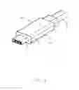
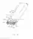
Referring to FIGS. 1 to 9, a cable connector assembly 100, in accordance with the present invention for mating with a mating connector (not shown), comprises an electrical connector 1 and a cable 2 electrically connected to the electrical connector 1. The electrical connector 1 includes a mating member 11 for being inserted to the mating connector, a printed circuit board 12 electrically connected with the mating member 11 and the cable 2, a metal case 12 enclosing the mating member 11 and the printed circuit board 12 and a outer case enclosing the metal case 13 and the cable 2.
Referring to FIGS. 2-5 and 8-9, the cable 2 includes a plurality of wires 21 and a plurality of insulative layers 22 each enclosing the corresponding wires 21. The cable is used to transmit signal conforms to USB Type C. The wires 21 includes four high-speed wires 210 for transmitting high-speed signal, a pair of low-speed wires 211 for transmitting low-speed signal, a pair of power wires 212 for transmitting power signal, a pair of standby wires 213, a detection wire 214 for transmitting detection signal, and a power supply wire 215 for the internal power supply of the electrical connector 1.
Each of the high-speed wires 210 includes a pair of coaxial wires 2100, a grounding/drain wire 2101 disposed outside the coaxial wires 2100, a shielding layer 2102 enclosing the coaxial wires 2100 and the grounding wire 2101. Each pair of coaxial wires 2100 is used to transmit a high-speed differential signal. Each of he coaxial wires 2100 includes an inner conductor 2103 and an inner insulative layer 2104 enclosing the inner conductor 2103. The low-speed wires 211 are a pair of twisted pairs for transmitting a USB 2.0 signal with a lower speed. The lower speed wires 211 may further includes a grounding wire and shielding layer, which is possible to effectively derive messy signal, and effectively reduce the external radiation and anti jamming capability of the low-speed wires 211. The pair of power wires 212 is used to transmit positive and negative signals of the power supply, respectively. The pair of standby wires 213 may be configured to transmit signals such as audio as needed.
The pair of standby wires 213, the detection wire 214, and the power supply wire 215 are arranged in a line along a horizontal/transverse direction which is vertical to a thickness/vertical direction and an extension direction. The detection wire 214 and the power supply wire 215 are disposed between the pair of standby wires 213. The four high-speed wires 210 are evenly distributed on both sides of the line along the thickness direction. The four high-speed wires 210 respectively deposed on both sides are opposite to each other along the thickness direction. The low-speed wires 211 are disposed on a side of the line along the thickness direction, and the power wires 212 are disposed on another side of the line along the thickness direction. The low-speed wires 211 are opposite to the power wires 212 along the thickness direction. The low-speed wires 211 are disposed between the pair of high-speed wires 210 located on a same side with the lower speed wires 211 along the thickness direction. The low-speed wires 211 and the power wires 212 are disposed between the power supply wire 215 and the detection wire 214 along a horizontal/transverse direction perpendicular to the thickness direction. A pair of high-speed wires 210 spaced along the thickness direction is disposed between one of the standby wires 213 and the detection wire 214, and another pair of the high-speed wires 210 spaced along the thickness direction is disposed between another standby wire 213 and the power supply wire 215. The pair of standby wires 213, the detection wire 214 and the power supply wire 215 are arranged separately from each other, by widening the spacing between each other, together with the shielding layers 2102 of the corresponding high-speed wires 210, to effectively prevent mutual coupling effect between them, thus, meets the requirements for low frequency crosstalk of the USB type C.
Referring to FIGS. 4 to 7, the printed circuit board 12 includes a top surface 120 and an opposite bottom surface 121. A rear end of the top surface 120 defines a plurality of conductive pads along the horizontal direction, which sequentially includes a pair of first high-speed conductive pads 1200 for welding with a pair of coaxial wires 2100 of a first high-speed wires 210, a first grounding conductive pad 1201 for welding with the grounding wire 2101 of the first high-speed wire 210, a first power conductive pad 1202 for welding with one of the power wires 212, a pair of low-speed conductive pads 1203 for welding with the pair of low-speed wires 211, a first standby conductive pad 1204 for welding with one of the standby wires 213, a second grounding conductive pad 1205 for welding with the grounding wire 2101 of a second high-speed wire 210, a pair of second high-speed conductive pads 1206 for welding with the pair of coaxial wires 2100 of the second high-speed wire 210. A rear end of the bottom surface 121 defines a plurality of conductive pads along the horizontal direction, which sequentially includes a pair of third high-speed conductive pads 1210 for welding with the pair of coaxial wires 2100 of a third high-speed wire 210, a third grounding conductive pad 1211 for welding with the grounding wire 2101 of the third high-speed wire 210, a detection conductive pad 1212 for welding with the detection wire 214, a power supply conductive pad 1213 for welding with the power supply wire 215, a second standby conductive pad 1214 for welding with another of the standby wires 213, a second power conductive pad 1215 for welding with another of the power wires 212, a fourth grounding conductive pad 1216 for welding with the grounding wire 2101 of a fourth high-speed wire 210 and a pair of fourth high-speed conductive pads 1217 for welding with the pair of coaxial wires 2100 of the fourth high-speed wire 210. The four high-speed wires 210 are arranged on four corner positions, most likely to avoid interference with each other. The four high-speed wires 210 correspond to the first high-speed conductive pads 1200, the second high-speed conductive pads 1206, the third high-speed conductive pads 1210 and the fourth high-speed conductive pads 1217, easy to be weld and ensure the signal integration performance of cable 2. In brief, in a cross-sectional view, there are nine positions defined by the upper level, the lower level and the middle level in the thickness direction, and a left column, the right column and the middle column in the horizontal direction wherein all the wires are respectively systematically arranged in the respective positions for easy manufacturing and superior performance.
Claims
What is claimed is:1. A cable connector assembly comprising:
an electrical connector; and
a cable electrically connected with the electrical connector, the cable including a plurality of high-speed wires for transmitting high-speed signal, a pair of low-speed wires for transmitting low-speed signal, a pair of power wires for transmitting power signal, a pair of standby wires, a detection wire for transmitting detection signal, and a power supply wire; wherein
the pair of standby wires, the detection wire, and the power supply wire are arranged in a line along a horizontal direction;
the high-speed wires are evenly distributed on both sides of the line along a thickness direction vertical to the horizontal direction;
the low-speed wires are disposed on a side of the line along the thickness direction; and
the power wires are disposed on another side of the line along the thickness direction.
2. The cable connector assembly as claimed in claim 1, wherein the low-speed wires are arranged opposite to the power wires along the thickness direction.
3. The cable connector assembly as claimed in claim 1, wherein the high-speed wires disposed on both side of the line are arranged opposite to each other along the thickness direction.
4. The cable connector assembly as claimed in claim 1, wherein the low-speed wires are disposed between the high-speed wires located on a same side of the line.
5. The cable connector assembly as claimed in claim 1, wherein the power wires are disposed between the high-speed wires located on a same side of the line.
6. The cable connector assembly as claimed in claim 1, wherein the detection wire and the power supply wire are disposed between the pair of standby wires.
7. The cable connector assembly as claimed in claim 1, wherein part of the high-speed wire are arranged between one of the standby wires and the detection wire along the horizontal direction, and the rest of the high-speed wire are arranged between another of the standby wires and the power supply wire along the horizontal direction.
8. The cable connector assembly as claimed in claim 1, wherein the low-speed wires and the power wires are arranged between the power supply wire and the detection wire along the horizontal direction.
9. The cable connector assembly as claimed in claim 1, wherein each of the high-speed wires includes a pair of coaxial wires side by side, a grounding wire arranged outside of the pair of coaxial wires and a shielding layer enclosing the coaxial wires and the grounding wire.
10. A cable comprising:
a plurality of high-speed wires for transmitting high-speed signal, a pair of low-speed wires for transmitting low-speed signal, a pair of power wires for transmitting power signal, a pair of standby wires, a detection wire for transmitting detection signal, and a power supply wire, wherein
the pair of standby wires, the detection wire, and the power supply wire are arranged in a line along a horizontal direction,
the high-speed wires are evenly distributed on both sides of the line along a thickness direction vertical to the horizontal direction,
the low-speed wires are disposed on a side of the line along the thickness direction, and
the power wires are disposed on another side of the line along the thickness direction.
11. A cable comprising:
In a cross-sectional view defined by a transverse direction and a thickness direction perpendicular to each other and defining in the thickness direction, an upper level, a lower lever and a middle level between the upper level and the lower level, and in the transverse direction, a right column, a left column and the middle column between the right column and the left column;
four pairs of high speed wires for transmitting high-speed differential signals being respectively located at four positions respectively defined by the upper level and the right column, the lower level an the right column, the upper level and the left column and the lower level;
a pair of low speed wires for transmitting low-speed differential signals being located at a position defined by the upper level and the middle column; and
a pair of power wires for delivering power being located at a position defined by the lower level and the middle column.
12. The cable as claimed in claim 11, further including a standby wire and a detection wire respectively located at two positioned defined by the middle level and intimately by two sides of the left column.
13. The cable as claimed in claim 11, further including a standby wire and a power supply wire respectively located by two positions defined by the middle level and intimately by two sides of the right column.
14. The cable as claimed in claim 13, further including another standby wire and a detection wire respectively located at two positioned defined by the middle level and intimately by two sides of the left column.
15. The cable as claimed in claim 11, where each of said four pairs of high-speed wires are equipped with a drain wire associatively.
Images & Drawings included:


Sources:
- United States Patent and Trademark Office - verify current appl. status at the USPTO↗
Similar patent applications:
- » 20140213109
Cable connector assembly having an improved cable with an equalizer function - » 20160079714
Cable connector assembly with an improved cable - » 11481151
Cable connector assembly with improved contacts - » 10873867
Cable connector assembly having improved shield members - » 12001688
Cable connector assembly with improved grounding member - » 12220307
Cable connector assembly with improved termination disposition - » 12456631
Connector assembly with improved cable retaining means - » 12221692
Cable connector assembly having improved fixing member - » 11906873
Cable connector assembly with improved wire organizer - » 11481668
Cable connector assembly with improved shell
Recent applications in this class:
- » 20250249523 2025-08-07
METHOD FOR PRODUCING ACTIVE METAL CERAMIC SUBSTRATE - » 20250222533 2025-07-10
BONDED STRUCTURE, METHOD FOR PRODUCING SAME, CONDUCTIVE MEMBER FOR SOLDER BONDING, AND STRUCTURE FOR SOLDER BONDING - » 20250222532 2025-07-10
SOLDERING WIRES OF ELECTRODES TO TIN DOMES AND PADS IN A MULTIELECTRODE CATHETER - » 20250205797 2025-06-26
METHOD OF SOLDERING ELECTRONIC DEVICES AND METHOD OF MANUFACTURING SEMICONDUCTOR PACKAGE - » 20250083243 2025-03-13
REVERSE SOLDERING CONNECTION STRUCTURE OF MICRONEEDLE AND WIRING AND PREPARATION PROCESS THEREFOR - » 20250073799 2025-03-06
IMPROVED METHOD AND ARRANGEMENT FOR A MARTENSITE-FREE BRAZING PROCESS - » 20250050439 2025-02-13
SEMICONDUCTOR PROCESSING EQUIPMENT WITH HIGH TEMPERATURE RESISTANT NICKEL ALLOY JOINTS AND METHODS FOR MAKING SAME - » 20250010390 2025-01-09
ACTIVE METAL BRAZING SUBSTRATE MATERIAL AND METHOD FOR PRODUCING THE SAME - » 20240335896 2024-10-10
Multifunctional sintering or diffusion soldering device and pressing tool - » 20240269759 2024-08-15
Circuit board assembly soldering apparatus and circuit board assembly soldering method
Recent applications for this Assignee:
- » 20240199157 2024-06-20
METHOD OF CONTROLLING STATE OF ELECTRIC ASSIST BICYCLE, CONTROL SYSTEM, AND ELECTRONIC DEVICE - » 20240177887 2024-05-30
CORE WIRE AND METHOD OF MAKING SAME AND CABLE INCLUDING THE CORE WIRE - » 20240072477 2024-02-29
ELECTRICAL CONNECTOR WITH IMPROVED CONTACTS - » 20240055792 2024-02-15
Electrical connector having an angled part and a U-shaped plate together defining a tubular structure - » 20230352880 2023-11-02
ELECTRICAL CONNECTOR WITH IMPROVED INSERTING MEMBER - » 20230335934 2023-10-19
ELECTRICAL CONNECTOR - » 20230307870 2023-09-28
Electrical connector assembly having improved locking elements - » 20230283018 2023-09-07
ELECTRICAL CONNECTOR ASSEMBLY WITH IMPROVED TERMINALS - » 20230268679 2023-08-24
Electrical connector assembly - » 20230238732 2023-07-27
ELECTRICAL CONNECTOR ASSEMBLY HAVING A METAL PLATE FOR MOUNTING A CONNECTOR TO A HOUSING