Manufacture method of AMOLED pixel drive circuit
US20180204897A1
2018-07-19
15/120,745
2016-06-27
✅ Patent granted
US 10,056,445 B2
2018-08-21
WO; PCT/CN2016/087329; 20160627
WO; WO2017/206243; 20171207
Alexander Ghyka
Leong C. Lei
2037-03-01
Abstract:
The present invention provides a manufacture method of an AMOLED pixel driving circuit. The method utilizes the oxide semiconductor thin film transistor to be the switch thin film transistor of the AMOLED pixel driving circuit to reduce the leakage current of the switch thin film transistor, and the P type polysilicon thin film transistor manufactured by utilizing the Solid Phase Crystallization is employed to be the drive thin film transistor of the AMOLED pixel driving circuit to promote the mobility, the equality and the reliability of the drive thin film transistor, and utilizing the P type thin film transistor to be the drive thin film transistor can form the constant current type OLED element, which is more stable than the source follower type OLED formed by the N type thin film transistor, and meanwhile, the parasitic capacitance is decreased with the top gate structure.
Inventors:
- Yuanjun Hsu 10 🇨🇳 Shenzhen City, China
- Yuanjun Hsu 30 🇨🇳 Shenzhen, China
- Xiaoxing ZHANG 10 🇨🇳 Shenzhen City, China
- Xingyu Zhou 9 🇨🇳 Shenzhen City, China
- Yadi Zhang 1 🇨🇳 Shenzhen City, China
- Xiaoxing ZHANG 18 🇨🇳 Shenzhen, China
- Xingyu ZHOU 26 🇨🇳 Shenzhen, China
- Yadi Zhang 1 🇨🇳 Shenzhen, China
Assignee:
- Shenzhen China Star Optoelectronics Technology Co Ltd. 3,202 🇨🇳 Shenzhen, Guangdong, China
Applicant:
Interested in similar patents?
Get notified when new applications in this technology area are published.
Classification:
H01L27/3262 » CPC main
Devices consisting of a plurality of semiconductor or other solid-state components formed in or on a common substrate including components using organic materials as the active part, or using a combination of organic materials with other materials as the active part with components specially adapted for light emission, e.g. flat-panel displays using organic light-emitting diodes [OLED]; Matrix-type displays; Active matrix displays special geometry or disposition of pixel-elements of TFT
H01L21/02043 » CPC further
Processes or apparatus adapted for the manufacture or treatment of semiconductor or solid state devices or of parts thereof; Manufacture or treatment of semiconductor devices or of parts thereof; Cleaning Cleaning before device manufacture, i.e. Begin-Of-Line process
H01L21/02565 » CPC further
Processes or apparatus adapted for the manufacture or treatment of semiconductor or solid state devices or of parts thereof; Manufacture or treatment of semiconductor devices or of parts thereof; Forming layers; Forming inorganic semiconducting materials on a substrate; Deposited layers; Materials Oxide semiconducting materials not being Group 12/16 materials, e.g. ternary compounds
H01L21/02667 » CPC further
Processes or apparatus adapted for the manufacture or treatment of semiconductor or solid state devices or of parts thereof; Manufacture or treatment of semiconductor devices or of parts thereof; Forming layers; Forming inorganic semiconducting materials on a substrate; Special treatments; Aftertreatments Crystallisation or recrystallisation of non-monocrystalline semiconductor materials, e.g. regrowth
H01L27/1218 » CPC further
Devices consisting of a plurality of semiconductor or other solid-state components formed in or on a common substrate including semiconductor components specially adapted for rectifying, oscillating, amplifying or switching and having at least one potential-jump barrier or surface barrier; including integrated passive circuit elements with at least one potential-jump barrier or surface barrier the substrate being other than a semiconductor body, e.g. an insulating body comprising a plurality of TFTs formed on a non-semiconducting substrate, e.g. driving circuits for AMLCDs with a particular composition or structure of the substrate
H01L27/1222 » CPC further
Devices consisting of a plurality of semiconductor or other solid-state components formed in or on a common substrate including semiconductor components specially adapted for rectifying, oscillating, amplifying or switching and having at least one potential-jump barrier or surface barrier; including integrated passive circuit elements with at least one potential-jump barrier or surface barrier the substrate being other than a semiconductor body, e.g. an insulating body comprising a plurality of TFTs formed on a non-semiconducting substrate, e.g. driving circuits for AMLCDs with a particular composition, shape or crystalline structure of the active layer
H01L27/1225 » CPC further
Devices consisting of a plurality of semiconductor or other solid-state components formed in or on a common substrate including semiconductor components specially adapted for rectifying, oscillating, amplifying or switching and having at least one potential-jump barrier or surface barrier; including integrated passive circuit elements with at least one potential-jump barrier or surface barrier the substrate being other than a semiconductor body, e.g. an insulating body comprising a plurality of TFTs formed on a non-semiconducting substrate, e.g. driving circuits for AMLCDs with a particular composition, shape or crystalline structure of the active layer with semiconductor materials not belonging to the group IV of the periodic table, e.g. InGaZnO
H01L27/1248 » CPC further
Devices consisting of a plurality of semiconductor or other solid-state components formed in or on a common substrate including semiconductor components specially adapted for rectifying, oscillating, amplifying or switching and having at least one potential-jump barrier or surface barrier; including integrated passive circuit elements with at least one potential-jump barrier or surface barrier the substrate being other than a semiconductor body, e.g. an insulating body comprising a plurality of TFTs formed on a non-semiconducting substrate, e.g. driving circuits for AMLCDs with a particular composition or shape of the interlayer dielectric specially adapted to the circuit arrangement
H01L27/1251 » CPC further
Devices consisting of a plurality of semiconductor or other solid-state components formed in or on a common substrate including semiconductor components specially adapted for rectifying, oscillating, amplifying or switching and having at least one potential-jump barrier or surface barrier; including integrated passive circuit elements with at least one potential-jump barrier or surface barrier the substrate being other than a semiconductor body, e.g. an insulating body comprising a plurality of TFTs formed on a non-semiconducting substrate, e.g. driving circuits for AMLCDs comprising TFTs having a different architecture, e.g. top- and bottom gate TFTs
H01L27/1255 » CPC further
Devices consisting of a plurality of semiconductor or other solid-state components formed in or on a common substrate including semiconductor components specially adapted for rectifying, oscillating, amplifying or switching and having at least one potential-jump barrier or surface barrier; including integrated passive circuit elements with at least one potential-jump barrier or surface barrier the substrate being other than a semiconductor body, e.g. an insulating body comprising a plurality of TFTs formed on a non-semiconducting substrate, e.g. driving circuits for AMLCDs integrated with passive devices, e.g. auxiliary capacitors
H01L27/1274 » CPC further
Devices consisting of a plurality of semiconductor or other solid-state components formed in or on a common substrate including semiconductor components specially adapted for rectifying, oscillating, amplifying or switching and having at least one potential-jump barrier or surface barrier; including integrated passive circuit elements with at least one potential-jump barrier or surface barrier the substrate being other than a semiconductor body, e.g. an insulating body comprising a plurality of TFTs formed on a non-semiconducting substrate, e.g. driving circuits for AMLCDs; Multistep manufacturing methods with a particular formation, treatment or patterning of the active layer specially adapted to the circuit arrangement using crystallisation of amorphous semiconductor or recrystallisation of crystalline semiconductor
H01L27/3246 » CPC further
Devices consisting of a plurality of semiconductor or other solid-state components formed in or on a common substrate including components using organic materials as the active part, or using a combination of organic materials with other materials as the active part with components specially adapted for light emission, e.g. flat-panel displays using organic light-emitting diodes [OLED]; Matrix-type displays; Active matrix displays Pixel defining structures, e.g. banks
H01L27/3248 » CPC further
Devices consisting of a plurality of semiconductor or other solid-state components formed in or on a common substrate including components using organic materials as the active part, or using a combination of organic materials with other materials as the active part with components specially adapted for light emission, e.g. flat-panel displays using organic light-emitting diodes [OLED]; Matrix-type displays; Active matrix displays Connection of the pixel electrode to the TFT
H01L29/66 IPC
Semiconductor devices adapted for rectifying, amplifying, oscillating or switching, or capacitors or resistors with at least one potential-jump barrier or surface barrier, e.g. PN junction depletion layer or carrier concentration layer; Details of semiconductor bodies or of electrodes thereof; Multistep manufacturing processes therefor Types of semiconductor device ; Multistep manufacturing processes therefor
H01L29/66969 » CPC further
Semiconductor devices adapted for rectifying, amplifying, oscillating or switching, or capacitors or resistors with at least one potential-jump barrier or surface barrier, e.g. PN junction depletion layer or carrier concentration layer; Details of semiconductor bodies or of electrodes thereof; Multistep manufacturing processes therefor; Types of semiconductor device ; Multistep manufacturing processes therefor; Multistep manufacturing processes of devices having semiconductor bodies not comprising group 14 or group 13/15 materials
H01L51/0096 » CPC further
Solid state devices using organic materials as the active part, or using a combination of organic materials with other materials as the active part; Processes or apparatus specially adapted for the manufacture or treatment of such devices, or of parts thereof Substrates
H01L51/5206 » CPC further
Solid state devices using organic materials as the active part, or using a combination of organic materials with other materials as the active part; Processes or apparatus specially adapted for the manufacture or treatment of such devices, or of parts thereof specially adapted for light emission, e.g. organic light emitting diodes [OLED] or polymer light emitting devices [PLED]; Details of devices; Electrodes Anodes, i.e. with high work-function material
H01L27/3258 » CPC further
Devices consisting of a plurality of semiconductor or other solid-state components formed in or on a common substrate including components using organic materials as the active part, or using a combination of organic materials with other materials as the active part with components specially adapted for light emission, e.g. flat-panel displays using organic light-emitting diodes [OLED]; Matrix-type displays; Active matrix displays Insulating layers formed between TFT elements and OLED elements
H01L27/3265 » CPC further
Devices consisting of a plurality of semiconductor or other solid-state components formed in or on a common substrate including components using organic materials as the active part, or using a combination of organic materials with other materials as the active part with components specially adapted for light emission, e.g. flat-panel displays using organic light-emitting diodes [OLED]; Matrix-type displays; Active matrix displays special geometry or disposition of pixel-elements of capacitor
H01L2227/323 » CPC further
Indexing scheme for devices consisting of a plurality of semiconductor or other solid state components formed in or on a common substrate covered by group; Devices including an organic light emitting device [OLED], e.g. OLED display Multistep processes for AMOLED
H01L2251/308 » CPC further
Indexing scheme relating to organic semiconductor devices covered by group; Materials; Inorganic materials; Oxides, e.g. metal oxides; Transparent conductive oxides [TCO] composed of indium oxides, e.g. ITO
H01L27/12 IPC
Devices consisting of a plurality of semiconductor or other solid-state components formed in or on a common substrate including semiconductor components specially adapted for rectifying, oscillating, amplifying or switching and having at least one potential-jump barrier or surface barrier; including integrated passive circuit elements with at least one potential-jump barrier or surface barrier the substrate being other than a semiconductor body, e.g. an insulating body
H01L27/32 IPC
Devices consisting of a plurality of semiconductor or other solid-state components formed in or on a common substrate including components using organic materials as the active part, or using a combination of organic materials with other materials as the active part with components specially adapted for light emission, e.g. flat-panel displays using organic light-emitting diodes [OLED]
H01L21/02 IPC
Processes or apparatus adapted for the manufacture or treatment of semiconductor or solid state devices or of parts thereof Manufacture or treatment of semiconductor devices or of parts thereof
H01L29/786 IPC
Semiconductor devices adapted for rectifying, amplifying, oscillating or switching, or capacitors or resistors with at least one potential-jump barrier or surface barrier, e.g. PN junction depletion layer or carrier concentration layer; Details of semiconductor bodies or of electrodes thereof; Multistep manufacturing processes therefor; Types of semiconductor device ; Multistep manufacturing processes therefor controllable by only the electric current supplied, or only the electric potential applied, to an electrode which does not carry the current to be rectified, amplified or switched; Unipolar devices, e.g. field effect transistors; Field effect transistors with field effect produced by an insulated gate Thin film transistors, i.e. transistors with a channel being at least partly a thin film
H01L29/167 » CPC further
Semiconductor devices adapted for rectifying, amplifying, oscillating or switching, or capacitors or resistors with at least one potential-jump barrier or surface barrier, e.g. PN junction depletion layer or carrier concentration layer; Details of semiconductor bodies or of electrodes thereof; Multistep manufacturing processes therefor; Semiconductor bodies ; Multistep manufacturing processes therefor characterised by the materials of which they are formed including, apart from doping materials or other impurities, only elements of Group IV of the Periodic System further characterised by the doping material
H01L51/52 IPC
Solid state devices using organic materials as the active part, or using a combination of organic materials with other materials as the active part; Processes or apparatus specially adapted for the manufacture or treatment of such devices, or of parts thereof specially adapted for light emission, e.g. organic light emitting diodes [OLED] or polymer light emitting devices [PLED] Details of devices
H01L51/00 IPC
Solid state devices using organic materials as the active part, or using a combination of organic materials with other materials as the active part; Processes or apparatus specially adapted for the manufacture or treatment of such devices, or of parts thereof
H01L29/24 » CPC further
Semiconductor devices adapted for rectifying, amplifying, oscillating or switching, or capacitors or resistors with at least one potential-jump barrier or surface barrier, e.g. PN junction depletion layer or carrier concentration layer; Details of semiconductor bodies or of electrodes thereof; Multistep manufacturing processes therefor; Semiconductor bodies ; Multistep manufacturing processes therefor characterised by the materials of which they are formed including, apart from doping materials or other impurities, only semiconductor materials not provided for in groups
H01L29/49 IPC
Semiconductor devices adapted for rectifying, amplifying, oscillating or switching, or capacitors or resistors with at least one potential-jump barrier or surface barrier, e.g. PN junction depletion layer or carrier concentration layer; Details of semiconductor bodies or of electrodes thereof; Multistep manufacturing processes therefor; Electrodes ; Multistep manufacturing processes therefor characterised by the materials of which they are formed Metal-insulator-semiconductor electrodes, e.g. gates of MOSFET
H01L21/02422 » CPC further
Processes or apparatus adapted for the manufacture or treatment of semiconductor or solid state devices or of parts thereof; Manufacture or treatment of semiconductor devices or of parts thereof; Forming layers; Forming inorganic semiconducting materials on a substrate; Substrates; Materials Non-crystalline insulating materials, e.g. glass, polymers
Description
FIELD OF THE INVENTION
The present invention relates to a display technology field, and more particularly to a manufacture method of an AMOLED pixel drive circuit.
BACKGROUND OF THE INVENTION
The Organic Light Emitting Diodes (OLED) display device possesses many outstanding properties of self-illumination, low driving voltage, high luminescence efficiency, short response time, high clarity and contrast, near 180° view angle, wide range of working temperature, applicability of flexible display and large scale full color display. The OLED is considered as the most potential display device.
The OLED can be categorized into two major types according to the driving methods, which are the Passive Matrix OLED (PMOLED) and the Active Matrix OLED (AMOLED), i.e. two types of the direct addressing and the Thin Film Transistor (TFT) matrix addressing. The AMOLED comprises pixels arranged in array and belongs to active display type, which has high lighting efficiency and is generally utilized for the large scale display devices of high resolution.
The AMOLED is a current driving element. When the electrical current flows through the organic light emitting diode, the organic light emitting diode emits light, and the brightness is determined according to the current flowing through the organic light emitting diode itself. Most of the present Integrated Circuits (IC) only transmit voltage signals. Therefore, the AMOLED pixel driving circuit needs to accomplish the task of converting the voltage signals into the current signals. The traditional AMOLED pixel driving circuit generally is 2T1C, which is a structure comprising two thin film transistors and one capacitor to convert the voltage into the current. The two thin film transistors respectively are the drive thin film transistor and the switch thin film transistor.
For the 2T1C AMOLED pixel driving circuit, the drive thin film transistor and the switch thin film transistor are usually the same type, and both are oxide thin film transistors or both are Poly Silicon thin film transistors. Although the mobility of the Low Temperature Poly Silicon (LTPS) thin film transistor based on the Excimer Laser Annealing (ELA) technology is high but the equality is poor, and the leakage current is higher. On the contrary, the equality of the oxide semiconductor thin film transistor is better, and the leakage current is low but the mobility is lower and the reliability is bad. Therefore, no matter the oxide semiconductor thin film transistor or the Poly Silicon thin film transistor is utilized, there are defects existing in the present 2T1C AMOLED pixel driving circuit.
SUMMARY OF THE INVENTION
An objective of the present invention is to provide an AMOLED pixel driving circuit, which can reduce the leakage current of the switch thin film transistor and can enhance the mobility and the reliability of the drive thin film transistor to decrease the parasitic capacitance.
For realizing the aforesaid objective, the present invention provides a manufacture method of an AMOLED pixel driving circuit, comprising steps of:
step 1, providing a substrate, and performing clean and pre-cure to the substrate;
step 2, depositing a buffer layer on the substrate, and depositing an amorphous silicon layer on the buffer layer;
step 3, performing P type ion doping and rapid thermal annealing to the amorphous silicon layer to crystallize the same into a polysilicon layer, and patterning the polysilicon layer to form a drive thin film transistor active layer and a storage capacitor lower electrode;
step 4, depositing a gate insulation layer on the drive thin film transistor active layer, the storage capacitor lower electrode and the buffer layer;
step 5, depositing a first metal layer on the gate insulation layer, and patterning the first metal layer to form a drive thin film transistor gate above the drive thin film transistor active layer and a switch thin film transistor gate, which is separately aligned with the drive thin film transistor gate, and a storage capacitor upper electrode located above the storage capacitor lower electrode;
step 6, depositing an interlayer insulation layer on the drive thin film transistor gate, the switch thin film transistor gate, the storage capacitor upper electrode and the gate insulation layer;
step 7, depositing an oxide semiconductor layer on the interlayer insulation layer, and patterning the oxide semiconductor layer to form a switch thin film transistor active layer above the switch thin film transistor gate;
step 8, patterning the interlayer insulation layer and the gate insulation layer to form a first via and a second via penetrating the interlayer insulation layer and the gate insulation layer to respectively expose two ends of the drive thin film transistor active layer with the first via and the second via;
step 9, depositing a second metal layer on the interlayer insulation layer and the switch thin film transistor active layer, and patterning the second metal layer to form a drive thin film transistor source, a drive thin film transistor drain, a switch thin film transistor source and a switch thin film transistor drain;
wherein the drive thin film transistor source and the drive thin film transistor drain respectively contact with two ends of the drive thin film transistor active layer through the first via and the second via;
the switch thin film transistor source and the switch thin film transistor drain respectively contact with two ends of the switch thin film transistor active layer;
the switch thin film transistor gate and the drive thin film transistor source are electrically coupled.
The substrate in the step 1 is a glass substrate.
All materials of the buffer layer, the gate insulation layer and the interlayer insulation layer are one or more combinations of silicon oxide and silicon nitride.
Both materials of the first metal layer and the second metal layer are molybdenum, aluminum or copper.
The P type ion doped in the step 3 is boron ion.
Material of the oxide semiconductor in the step 7 is IGZO or ITZO.
The manufacture method further comprises: step 10, sequentially forming a flat layer, a pixel electrode, a pixel definition layer and a pixel separation layer from top to bottom on the drive thin film transistor source, the drive thin film transistor drain, the switch thin film transistor source, the switch thin film transistor drain and the interlayer insulation layer.
A third via penetrating the flat layer is formed in a position on the flat layer corresponding to the drive thin film transistor drain; the pixel electrode contacts with the drive thin film transistor drain through the third via.
The pixel definition layer is formed with an opening at a position corresponding to the pixel electrode.
Material of the pixel electrode is ITO.
The present invention further provides a manufacture method of an AMOLED pixel driving circuit, comprising steps of:
step 1, providing a substrate, and performing clean and pre-cure to the substrate;
step 2, depositing a buffer layer on the substrate, and depositing an amorphous silicon layer on the buffer layer;
step 3, performing P type ion doping and rapid thermal annealing to the amorphous silicon layer to crystallize the same into a polysilicon layer, and patterning the polysilicon layer to form a drive thin film transistor active layer and a storage capacitor lower electrode;
step 4, depositing a gate insulation layer on the drive thin film transistor active layer, the storage capacitor lower electrode and the buffer layer;
step 5, depositing a first metal layer on the gate insulation layer, and patterning the first metal layer to form a drive thin film transistor gate above the drive thin film transistor active layer and a switch thin film transistor gate, which is separately aligned with the drive thin film transistor gate, and a storage capacitor upper electrode located above the storage capacitor lower electrode;
step 6, depositing an interlayer insulation layer on the drive thin film transistor gate, the switch thin film transistor gate, the storage capacitor upper electrode and the gate insulation layer;
step 7, depositing an oxide semiconductor layer on the interlayer insulation layer, and patterning the oxide semiconductor layer to form a switch thin film transistor active layer above the switch thin film transistor gate;
step 8, patterning the interlayer insulation layer and the gate insulation layer to form a first via and a second via penetrating the interlayer insulation layer and the gate insulation layer to respectively expose two ends of the drive thin film transistor active layer with the first via and the second via;
step 9, depositing a second metal layer on the interlayer insulation layer and the switch thin film transistor active layer, and patterning the second metal layer to form a drive thin film transistor source, a drive thin film transistor drain, a switch thin film transistor source and a switch thin film transistor drain;
wherein the drive thin film transistor source and the drive thin film transistor drain respectively contact with two ends of the drive thin film transistor active layer through the first via and the second via;
the switch thin film transistor source and the switch thin film transistor drain respectively contact with two ends of the switch thin film transistor active layer;
the switch thin film transistor gate and the drive thin film transistor source are electrically coupled;
wherein the substrate in the step 1 is a glass substrate;
wherein all materials of the buffer layer, the gate insulation layer and the interlayer insulation layer are one or more combinations of silicon oxide and silicon nitride;
wherein both materials of the first metal layer and the second metal layer are molybdenum, aluminum or copper.
The benefits of the present invention are: in the manufacture method of the AMOLED pixel driving circuit according to the present invention, the oxide semiconductor thin film transistor is utilized to be the switch thin film transistor of the AMOLED pixel driving circuit to reduce the leakage current of the switch thin film transistor, and the P type polysilicon thin film transistor manufactured by utilizing the Solid Phase Crystallization is employed to be the drive thin film transistor of the AMOLED pixel driving circuit to promote the mobility, the equality and the reliability of the drive thin film transistor, and utilizing the P type thin film transistor to be the drive thin film transistor can form the constant current type OLED element, which is more stable than the source follower type OLED formed by the N type thin film transistor, and meanwhile, the parasitic capacitance is decreased with the top gate structure.
BRIEF DESCRIPTION OF THE DRAWINGS
In order to better understand the characteristics and technical aspect of the invention, please refer to the following detailed description of the present invention is concerned with the diagrams, however, provide reference to the accompanying drawings and description only and is not intended to be limiting of the invention.
In drawings,
FIG. 1 is a diagram of the step 1 in the manufacture method of the AMOLED pixel driving circuit according to the present invention;
FIG. 2 is a diagram of the step 2 in the manufacture method of the AMOLED pixel driving circuit according to the present invention;
FIG. 3 is a diagram of the step 3 in the manufacture method of the AMOLED pixel driving circuit according to the present invention;
FIG. 4 is a diagram of the step 4 in the manufacture method of the AMOLED pixel driving circuit according to the present invention;
FIG. 5 is a diagram of the step 5 in the manufacture method of the AMOLED pixel driving circuit according to the present invention;
FIG. 6 is a diagram of the step 6 in the manufacture method of the AMOLED pixel driving circuit according to the present invention;
FIG. 7 is a diagram of the step 7 in the manufacture method of the AMOLED pixel driving circuit according to the present invention;
FIG. 8 is a diagram of the step 8 in the manufacture method of the AMOLED pixel driving circuit according to the present invention;
FIG. 9 is a diagram of the step 9 in the manufacture method of the AMOLED pixel driving circuit according to the present invention;
FIG. 10 is a diagram of the step 10 in the manufacture method of the AMOLED pixel driving circuit according to the present invention;
FIG. 11 is a flowchart of the manufacture method of the AMOLED pixel driving circuit according to the present invention.
DETAILED DESCRIPTION OF PREFERRED EMBODIMENTS
For better explaining the technical solution and the effect of the present invention, the present invention will be further described in detail with the accompanying drawings and the specific embodiments.
Please refer to FIG. 11. The present invention provides a manufacture method of an AMOLED pixel driving circuit, comprising steps of:
step 1, referring to FIG. 1, providing a substrate 1, and performing clean and pre-cure to the substrate 1.
Specifically, the substrate 1 is a transparent substrate and preferably to be a glass substrate.
step 2, referring to FIG. 2, depositing a buffer layer 2 on the substrate 1, and depositing an amorphous silicon layer 3′ on the buffer layer 2.
Specifically, material of the buffer layer 2 is one or more combinations of silicon oxide (SiOx) and silicon nitride (SiNx).
step 3, referring to FIG. 3, performing P type ion doping and rapid thermal annealing (RTA) to the amorphous silicon layer 3′ to crystallize the same into a polysilicon layer, and patterning the polysilicon layer to form a drive thin film transistor active layer 31 and a storage capacitor lower electrode 32.
Specifically, the P type ion doped in the step 3 is boron (B) ion. The drive thin film transistor formed in the following is a P type thin film transistor with doping the P type ions. The P type thin film transistor can manufacture the constant current type OLED element, which is more stable than the source follower type OLED formed by the N type thin film transistor.
Furthermore, utilizing the polysilicon to be the drive thin film transistor active layer can promote the equality, reliability and mobility of the drive thin film transistor.
step 4, referring to FIG. 4, depositing a gate insulation layer 4 on the drive thin film transistor active layer 31, the storage capacitor lower electrode 32 and the buffer layer 2.
Specifically, material of the gate isolation layer 4 is one or more combinations of silicon oxide and silicon nitride.
step 5, referring to FIG. 5, depositing a first metal layer on the gate insulation layer 4, and patterning the first metal layer to form a drive thin film transistor gate 41 above the drive thin film transistor active layer 31 and a switch thin film transistor gate 42, which is separately aligned with the drive thin film transistor gate 41, and a storage capacitor upper electrode 43 located above the storage capacitor lower electrode 32.
Preferably, material of the first metal layer is molybdenum (Mo), aluminum (Al) or copper (Gu). The drive thin film transistor gate 41 is above the drive thin film transistor active layer 31 and thus to form a top gate type thin film transistor. The top gate type thin film transistor can significantly decrease the parasitic capacitance of the drive thin film transistor.
The storage capacitor lower electrode 32 and the storage capacitor upper electrode 43 commonly construct the storage capacitor of the AMOLED pixel driving circuit.
step 6, referring to FIG. 6, depositing an interlayer insulation layer 5 on the drive thin film transistor gate 41, the switch thin film transistor gate 42, the storage capacitor upper electrode 43 and the gate insulation layer 4.
Specifically, material of the interlayer insulation layer 5 is one or more combinations of silicon oxide and silicon nitride.
step 7, referring to FIG. 7, depositing an oxide semiconductor layer on the interlayer insulation layer 5, and patterning the oxide semiconductor layer to form a switch thin film transistor active layer 61 above the switch thin film transistor gate 42.
Preferably, material of the oxide semiconductor layer is Indium Gallium Zinc Oxide (IGZO) or Indium Titanium Zinc Oxide (ITZO).
Furthermore, utilizing the oxide semiconductor to be the switch thin film transistor active layer 61 can reduce the leakage current of the switch thin film transistor.
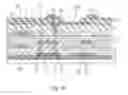
step 8, referring to FIG. 8, patterning the interlayer insulation layer 5 and the gate insulation layer 4 to form a first via 51 and a second via 52 penetrating the interlayer insulation layer 5 and the gate insulation layer 4 to respectively expose two ends of the drive thin film transistor active layer 31 with the first via 51 and the second via 52.
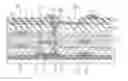
step 9, referring to FIG. 9, depositing a second metal layer on the interlayer insulation layer 5 and the switch thin film transistor active layer 61, and patterning the second metal layer to form a drive thin film transistor source 73, a drive thin film transistor drain 74, a switch thin film transistor source 71 and a switch thin film transistor drain 72.
Specifically, the drive thin film transistor source 73 and the drive thin film transistor drain 74 respectively contact with two ends of the drive thin film transistor active layer 31 through the first via 51 and the second via 52.
The drive thin film transistor source 73, the drive thin film transistor drain 74, the drive thin film transistor gate 41 and the switch thin film transistor gate 42 commonly construct the drive thin film transistor of the AMOLED pixel driving circuit.
The switch thin film transistor source 71 and the switch thin film transistor drain 72 respectively contact with two ends of the switch thin film transistor active layer 61.
The switch thin film transistor source 71, the switch thin film transistor drain 72, the switch thin film transistor gate 42 and the switch thin film transistor active layer 61 commonly construct the switch thin film transistor of the AMOLED pixel driving circuit.
The switch thin film transistor gate 72 and the drive thin film transistor source 73 are electrically coupled. The switch thin film transistor, the drive thin film transistor and the storage capacitor commonly construct a 2T1C type AMOLED pixel driving circuit.
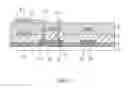
step 10, referring to FIG. 10, sequentially forming a flat layer 8, a pixel electrode 9, a pixel definition layer 10 and a pixel separation layer 11 from top to bottom on the drive thin film transistor source 73, the drive thin film transistor drain 74, the switch thin film transistor source 71, the switch thin film transistor drain 72 and the interlayer insulation layer 5.
Specifically, a third via 81 penetrating the flat layer 8 is formed in a position on the flat layer 8 corresponding to the drive thin film transistor drain 72, and the pixel electrode 9 contacts with the drive thin film transistor drain 74 through the third via 81. The pixel definition layer 10 is formed with an opening 101 at a position corresponding to the pixel electrode 9. The opening 101 is employed to deposit an organic function layer of the OLED element to form an organic light emitting diode.
Preferably, material of the flat layer 8 is one or more combinations of silicon oxide and silicon nitride.
Preferably, material of the pixel electrode 9 is Indium Tin Oxide (ITO).
In conclusion, in the manufacture method of the AMOLED pixel driving circuit according to the present invention, the oxide semiconductor thin film transistor is utilized to be the switch thin film transistor of the AMOLED pixel driving circuit to reduce the leakage current of the switch thin film transistor, and the P type polysilicon thin film transistor manufactured by utilizing the Solid Phase Crystallization is employed to be the drive thin film transistor of the AMOLED pixel driving circuit to promote the mobility, the equality and the reliability of the drive thin film transistor, and utilizing the P type thin film transistor to be the drive thin film transistor can form the constant current type OLED element, which is more stable than the source follower type OLED formed by the N type thin film transistor, and meanwhile, the parasitic capacitance is decreased with the top gate structure.
Above are only specific embodiments of the present invention, the scope of the present invention is not limited to this, and to any persons who are skilled in the art, change or replacement which is easily derived should be covered by the protected scope of the invention. Thus, the protected scope of the invention should go by the subject claims.
Claims
What is claimed is:1. A manufacture method of an AMOLED pixel driving circuit, comprising steps of:
step 1, providing a substrate, and performing clean and pre-cure to the substrate;
step 2, depositing a buffer layer on the substrate, and depositing an amorphous silicon layer on the buffer layer;
step 3, performing P type ion doping and rapid thermal annealing to the amorphous silicon layer to crystallize the same into a polysilicon layer, and patterning the polysilicon layer to form a drive thin film transistor active layer and a storage capacitor lower electrode;
step 4, depositing a gate insulation layer on the drive thin film transistor active layer, the storage capacitor lower electrode and the buffer layer;
step 5, depositing a first metal layer on the gate insulation layer, and patterning the first metal layer to form a drive thin film transistor gate above the drive thin film transistor active layer and a switch thin film transistor gate, which is separately aligned with the drive thin film transistor gate, and a storage capacitor upper electrode located above the storage capacitor lower electrode;
step 6, depositing an interlayer insulation layer on the drive thin film transistor gate, the switch thin film transistor gate, the storage capacitor upper electrode and the gate insulation layer;
step 7, depositing an oxide semiconductor layer on the interlayer insulation layer, and patterning the oxide semiconductor layer to form a switch thin film transistor active layer above the switch thin film transistor gate;
step 8, patterning the interlayer insulation layer and the gate insulation layer to form a first via and a second via penetrating the interlayer insulation layer and the gate insulation layer to respectively expose two ends of the drive thin film transistor active layer with the first via and the second via;
step 9, depositing a second metal layer on the interlayer insulation layer and the switch thin film transistor active layer, and patterning the second metal layer to form a drive thin film transistor source, a drive thin film transistor drain, a switch thin film transistor source and a switch thin film transistor drain;
wherein the drive thin film transistor source and the drive thin film transistor drain respectively contact with two ends of the drive thin film transistor active layer through the first via and the second via;
the switch thin film transistor source and the switch thin film transistor drain respectively contact with two ends of the switch thin film transistor active layer;
the switch thin film transistor gate and the drive thin film transistor source are electrically coupled.
2. The manufacture method of the AMOLED pixel driving circuit according to claim 1, wherein the substrate in the step 1 is a glass substrate.
3. The manufacture method of the AMOLED pixel driving circuit according to claim 1, wherein all materials of the buffer layer, the gate insulation layer and the interlayer insulation layer are one or more combinations of silicon oxide and silicon nitride.
4. The manufacture method of the AMOLED pixel driving circuit according to claim 1, wherein both materials of the first metal layer and the second metal layer are molybdenum, aluminum or copper.
5. The manufacture method of the AMOLED pixel driving circuit according to claim 1, wherein the P type ion doped in the step 3 is boron ion.
6. The manufacture method of the AMOLED pixel driving circuit according to claim 1, wherein material of the oxide semiconductor in the step 7 is IGZO or ITZO.
7. The manufacture method of the AMOLED pixel driving circuit according to claim 1, further comprising: step 10, sequentially forming a flat layer, a pixel electrode, a pixel definition layer and a pixel separation layer from top to bottom on the drive thin film transistor source, the drive thin film transistor drain, the switch thin film transistor source, the switch thin film transistor drain and the interlayer insulation layer.
8. The manufacture method of the AMOLED pixel driving circuit according to claim 7, wherein a third via penetrating the flat layer is formed in a position on the flat layer corresponding to the drive thin film transistor drain; the pixel electrode contacts with the drive thin film transistor drain through the third via.
9. The manufacture method of the AMOLED pixel driving circuit according to claim 7, wherein the pixel definition layer is formed with an opening at a position corresponding to the pixel electrode.
10. The manufacture method of the AMOLED pixel driving circuit according to claim 7, wherein material of the pixel electrode is ITO.
11. A manufacture method of an AMOLED pixel driving circuit, comprising steps of:
step 1, providing a substrate, and performing clean and pre-cure to the substrate;
step 2, depositing a buffer layer on the substrate, and depositing an amorphous silicon layer on the buffer layer;
step 3, performing P type ion doping and rapid thermal annealing to the amorphous silicon layer to crystallize the same into a polysilicon layer, and patterning the polysilicon layer to form a drive thin film transistor active layer and a storage capacitor lower electrode;
step 4, depositing a gate insulation layer on the drive thin film transistor active layer, the storage capacitor lower electrode and the buffer layer;
step 5, depositing a first metal layer on the gate insulation layer, and patterning the first metal layer to form a drive thin film transistor gate above the drive thin film transistor active layer and a switch thin film transistor gate, which is separately aligned with the drive thin film transistor gate, and a storage capacitor upper electrode located above the storage capacitor lower electrode;
step 6, depositing an interlayer insulation layer on the drive thin film transistor gate, the switch thin film transistor gate, the storage capacitor upper electrode and the gate insulation layer;
step 7, depositing an oxide semiconductor layer on the interlayer insulation layer, and patterning the oxide semiconductor layer to form a switch thin film transistor active layer above the switch thin film transistor gate;
step 8, patterning the interlayer insulation layer and the gate insulation layer to form a first via and a second via penetrating the interlayer insulation layer and the gate insulation layer to respectively expose two ends of the drive thin film transistor active layer with the first via and the second via;
step 9, depositing a second metal layer on the interlayer insulation layer and the switch thin film transistor active layer, and patterning the second metal layer to form a drive thin film transistor source, a drive thin film transistor drain, a switch thin film transistor source and a switch thin film transistor drain;
wherein the drive thin film transistor source and the drive thin film transistor drain respectively contact with two ends of the drive thin film transistor active layer through the first via and the second via;
the switch thin film transistor source and the switch thin film transistor drain respectively contact with two ends of the switch thin film transistor active layer;
the switch thin film transistor gate and the drive thin film transistor source are electrically coupled;
wherein the substrate in the step 1 is a glass substrate;
wherein all materials of the buffer layer, the gate insulation layer and the interlayer insulation layer are one or more combinations of silicon oxide and silicon nitride;
wherein both materials of the first metal layer and the second metal layer are molybdenum, aluminum or copper.
12. The manufacture method of the AMOLED pixel driving circuit according to claim 11, wherein the P type ion doped in the step 3 is boron ion.
13. The manufacture method of the AMOLED pixel driving circuit according to claim 11, wherein material of the oxide semiconductor in the step 7 is IGZO or ITZO.
14. The manufacture method of the AMOLED pixel driving circuit according to claim 11, further comprising: step 10, sequentially forming a flat layer, a pixel electrode, a pixel definition layer and a pixel separation layer from top to bottom on the drive thin film transistor source, the drive thin film transistor drain, the switch thin film transistor source, the switch thin film transistor drain and the interlayer insulation layer.
15. The manufacture method of the AMOLED pixel driving circuit according to claim 14, wherein a third via penetrating the flat layer is formed in a position on the flat layer corresponding to the drive thin film transistor drain; the pixel electrode contacts with the drive thin film transistor drain through the third via.
16. The manufacture method of the AMOLED pixel driving circuit according to claim 14, wherein the pixel definition layer is formed with an opening at a position corresponding to the pixel electrode.
17. The manufacture method of the AMOLED pixel driving circuit according to claim 14, wherein material of the pixel electrode is ITO.
Images & Drawings included:


Sources:
- United States Patent and Trademark Office - verify current appl. status at the USPTO↗
Recent applications in this class:
- » 20240237401 2024-07-11
DISPLAY PANEL, METHOD OF FABRICATING SAME AND DISPLAY DEVICE - » 20240237400 2024-07-11
DISPLAY PANEL AND MANUFACTURING METHOD THEREOF - » 20240215312 2024-06-27
DISPLAY PANEL AND DISPLAY DEVICE - » 20240138186 2024-04-25
DISPLAY PANEL, METHOD OF FABRICATING SAME AND DISPLAY DEVICE - » 20240138185 2024-04-25
DISPLAY PANEL AND MANUFACTURING METHOD THEREOF - » 20230380217 2023-11-23
DISPLAY PANEL - » 20230371308 2023-11-16
DISPLAY APPARATUS - » 20230337468 2023-10-19
DISPLAY DEVICE - » 20230309342 2023-09-28
Display panel, pixel driving circuits, and display device - » 20230292550 2023-09-14
DISPLAY DEVICE AND METHOD OF FABRICATING THE SAME
Recent applications for this Assignee:
- » 20200355948 2020-11-12
FRAME SEALANT AND LIQUID CRYSTAL DISPLAY PANEL - » 20200341310 2020-10-29
Thin film transistor liquid crystal display (TFT-LCD) and the driving circuit and switching power supply thereof - » 20200285088 2020-09-10
Array substrate of thin-film transistor liquid crystal display device and method for manufacturing the same - » 20200272004 2020-08-27
Array substrate and liquid crystal display panel - » 20200258866 2020-08-13
Display panel, manufacturing method thereof and display device - » 20200251055 2020-08-06
Brightness regulation device of display device, brightness regulation method and display device - » 20200201464 2020-06-25
Array substrate and touch display device - » 20200185452 2020-06-11
Manufacturing method of micro light-emitting diode display panel - » 20200181759 2020-06-11
VAPOR DEPOSITION CRUCIBLE - » 20200168842 2020-05-28
Organic light-emitting diode (OLED) display panel and manufacturing method thereof