Multi-level cell thin-film transistor memory and method of fabricating the same
US20200119033A1
2020-04-16
16/482,121
2017-12-29
✅ Patent granted
US 11,011,534 B2
2021-05-18
WO; PCT/CN2017/119769; 20171229
WO; WO2019/007009; 20190110
Joseph M Galvin, III
Amster, Rothstein & Ebenstein LLP
2038-01-02
Abstract:
A multi-level cell thin-film transistor memory and a method of fabricating the same, a structure of which memory comprises sequentially from down to top: a gate electrode, a charge blocking layer, a charge trapping layer, a charge tunneling layer, an active region, and source and drain electrodes; wherein- the charge tunneling layer fully encloses the charge trapping layer so as to completely isolate the charge trapping layer from the ambience, which prevents change of physical properties and chemical compositions of the charge trapping layer during the annealing treatment, reduces loss of charges stored in the charge trapping layer, and enhances data retention property and device performance stability; a metal oxide semiconductor thin film is utilized as the charge trapping layer of the memory, which implements multi-level cell storage and improves storage density
Inventors:
- Wei ZHANG 296 🇨🇳 Shanghai, China
- Shijin Ding 8 🇨🇳 Shanghai, China
- Shibing QIAN 1 🇨🇳 Shanghai, China
- Wenjun LIU 2 🇨🇳 Shanghai, China
Assignee:
- FUDAN UNIVERSITY 223 🇨🇳 Shanghai, China
Applicant:
Interested in similar patents?
Get notified when new applications in this technology area are published.
Classification:
H01L29/423 IPC
Semiconductor devices adapted for rectifying, amplifying, oscillating or switching, or capacitors or resistors with at least one potential-jump barrier or surface barrier, e.g. PN junction depletion layer or carrier concentration layer; Details of semiconductor bodies or of electrodes thereof; Multistep manufacturing processes therefor; Electrodes ; Multistep manufacturing processes therefor characterised by their shape, relative sizes or dispositions not carrying the current to be rectified, amplified or switched
G11C11/5671 » CPC further
Digital stores characterised by the use of particular electric or magnetic storage elements; Storage elements therefor using storage elements with more than two stable states represented by steps, e.g. of voltage, current, phase, frequency using charge trapping in an insulator
G11C16/0466 » CPC further
Erasable programmable read-only memories electrically programmable using variable threshold transistors, e.g. FAMOS comprising cells with charge storage in an insulating layer, e.g. metal-nitride-oxide-silicon [MNOS], silicon-oxide-nitride-oxide-silicon [SONOS]
G11C16/14 » CPC further
Erasable programmable read-only memories electrically programmable; Auxiliary circuits, e.g. for writing into memory; Programming or data input circuits Circuits for erasing electrically, e.g. erase voltage switching circuits
H01L21/02 IPC
Processes or apparatus adapted for the manufacture or treatment of semiconductor or solid state devices or of parts thereof Manufacture or treatment of semiconductor devices or of parts thereof
H01L21/02068 » CPC further
Processes or apparatus adapted for the manufacture or treatment of semiconductor or solid state devices or of parts thereof; Manufacture or treatment of semiconductor devices or of parts thereof; Cleaning; Cleaning during device manufacture during, before or after processing of conductive layers, e.g. polysilicon or amorphous silicon layers
H01L21/28 IPC
Processes or apparatus adapted for the manufacture or treatment of semiconductor or solid state devices or of parts thereof; Manufacture or treatment of semiconductor devices or of parts thereof the devices having at least one potential-jump barrier or surface barrier, e.g. PN junction, depletion layer or carrier concentration layer the devices having semiconductor bodies comprising elements of Group IV of the Periodic System or AB compounds with or without impurities, e.g. doping materials Manufacture of electrodes on semiconductor bodies using processes or apparatus not provided for in groups -
H01L21/0274 » CPC further
Processes or apparatus adapted for the manufacture or treatment of semiconductor or solid state devices or of parts thereof; Manufacture or treatment of semiconductor devices or of parts thereof; Making masks on semiconductor bodies for further photolithographic processing not provided for in group or comprising organic layers characterised by the treatment of photoresist layers Photolithographic processes
H01L21/027 IPC
Processes or apparatus adapted for the manufacture or treatment of semiconductor or solid state devices or of parts thereof; Manufacture or treatment of semiconductor devices or of parts thereof Making masks on semiconductor bodies for further photolithographic processing not provided for in group or
H01L21/02565 » CPC further
Processes or apparatus adapted for the manufacture or treatment of semiconductor or solid state devices or of parts thereof; Manufacture or treatment of semiconductor devices or of parts thereof; Forming layers; Forming inorganic semiconducting materials on a substrate; Deposited layers; Materials Oxide semiconducting materials not being Group 12/16 materials, e.g. ternary compounds
H01L21/4763 IPC
Processes or apparatus adapted for the manufacture or treatment of semiconductor or solid state devices or of parts thereof; Manufacture or treatment of semiconductor devices or of parts thereof the devices having at least one potential-jump barrier or surface barrier, e.g. PN junction, depletion layer or carrier concentration layer the devices having semiconductor bodies not provided for in groups, , , and with or without impurities, e.g. doping materials; Treatment of semiconductor bodies using processes or apparatus not provided for in groups to change their surface-physical characteristics or shape, e.g. etching, polishing, cutting Deposition of non-insulating, e.g. conductive -, resistive -, layers on insulating layers; After-treatment of these layers
H01L29/45 » CPC further
Semiconductor devices adapted for rectifying, amplifying, oscillating or switching, or capacitors or resistors with at least one potential-jump barrier or surface barrier, e.g. PN junction depletion layer or carrier concentration layer; Details of semiconductor bodies or of electrodes thereof; Multistep manufacturing processes therefor; Electrodes ; Multistep manufacturing processes therefor characterised by the materials of which they are formed Ohmic electrodes
H01L29/40117 » CPC further
Semiconductor devices adapted for rectifying, amplifying, oscillating or switching, or capacitors or resistors with at least one potential-jump barrier or surface barrier, e.g. PN junction depletion layer or carrier concentration layer; Details of semiconductor bodies or of electrodes thereof; Multistep manufacturing processes therefor; Electrodes ; Multistep manufacturing processes therefor; Multistep manufacturing processes for data storage electrodes the electrodes comprising a charge-trapping insulator
H01L29/24 » CPC further
Semiconductor devices adapted for rectifying, amplifying, oscillating or switching, or capacitors or resistors with at least one potential-jump barrier or surface barrier, e.g. PN junction depletion layer or carrier concentration layer; Details of semiconductor bodies or of electrodes thereof; Multistep manufacturing processes therefor; Semiconductor bodies ; Multistep manufacturing processes therefor characterised by the materials of which they are formed including, apart from doping materials or other impurities, only semiconductor materials not provided for in groups
H01L29/51 IPC
Semiconductor devices adapted for rectifying, amplifying, oscillating or switching, or capacitors or resistors with at least one potential-jump barrier or surface barrier, e.g. PN junction depletion layer or carrier concentration layer; Details of semiconductor bodies or of electrodes thereof; Multistep manufacturing processes therefor; Electrodes ; Multistep manufacturing processes therefor characterised by the materials of which they are formed; Metal-insulator-semiconductor electrodes, e.g. gates of MOSFET Insulating materials associated therewith
H01L29/513 » CPC further
Semiconductor devices adapted for rectifying, amplifying, oscillating or switching, or capacitors or resistors with at least one potential-jump barrier or surface barrier, e.g. PN junction depletion layer or carrier concentration layer; Details of semiconductor bodies or of electrodes thereof; Multistep manufacturing processes therefor; Electrodes ; Multistep manufacturing processes therefor characterised by the materials of which they are formed; Metal-insulator-semiconductor electrodes, e.g. gates of MOSFET; Insulating materials associated therewith with a compositional variation, e.g. multilayer structures the variation being perpendicular to the channel plane
H01L29/517 » CPC further
Semiconductor devices adapted for rectifying, amplifying, oscillating or switching, or capacitors or resistors with at least one potential-jump barrier or surface barrier, e.g. PN junction depletion layer or carrier concentration layer; Details of semiconductor bodies or of electrodes thereof; Multistep manufacturing processes therefor; Electrodes ; Multistep manufacturing processes therefor characterised by the materials of which they are formed; Metal-insulator-semiconductor electrodes, e.g. gates of MOSFET; Insulating materials associated therewith the insulating material comprising a metallic compound, e.g. metal oxide, metal silicate
H01L29/66969 » CPC further
Semiconductor devices adapted for rectifying, amplifying, oscillating or switching, or capacitors or resistors with at least one potential-jump barrier or surface barrier, e.g. PN junction depletion layer or carrier concentration layer; Details of semiconductor bodies or of electrodes thereof; Multistep manufacturing processes therefor; Types of semiconductor device ; Multistep manufacturing processes therefor; Multistep manufacturing processes of devices having semiconductor bodies not comprising group 14 or group 13/15 materials
H01L29/66 IPC
Semiconductor devices adapted for rectifying, amplifying, oscillating or switching, or capacitors or resistors with at least one potential-jump barrier or surface barrier, e.g. PN junction depletion layer or carrier concentration layer; Details of semiconductor bodies or of electrodes thereof; Multistep manufacturing processes therefor Types of semiconductor device ; Multistep manufacturing processes therefor
G11C11/56 IPC
Digital stores characterised by the use of particular electric or magnetic storage elements; Storage elements therefor using storage elements with more than two stable states represented by steps, e.g. of voltage, current, phase, frequency
G11C16/04 IPC
Erasable programmable read-only memories electrically programmable using variable threshold transistors, e.g. FAMOS
G11C16/10 » CPC further
Erasable programmable read-only memories electrically programmable; Auxiliary circuits, e.g. for writing into memory Programming or data input circuits
H01L21/465 » CPC further
Processes or apparatus adapted for the manufacture or treatment of semiconductor or solid state devices or of parts thereof; Manufacture or treatment of semiconductor devices or of parts thereof the devices having at least one potential-jump barrier or surface barrier, e.g. PN junction, depletion layer or carrier concentration layer the devices having semiconductor bodies not provided for in groups, , , and with or without impurities, e.g. doping materials; Treatment of semiconductor bodies using processes or apparatus not provided for in groups to change their surface-physical characteristics or shape, e.g. etching, polishing, cutting Chemical or electrical treatment, e.g. electrolytic etching
H01L29/786 IPC
Semiconductor devices adapted for rectifying, amplifying, oscillating or switching, or capacitors or resistors with at least one potential-jump barrier or surface barrier, e.g. PN junction depletion layer or carrier concentration layer; Details of semiconductor bodies or of electrodes thereof; Multistep manufacturing processes therefor; Types of semiconductor device ; Multistep manufacturing processes therefor controllable by only the electric current supplied, or only the electric potential applied, to an electrode which does not carry the current to be rectified, amplified or switched; Unipolar devices, e.g. field effect transistors; Field effect transistors with field effect produced by an insulated gate Thin film transistors, i.e. transistors with a channel being at least partly a thin film
H01L29/792 IPC
Semiconductor devices adapted for rectifying, amplifying, oscillating or switching, or capacitors or resistors with at least one potential-jump barrier or surface barrier, e.g. PN junction depletion layer or carrier concentration layer; Details of semiconductor bodies or of electrodes thereof; Multistep manufacturing processes therefor; Types of semiconductor device ; Multistep manufacturing processes therefor controllable by only the electric current supplied, or only the electric potential applied, to an electrode which does not carry the current to be rectified, amplified or switched; Unipolar devices, e.g. field effect transistors; Field effect transistors with field effect produced by an insulated gate with charge trapping gate insulator, e.g. MNOS-memory transistors
Description
FIELD
Embodiments of the present disclosure relate to the field of fabricating a semiconductor integrated circuit, and more particularly relate to a multi-level cell thin-film transistor memory and a method of fabricating the same.
BACKGROUND
As an important memory type, non-volatile memories are extensively applied to electronic products such as computers, mobile phones, mobile hard disks and to network infrastructure devices such as servers and network interconnecting devices. However, due to their complex fabrication processes and high processing temperatures, conventional silicon-based non-volatile memories cannot satisfy development requirements of fields such as next generation system-on-panels (SoPs) and future transparent and flexible electronic devices. In recent years, novel a-IGZO (amorphous indium gallium zinc oxide) semiconductor channel-based thin-film transistor (TFT) memories have become a hot topic in international researches. Owning to their advantages such as a simple fabrication process (without ion injection or doping), a lower processing temperature, a good visible light transitivity, and compatibility of their fabrication process with a TFT process, the a-IGZO semiconductor channel-based TFT memories have a wide application prospect in fields such as future SoPs and flexible transparent electronic devices.
Besides, storage density is also an important parameter of a memory. Conventionally, the storage density is improved mainly by downsizing a memory device and increasing the number of devices in a unit area. However, with constant downsizing of the devices, the device fabrication processes have become more and more complex, resulting in increasingly high fabrication costs. Therefore, an effective method of improving storage density is to realize multi-level cell (MLC) storage on a unity memory cell, which may not only improve the storage density, but also may lower the cost.
SUMMARY
An object of the present disclosure is to provide a multi-level cell thin-film transistor memory and a method of fabricating the same, the memory being configured for improving data retention property and memory performance stability, which may implement multi-level cell storage and improve storage density.
To achieve the object above, the present disclosure provides a multi-level cell thin-film transistor memory, a structure of which memory comprises sequentially from down to top: a gate electrode, a charge blocking layer, a charge trapping layer, a charge tunneling layer, an active region, and source and drain electrodes;
wherein, the charge tunneling layer fully encloses the charge trapping layer so as to completely isolate the charge trapping layer from the ambience; a material of the charge trapping layer is any one of ZnO, In2O3, Ga2O3, SnO2, InSnO, or IGZO amorphous indium gallium zinc oxide).
In an embodiment of the multi-level cell thin-film transistor memory, a material of the gate electrode is P-type single crystal silicon wafer, glass, or PI flexible substrate.
In an embodiment of the multi-level cell thin-film transistor memory, a resistivity of the P-type single crystal silicon wafer is 0.001˜0.005 Ω·cm.
In an embodiment of the multi-level cell thin-film transistor memory, a material of the charge blocking layer is Al2O3, SiO2, HfO2 or ZrO2.
In an embodiment of the multi-level cell thin-film transistor memory, a material of the charge tunneling layer is Al2O3, SiO2, HfO2 or ZrO2.
In an embodiment of the multi-level cell thin-film transistor memory, a material of the active region is IGZO.
In an embodiment of the multi-level cell thin-film transistor memory, a material of the source and drain electrodes is Ti/Au or Mo.
The present disclosure further provides a method of fabricating the multi-level cell thin-film transistor memory, comprising:
Step 1: fabricating a gate electrode;
Step 2: growing a charge blocking layer on the gate electrode resulting from step 1 by an atomic layer deposition (ALD), wherein a thickness of the charge blocking layer is 30˜60 nm and its deposition temperature is 150˜350° C.
Step 3: growing a charge trapping layer on the charge blocking layer resulting from step 2 by atomic layer deposition or magnetic sputtering deposition, wherein a thickness of the charge trapping layer is 10˜40 nm.
Step 4: spin coating a layer of positive photoresist on the charge trapping layer resulting from step 3; then performing photolithography (exposing and developing) to define a region of the charge trapping layer; and next, removing portions beyond the defined charge trapping layer region by wet etching;
Step 5: growing a charge tunneling layer on the charging trapping layer resulting from step 4 and the exposed charge blocking layer by atomic layer deposition, wherein a thickness of the charge tunneling layer is 6I5nm and a deposition temperature is 150˜350° C.
Step 6: growing a layer of IGZO thin film, which serves as an active layer of the memory, on the charge tunneling layer resulting from step 5 by magnetic sputtering deposition, then defining an active region by photolithography and wet etching to form an active channel of the memory, wherein a thickness of the ICIZO thin film is 30˜60 nm;
Step 7: spin coating a layer of negative photoresist on the IGZO thin film resulting from step 6; defining pattern regions of source and drain electrodes by photolithography; then, depositing a layer of metal thin film as a source and drain electrodes material by magnetic sputtering deposition or electron beam evaporation, and removing metal layers beyond the pattern regions of source and drain electrodes by a lift-off process to thereby form source and drain electrodes of the memory, wherein a thickness of the metal thin film is 50˜200 nm.
Step 8: performing subsequent annealing treatment to the memory resulting from step 7, wherein an annealing atmosphere is oxygen or air, and an annealing temperature is 150˜350° C., and an annealing duration is 60 s˜2 h.
In the method of fabricating the multi-level cell thin-film transistor memory, the step 1 specifically comprises: with the P-type single crystal silicon wafer as a substrate, funning standard cleaning treatment to the gate electrode, or with the glass or PI flexible substrate as a substrate, depositing a layer of metal thereon and forming the gate electrode by photolithography and etching.
Compared with the prior art, the present disclosure has the following beneficial effects:
(1) the charging trapping layer of the thin-film transistor memory fabricated according to the present disclosure is fully enclosed by the charging tunneling layer, such that the former may be completely isolated from the ambiance, which prevents change of physical properties and chemical compositions of the charge trapping layer during the annealing treatment, reduces loss of charges stored in the charge trapping layer, and enhances data retention property and device performance stability;
(2) the present disclosure utilizes a metal oxide semiconductor thin film as the charge trapping layer of the memory, wherein one device unit may store multiple bits, thereby implementing the functionality of multi-level cell storage and improving storage density;
(3) the thin-film transistor memory fabricated by the present disclosure may be fabricated under a low temperature of less than 350° C., which lowers the thermal budget of device fabrication: besides, the thin-film transistor memory as fabricated is consistent with the material, processing temperature, and device structure adopted by a thin-film transistor (TFT) display; therefore, the fabrication process of the former is compatible with that of the TFT display. Besides, as the IGZO thin film has a relatively high visible light transmissivity, the present disclosure has a wide application prospect in fields such as future SoPs and flexible transparent electronic devices.
BRIEF DESCRIPTION OF THE DRAWINGS
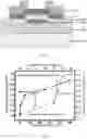
FIG. 1 shows a sectional schematic view of a multi-level cell unit memory structure;
FIG. 2 shows a curve chart of a programming property of a ZnO charge trapping layer-based multi-level cell memory;
FIG. 3 shows a curve chart of an erase property of the ZnO charge trapping layer-based multi-level cell memory; and
FIG. 4 shows a curve chart of a charge retention property of the ZnO charge trapping layer-based multi-level cell memory.
DETAILED DESCRIPTION OF EMBODIMENTS
Hereinafter, the present disclosure will be further described with reference to the preferred embodiments in conjunction with the accompanying drawings. These embodiments are only used for illustrating the present disclosure, not for limiting the protection scope of the present disclosure.
As shown in FIG. 1, the present disclosure provides a multi-level cell thin-film transistor memory, a structure of which memory comprises sequentially from down to top: a gate electrode 10, a charge blocking layer 20, a charge trapping layer 30, a charge tunneling layer 40, an active region 50, and source and drain electrodes 60;
wherein, the charge tunneling layer 40 fully encloses the charge trapping layer 30 so as to completely isolate the charge trapping layer 30 from the ambience; a material of the charge trapping layer 30 is any one of ZnO, In2O3, Ga2O3, SnO2, InSnO, or IGZO.
In an embodiment of the multi-level cell thin-film transistor memory; a material of the gate electrode 10 is P-type single crystal silicon wafer, glass, or PI felxible substrate.
In an embodiment of the multi-level cell thin-film transistor memory, a resistivity of the P-type single crystal silicon wafer is 0.001˜0.005 Ω·cm.
In an embodiment of the multi-level cell thin-film transistor memory, a material of the charge blocking layer 20 is Al2O3, SiO2, HfO2 or ZrO2.
In an embodiment of the multi-level cell thin-film transistor memory, a material of the charge tunneling layer 40 is Al2O3, SiO2, HfO2 or ZrO2.
In an embodiment of the multi-level cell thin-film transistor memory, a material of the active region 50 is IGZO.
In an embodiment of the multi-level cell thin-film transistor memory; a material of the source and drain electrodes 60 is Ti/Au or Mo,
The present disclosure further provides a method of fabricating the multi-level cell thin-film transistor memory, comprising:
Step 1: fabricating a gate electrode 10;
Step 2: growing a charge blocking layer 20 on the gate electrode 10 resulting from step 1 by atomic layer deposition, wherein a thickness of the charge blocking layer 20 is 30˜60 nm and its deposition temperature is 150˜350° C.
Step 3: growing a charge trapping layer 30 on the charge blocking layer 20 resulting from step 2 by atomic deposition or magnetic sputtering deposition. Wherein a thickness of the charge trapping layer 30 is 10˜40 nm.
Step 4: spin coating a layer of positive photoresist on the charge trapping layer 30 resulting from step 3; then performing photolithography to define a region of the charge trapping layer 30; and next, removing portions beyond the defined charge trapping layer 30 region by wet etching;
Step 5: growing a charge tunneling layer 40 on the charging trapping layer 30 resulting from step 4 and the exposed charge blocking layer 20 by atomic layer deposition, wherein a thickness of the charge tunneling layer 40 is 6˜15 nm and a deposition temperature is 150˜350° C.
Step 6: growing a layer of IGZO thin film, which serves as an active layer of the memory, on the charge tunneling layer 40 resulting from step 5 by magnetic sputtering deposition; then defining an active region 50 by photolithography and wet etching to form an active channel of the memory, wherein a thickness of the IGZO thin film is 30˜60 nm;
Step 7: spin coating a layer of negative photoresist on the IGZO thin film resulting from step 6; defining pattern regions (opening regions) of source and drain electrodes 60 by photolithography ; then, depositing a layer of metal thin film as a source and drain electrodes 60 material by magnetic sputtering deposition or electron beam evaporation; and removing metal layers beyond the pattern regions of source and drain electrodes 60 by a lift-off process to thereby form source and drain electrodes of the memory, wherein a thickness of the metal thin film is 50˜200 nm;
Step 8: performing subsequent annealing treatment to the memory resulting from step 7, wherein an annealing atmosphere is oxygen or air, and an annealing temperature is 150˜350° C., and an annealing duration is 60 s˜2 h;
In the method of fabricating the multi-level cell thin-film transistor memory, the step 1 specifically comprises: with the P-type single crystal silicon wafer as a substrate, forming the gate electrode 10 by standard cleaning, or with the glass or PI flexible substrate as a substrate, depositing a layer of metal thereon and forming the gate electrode 10 by photolithography and etching.
Embodiment I
This embodiment utilizes ZnO thin film as the charge trapping layer 30, a specific fabrication process thereof comprising:
Step 1: with a P-type single crystal silicon wafer with a transmittance of 0.001˜0.005 Ω·cm as a substrate, performing RCA cleaning treatment to the substrate to form a gate electrode 10;
Step 2: growing a layer of Al2O3 thin film, which serves as a charge blocking layer 20, on the gate electrode 10 by ALD; the deposition temperature is 15018 350° C., preferably 300° C.; a thickness of the thin film is 30˜60 nm, preferably 35 nm;
Step 3: growing a layer of ZnO thin film, which serves as a charge trapping layer 30, on the charge blocking layer 20 by the ALD method or a PVD method; the deposition temperature is 150˜350° C., preferably 200° C.; the thin film has a thickness of 10˜40 nm, preferably 20 nm;
Step 4: spin coating a layer of positive photoresist on the charge trapping layer 30; then performing exposing and developing to define a region of the charge trapping layer 30 of the memory, and next, removing portions beyond the defined charge trapping layer 30 region using diluted hydrochloric acid;
Step 5: growing, by ALD, a layer of Al2O3 thin film, which serves as a charge tunneling layer 40, on the charge trapping layer 30 and the charge blocking layer 20 which is exposed after being etched with the diluted hydrochloric acid, wherein the deposition temperature is 150˜350° C., preferably 300° C.; and a thickness of the thin film is 6˜15 nm, preferably 8 nm;
Step 6: growing a layer of IGZO thin film, which serves as an active layer, on the charge tunneling layer 40 by PVD, wherein an atomic ratio in an IGZO target material is In:Ga:Zn:O=1:1:1:4, a sputtering power is 110 W, a working pressure is 0.88 Pa, and the fluxes of Ar and O2 introduced in a deposition chamber are 50 sccm and 0 sccm, respectively; and defining an active region 50 by photolithography and wet etching to form an active channel of the memory, wherein a thickness of the IGZO thin film is 30˜60 nm, preferably 40 nm;
Step 7: spin coating a layer of negative photoresist on the IGZO thin film; defining pattern regions (opening regions) of source and drain electrodes 60 by photolithography; then, blanket depositing a layer of Ti/AU dual-layer metal thin film as a source and drain electrodes 60 material by magnetic sputtering deposition or electron beam evaporation, wherein the thickness of the metal thin film is 50˜200 nm, preferably 100 nm; then, removing metal layers beyond the pattern regions of source and drain electrodes 60 by a lift-off process to thereby form source and drain electrodes 60 of the memory;
Step 8: performing subsequent annealing treatment to the memory, therein annealing atmosphere is oxygen (O2), an annealing temperature is 150˜350° C., preferably 250° C.; and an annealing duration is 60˜600 s, preferably 300 s.
FIG. 2 shows a programming property of the memory fabricated in Embodiment I. When the programming voltage is fixed at 12V and the programming duration increases from 0.001 ms to 100 ms, the programming window (a difference between the programmed threshold voltage and the initial-state threshold voltage) increases from 1.47 V to 2.75 V; when the fixed programming duration is 10 ms and the programming voltage increases from 10V to 16V, the programming window increases from 1.89V to 3.44V This indicates that the memory has a good programming property. FIG. 3 shows an erase property of the memory fabricated in Embodiment I. When the erase voltage is fixed at −8V and the erase duration increases from 1 μs to 70 μs, the erase window (a difference between the erase threshold voltage and the initial-state threshold voltage) increases from 2V to 4.99V; when the fixed erase duration is 10 ms and the erase voltage increases from −8V to −14V, the erase window increases from 2V to 8.5V. This indicates that the memory fabricated in Embodiment I has a very high electrical erase efficiency.
By changing a bias pulse on the gate, four states may be realized, i.e., “00,” “11,” “10,” and “01” states. Here, the memory initial state is defined as “00” state; the memory programming state is defined as “11” state (e.g., 1.5V/10 ms); a low negative bias pulse (e.g., −8V/10 μs) erase state is defined as “10”; and a high negative bias pulse (e.g., −14 V/1 μs) erase state is defined as “01” state. FIG. 4 shows charge retention properties under different storage states of the memory fabricated in Embodiment I. The operation condition of the “11” state is 15V/10 ms; the operation state of the “00” state is the memory initial state; and the operation conditions of “10” state and “01” state are −8 V/10 μs and −14 V/1 μs, respectively. It may be seen from FIG. 1 that when the retention time reaches 105 s, the storage window of the memory from “11” state to “00” state is 2V; the storage window from the “00” state to “10” state is 1.1V; and the storage window from the “10” state to the “01” state is 1.6V. This enables the memory to normally distinguish the four different storage states of “00, ” “11, ” “10,” and “01.”
Embodiment II
This embodiment utilizes IGZO thin film as the charge trapping layer 30, a specific fabrication process thereof comprising:
Step 1: with a P-type single crystal silicon wafer with a transmittance of 0.001˜0.005 Ω·cm as a substrate, performing RCA cleaning treatment to the substrate to form a gate electrode 10;
Step 2: growing a layer of Al2O3 thin film, which serves as a charge blocking layer 20, on the gate electrode 10 by ALD the deposition temperature is 150˜350° C., preferably 300° C.; a thickness of the thin film is 30˜60 nm, preferably 35 nm;
Step 3: growing a layer of IGZO thin film, which serves as a charge trapping layer 30, on the charge blocking layer 20 by PVD, wherein an atomic ratio in an IGZO target material is In:Ga:Zn:O=1:1:1:4, a sputtering power is 110 W, a working pressure is 0.88 Pa, and the fluxes of Ar and O2 introduced in a deposition chamber are 50 sccm and 0 sccm, respectively; wherein the thickness of the IGZO thin film is 10˜40 nm, preferably 20 nm;
Step 4: spin coating a layer of positive photoresist on the charge trapping layer 30; then performing exposing and developing to define a region of the charge trapping layer 30 of the memory, and next, removing portions beyond the defined charge trapping layer 30 region using diluted hydrochloric acid;
Step 5: growing, by ALD, a layer of Al2O3 thin film, which serves as a charge tunneling layer 40, on the charge trapping layer 30 and the charge blocking layer 20 which is exposed after being etched with the diluted hydrochloric acid; the deposition temperature is 150˜350° C., preferably 300° C.; a thickness of the thin film is 6˜15 nm, preferably 8 nm;
Step 6: growing a layer of IGZO thin film, which serves as an active layer, on the charge tunneling layer 40 by PVD, wherein an atomic ratio in an IGZO target material is In:Ga:Zn:O=1:1:1:4, a sputtering power is 110 W, a working pressure is 0.88 Pa, and the fluxes of Ar and O2 introduced in a deposition chamber are 50 sccm and 0 sccm, respectively; defining an active region 50 by photolithography and wet etching to form an active channel of the memory, wherein the thickness of the IGZO thin film is 30˜60 nm, preferably 40 nm;
Step 7: spin coating a layer of negative photoresist on the IGZO thin film; defining pattern regions (opening regions) of source and drain electrodes 60 by photolithography; then, blanket depositing a layer of Mo metal thin film as a source and drain electrodes 60 material by magnetic sputtering deposition or electron beam evaporation, wherein the thickness of the metal thin film is 50˜200 nm, preferably 100 nm; then, removing metal layers beyond the pattern regions of source and drain electrodes 60 by a lift-off process to thereby form source and drain electrodes 60 of the memory;
Step 8: performing subsequent annealing treatment to the memory, wherein an annealing atmosphere is air, an annealing temperature is 150˜350° C., preferably 300° C., and an annealing duration is 0.5˜2 h, preferably 1 h.
By performing different voltage programming to the memory fabricated in Embodiment 2, different states may be implemented. For example, when a 12V 10 ms pulse is applied to the gate, the memory changes from the initial state to the programming state; besides, the two states may he mutually converted (wherein the voltage pulse condition for restoring the initial state is −12V, 20 ms); when a −15V 10 ms pulse is applied to the gate, the memory changes from the initial state to the erase state; besides, the two states may also be mutually converted (wherein the voltage pulse condition for restoring the initial state is 11V, 15 ms). Table 1 lists retention properties of the memory fabricated in Embodiment II under different states. As the retention duration extends from 0 second to 105 seconds, the threshold voltages (Vth) of the programming state, initial state, and erase state change from 2.276 V, −0.09 V, −2.4 V to 1.574 V, −0.339 V, −1.634 V, respectively, which reflect a good stability.
| TABLE 1 |
| Retention Properties of ZnO Charge Trapping |
| Layer-Based Multi-Level Cell |
| Programming State | Initial State | Erase State | |
| Threshold Voltage | Threshold | Threshold | |
| (Vth) | Voltage (Vth) | Voltage (Vth) | |
| Gate Voltage | 12 V, 10 ms | N/A | −15 V, 10 ms |
| Pulse | |||
| 0 Second | Vth = 2.276 V | Vth = −0.09 V | Vth = −2.4 V |
| 105 seconds | Vth = 1.574 V | Vth = −0.339 V | Vth = −1.634 V |
In view of the above, as the charging trapping layer of the thin-film transistor memory fabricated according to the present disclosure is fully enclosed by the charging tunneling layer, the former may be completely isolated from the ambiance, which prevents change of physical properties and chemical compositions of the charge trapping layer during the processing process, reduces loss of charges stored in the charge trapping layer, and enhances data retention property and memory performance stability; the present disclosure utilizes a metal oxide semiconductor thin film as the charge trapping layer of the memory, which implements multi-level cell storage and improves storage density; the thin-film transistor memory fabricated according to the present disclosure may be fabricated under a temperature lower than 350° C., which lowers the thermal budget of memory fabrication; besides, the fabrication process is compatible with the thin-film transistor process. Further, as the IGZO thin film has a relatively high visible light transmissivity, the present disclosure has a wide application prospect in fields such as future SoPs and flexible transparent electronic devices.
Although the contents of the present disclosure have been described in detail through the foregoing preferred embodiments, it should be understood that the depictions above shall not be regarded as limitations to the present disclosure. After those skilled in the art having read the contents above, many modifications and substitutions to the present disclosure are all obvious. Therefore, the protection scope of the present disclosure should be limited by the appended claims.
Claims
1. A multi-level cell thin-film transistor memory, a structure of which memory comprises sequentially from down to top: a gate electrode, a charge blocking layer, a charge trapping layer, a charge tunneling layer, an active region, and source and drain electrodes; the memory is fabricated by annealing treatment;
wherein, the charge tunneling layer fully encloses the charge trapping layer so as to completely isolate the charge trapping layer from the ambience to prevent change of physical properties and chemical compositions of the charge trapping layer during the annealing treatment and reduce loss of charges stored in the charge trapping layer; a material of the charge trapping layer is any one of ZnO, In2O3, Ga2O3, SnO2, InSnO, or IGZO (amorphous indium gallium zinc oxide).
2. The multi-level cell thin-film transistor memory according to claim 1, wherein a material of the gate electrode is P-type single crystal silicon wafer, glass, or PI flexible substrate.
3. The multi-level cell thin-film transistor memory according to claim 2,
wherein a resistivity of the P-type single crystal silicon wafer is 0.001˜0.005 Ω·cm.
4. The multi-level cell thin-film transistor memory according to claim 1,
wherein a material of the charge blocking layer is Al2O3, SiO2, HfO2 or ZrO2.
5. The multi-level cell thin-film transistor memory according to claim 1,
wherein a material of the charge tunneling layer is Al2O3, SiO2, HfO2 or ZrO2.
6. The multi-level cell thin-film transistor memory according to claim 1,
wherein a material of the active region is IGZO.
7. The multi-level cell thin-film transistor memory according to claim 1,
wherein a material of the source and drain electrodes is Ti/Au or Mo.
8. A method of fabricating the multi-level cell thin-film transistor memory, comprising:
Step 1: fabricating a gate electrode;
Step 2: growing a charge blocking layer on the gate electrode resulting from step 1 by atomic layer deposition, wherein a thickness of the charge blocking layer is 30˜60 nm and its deposition temperature is 150˜350° C.;
Step 3: growing a charge trapping layer on the charge blocking layer resulting from step 2 by atomic deposition or magnetic sputtering deposition, wherein a thickness of the charge trapping layer is 10˜40 nm.
Step 4: spin coating a layer of positive photoresist on the charge trapping layer resulting from step 3; then performing photolithography (exposing and developing) to define a region of the charge trapping layer; and next, removing portions beyond the defined charge trapping layer region by wet etching;
Step 5: growing a charge tunneling layer on the charging trapping layer resulting from step 4 and the exposed charge blocking layer by atomic layer deposition, wherein a thickness of the charge tunneling layer is 6˜15 nm and a deposition temperature is 150˜350° C.
Step 6: growing a layer of IGZO thin film, which serves as an active layer of the memory, on the charge tunneling layer resulting from step 5 by magnetic sputtering deposition, then defining an active region by photolithography and wet etching to form an active channel of the memory, wherein a thickness of the IGZO thin film is 30˜60 nm;
Step 7: spin coating a layer of negative photoresist on the IGZO thin film resulting from step 6; defining pattern regions of source and drain electrodes by photolithography; then, depositing a layer of metal thin film as a source and drain electrodes material by magnetic sputtering deposition or electron beam evaporation, and removing metal layers beyond the pattern regions of source and drain electrodes by a lift-off process to thereby form source and drain electrodes of the memory, wherein a thickness of the metal thin film is 50˜200 nm.
Step 8: performing subsequent annealing treatment to the memory resulting from step 7, wherein an annealing atmosphere is oxygen or air, and an annealing temperature is 150˜350° C., and an annealing duration is 60 s˜2 h.
9. The method of fabricating the multi-level cell thin-film transistor memory according to claim 8, wherein the step 1 specifically comprises: with the P-type single crystal silicon wafer as a substrate, performing standard cleaning treatment to form the gate electrode, or with the glass or PI flexible substrate as a substrate, depositing a layer of metal thereon and forming the gate electrode by photolithography and etching.
Images & Drawings included:


Sources:
- United States Patent and Trademark Office - verify current appl. status at the USPTO↗
Recent applications in this class:
- » 20240114688 2024-04-04
MEMORY STRUCTURE AND MANUFACTURING METHOD THEREOF - » 20240107771 2024-03-28
Method of forming oxide-nitride-oxide stack of non-volatile memory and integration to CMOS process flow - » 20240049470 2024-02-08
MEMORY CELL ARRAY WITH INCREASED SOURCE BIAS VOLTAGE - » 20230413564 2023-12-21
Memory storage device and method of manufacturing the same - » 20230309309 2023-09-28
SONOS memory cell structure and fabricating method of the same - » 20230200075 2023-06-22
MEMORY WITH VERTICAL TRANSISTORS AND WRAP-AROUND CONTROL LINES - » 20230109273 2023-04-06
Integrated chip including a tunnel dielectric layer which has different thicknesses over a protrusion region of a substrate - » 20230100464 2023-03-30
Memory structure and manufacturing method for the same - » 20230067382 2023-03-02
Integrated chip with a gate structure disposed within a trench - » 20230046058 2023-02-16
Memory structure
Recent applications for this Assignee:
- » 20250236538 2025-07-24
Ammonia-driven hydrogel dehydration-desalination method - » 20250215598 2025-07-03
LEVELING AGENT, COMPOSITION, AND APPLICATION THEREOF - » 20250205304 2025-06-26
CD300LD INHIBITOR AND USE THEREOF IN THE PREPARATION OF TUMOR IMMUNOTHERAPY PRODUCTS - » 20250163107 2025-05-22
FUSION PROTEIN AND USE THEREOF - » 20250154146 2025-05-15
PROTEIN DEGRADERS DEVELOPED ON BASIS OF BCL-2 FAMILY PROTEIN LIGAND COMPOUNDS AND USE THEREOF - » 20250115941 2025-04-10
Exposure device for exposing microorganisms to gaseous pollutants and detection system thereof - » 20250115894 2025-04-10
Three-dimensional model of exposed microbial membranes at gas-liquid interface and preparation method thereof - » 20250060344 2025-02-20
Semi-online analytical apparatus for measuring atmospheric trace nitrogen-containing organic components - » 20250059120 2025-02-20
VISIBLE-LIGHT-MEDIATED ONE-STEP METHOD FOR PREPARING PHENOL AND CYCLOHEXANONE FROM CYCLOHEXYLBENZENE - » 20250040196 2025-01-30
FIN FIELD-EFFECT TRANSISTOR DEVICE WITH HYBRID CONDUCTION MECHANISM