Mixed trench junction barrier Schottky diode and method fabricating same
US20200119158A1
2020-04-16
16/161,379
2018-10-16
✅ Patent granted
US 10,672,883 B2
2020-06-02
-
-
Caridad Everhart
Che-Yang Chen | Law Office of Michael Chen
2038-10-16
Abstract:
A method for manufacturing a SiC mixed trench Schottky diode may include steps of providing a substrate and an epitaxial layer on top of the substrate; forming a plurality of trenches on a surface of the epitaxial layer; conducting ion implantation at a bottom portion of each trench; conducting ion implantation at sidewalls of each trench; forming an ohmic contact metal at a bottom portion of the Schottky diode; forming a Schottky contact metal on top of the epitaxial layer and in the trenches. In one embodiment, the substrate is an N+ type SiC and the epitaxial layer is an N− type SiC. In another embodiment, the step of forming a plurality of trenches on a surface of the epitaxial layer may include the step of etching the surface of the epitaxial layer by either dry etching or wet etching.
Inventors:
- NA REN 12 🇺🇸 LOS ANGELES, CA, United States
- ZHENG ZUO 22 🇺🇸 LOS ANGELES, CA, United States
- RUIGANG LI 24 🇺🇸 LOS ANGELES, CA, United States
Assignee:
- AZ Power, Inc 28 🇺🇸 CULVER CITY, CA, United States
Applicant:
Interested in similar patents?
Get notified when new applications in this technology area are published.
Classification:
H01L29/6606 » CPC main
Semiconductor devices adapted for rectifying, amplifying, oscillating or switching, or capacitors or resistors with at least one potential-jump barrier or surface barrier, e.g. PN junction depletion layer or carrier concentration layer; Details of semiconductor bodies or of electrodes thereof; Multistep manufacturing processes therefor; Types of semiconductor device ; Multistep manufacturing processes therefor; Multistep manufacturing processes of devices having a semiconductor body comprising crystalline silicon carbide the devices being controllable only by variation of the electric current supplied or the electric potential applied, to one or more of the electrodes carrying the current to be rectified, amplified, oscillated or switched, e.g. two-terminal devices
H01L21/046 » CPC further
Processes or apparatus adapted for the manufacture or treatment of semiconductor or solid state devices or of parts thereof; Manufacture or treatment of semiconductor devices or of parts thereof the devices having at least one potential-jump barrier or surface barrier, e.g. PN junction, depletion layer or carrier concentration layer the devices having semiconductor bodies comprising crystalline silicon carbide; Making n or p doped regions or layers, e.g. using diffusion using ion implantation
H01L21/0485 » CPC further
Processes or apparatus adapted for the manufacture or treatment of semiconductor or solid state devices or of parts thereof; Manufacture or treatment of semiconductor devices or of parts thereof the devices having at least one potential-jump barrier or surface barrier, e.g. PN junction, depletion layer or carrier concentration layer the devices having semiconductor bodies comprising crystalline silicon carbide; Making electrodes Ohmic electrodes
H01L21/0495 » CPC further
Processes or apparatus adapted for the manufacture or treatment of semiconductor or solid state devices or of parts thereof; Manufacture or treatment of semiconductor devices or of parts thereof the devices having at least one potential-jump barrier or surface barrier, e.g. PN junction, depletion layer or carrier concentration layer the devices having semiconductor bodies comprising crystalline silicon carbide; Making electrodes Schottky electrodes
H01L29/167 » CPC further
Semiconductor devices adapted for rectifying, amplifying, oscillating or switching, or capacitors or resistors with at least one potential-jump barrier or surface barrier, e.g. PN junction depletion layer or carrier concentration layer; Details of semiconductor bodies or of electrodes thereof; Multistep manufacturing processes therefor; Semiconductor bodies ; Multistep manufacturing processes therefor characterised by the materials of which they are formed including, apart from doping materials or other impurities, only elements of Group IV of the Periodic System further characterised by the doping material
H01L29/1608 » CPC further
Semiconductor devices adapted for rectifying, amplifying, oscillating or switching, or capacitors or resistors with at least one potential-jump barrier or surface barrier, e.g. PN junction depletion layer or carrier concentration layer; Details of semiconductor bodies or of electrodes thereof; Multistep manufacturing processes therefor; Semiconductor bodies ; Multistep manufacturing processes therefor characterised by the materials of which they are formed including, apart from doping materials or other impurities, only elements of Group IV of the Periodic System Silicon carbide
H01L29/417 » CPC further
Semiconductor devices adapted for rectifying, amplifying, oscillating or switching, or capacitors or resistors with at least one potential-jump barrier or surface barrier, e.g. PN junction depletion layer or carrier concentration layer; Details of semiconductor bodies or of electrodes thereof; Multistep manufacturing processes therefor; Electrodes ; Multistep manufacturing processes therefor characterised by their shape, relative sizes or dispositions carrying the current to be rectified, amplified or switched
H01L29/66143 » CPC further
Semiconductor devices adapted for rectifying, amplifying, oscillating or switching, or capacitors or resistors with at least one potential-jump barrier or surface barrier, e.g. PN junction depletion layer or carrier concentration layer; Details of semiconductor bodies or of electrodes thereof; Multistep manufacturing processes therefor; Types of semiconductor device ; Multistep manufacturing processes therefor; Multistep manufacturing processes of devices having semiconductor bodies comprising group 14 or group 13/15 materials the devices being controllable only by variation of the electric current supplied or the electric potential applied, to one or more of the electrodes carrying the current to be rectified, amplified, oscillated or switched, e.g. two-terminal devices; Diodes Schottky diodes
H01L29/872 » CPC further
Semiconductor devices adapted for rectifying, amplifying, oscillating or switching, or capacitors or resistors with at least one potential-jump barrier or surface barrier, e.g. PN junction depletion layer or carrier concentration layer; Details of semiconductor bodies or of electrodes thereof; Multistep manufacturing processes therefor; Types of semiconductor device ; Multistep manufacturing processes therefor controllable only by variation of the electric current supplied, or only the electric potential applied, to one or more of the electrodes carrying the current to be rectified, amplified, oscillated or switched; Diodes Schottky diodes
H01L21/02 IPC
Processes or apparatus adapted for the manufacture or treatment of semiconductor or solid state devices or of parts thereof Manufacture or treatment of semiconductor devices or of parts thereof
H01L21/04 IPC
Processes or apparatus adapted for the manufacture or treatment of semiconductor or solid state devices or of parts thereof; Manufacture or treatment of semiconductor devices or of parts thereof the devices having at least one potential-jump barrier or surface barrier, e.g. PN junction, depletion layer or carrier concentration layer
H01L29/06 IPC
Semiconductor devices adapted for rectifying, amplifying, oscillating or switching, or capacitors or resistors with at least one potential-jump barrier or surface barrier, e.g. PN junction depletion layer or carrier concentration layer; Details of semiconductor bodies or of electrodes thereof; Multistep manufacturing processes therefor; Semiconductor bodies ; Multistep manufacturing processes therefor characterised by their shape; characterised by the shapes, relative sizes, or dispositions of the semiconductor regions ; characterised by the concentration or distribution of impurities within semiconductor regions
H01L29/66 IPC
Semiconductor devices adapted for rectifying, amplifying, oscillating or switching, or capacitors or resistors with at least one potential-jump barrier or surface barrier, e.g. PN junction depletion layer or carrier concentration layer; Details of semiconductor bodies or of electrodes thereof; Multistep manufacturing processes therefor Types of semiconductor device ; Multistep manufacturing processes therefor
H01L29/16 IPC
Semiconductor devices adapted for rectifying, amplifying, oscillating or switching, or capacitors or resistors with at least one potential-jump barrier or surface barrier, e.g. PN junction depletion layer or carrier concentration layer; Details of semiconductor bodies or of electrodes thereof; Multistep manufacturing processes therefor; Semiconductor bodies ; Multistep manufacturing processes therefor characterised by the materials of which they are formed including, apart from doping materials or other impurities, only elements of Group IV of the Periodic System
Description
FIELD OF THE INVENTION
The present invention relates to a Schottky diode, and more particularly to a mixed trench type junction barrier Scthottky diode.
BACKGROUND OF THE INVENTION
Silicon carbide (SiC) diodes have been widely recognized for their significant advantages in power applications, especially under high voltage/temperature conditions. In general, SiC Schottky diodes are advantageous because of low onset voltage (as compared with that of SiC p-n diodes) and no reverse recovery. However, reverse leakage current of a planar Schottky diode can be significantly larger under high blocking voltage, caused by tunneling effects at the Schottky interface.
Junction barrier Schottky (JBS) diode structure was proposed to address this problem, which combines the advantages of Schottky junction and PN junction diodes. In JBS structure, a plurality of P regions are disposed between Schottky regions. The depletion layer diffuses from PN junction to exhibit pinch-off below the Schottky contact in reverse blocking mode, which can provide an electric field shielding effect. As a result, the electric field strength at the Schottky interface can be reduced and the diode leakage current can be decreased accordingly.
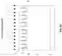
The electric field shielding effect can be enhanced by increasing the PN junction depth. However, due to the strong lattice of SiC material, the ion implantation depth is usually restricted to less than 1 μm. Recently, a trench type junction barrier Schottky diode structure with trenches totally surrounded by P regions is proposed as shown in FIG. 4. With the introduction of the trench, P-type ions can be implanted into the sidewall and bottom of the trench, and the resulting PN junction can be deeper than 1 μm. However, the channel resistance between adjacent deep P regions will be increased since only the upper Schottky contact between the P regions can conduct current in the normal forward manner. As a result, the forward performance of the device will be sacrificed. Therefore, there remains a need for a new and improved trench type junction barrier Schottky diode to overcome the problems stated above.
SUMMARY OF THE INVENTION
In one aspect, a SiC mixed trench junction barrier Schottky diode may include a substrate, an epitaxial layer, a plurality of trenches, a P-type implant, a first Schottky contact metal, an ohmic contact metal, an N-type implant, and a second Schottky contact metal.
In one embodiment, the ohmic contact metal can be nickel, silver or platinum. The substrate 1 produced from N+ type SiC is disposed on the top of the ohmic contact metal, and the epitaxial layer produced from N− type SiC can be disposed on top of the substrate. The trench can be produced by etching the epitaxial layer. In one embodiment, the etching can be done by either dry etching or wet etching. The depth of the trench is about 1 to 50000 angstrom.
The P-type implant is produced by ion implantation into a bottom portion of the trench with P-type materials such as boron or aluminum. In one embodiment, the thickness of the implant is about 1 to 10000 angstrom. The N-type implant is produced by ion implantation into the trench sidewall from N-type material such as nitrogen or phosphorus. In one embodiment, the thickness of the implant is also about 1 to 10000 angstrom.
The first Schottky contact metal is located on top of the epitaxial layer and a Schottky junction can be formed between the first Schottky contact metal and the epitaxial layer. The second Schottky contact metal is filled into the trench. A Schottky junction can be formed between the trench and the epitaxial layer.
In another aspect, a method for manufacturing a SiC mixed trench Schottky diode may include steps of providing a substrate and an epitaxial layer on top of the substrate; forming a plurality of trenches on a surface of the epitaxial layer; conducting ion implantation at a bottom portion of each trench; conducting ion implantation at sidewalls of each trench; forming an ohmic contact metal at a bottom portion of the Schottky diode; forming a Schottky contact metal on top of the epitaxial layer and in the trenches.
In one embodiment, the substrate is an N+ type SiC and the epitaxial layer is an N− type SiC. In another embodiment, the step of forming a plurality of trenches on a surface of the epitaxial layer may include the step of etching the surface of the epitaxial layer by either dry etching or wet etching. The depth of the trench 3 is about 1 to 50000 angstrom.
In a further embodiment, the step of conducting ion implantation at a bottom portion of each trench may include a step of implanting P-type materials such as boron or aluminum into the bottom portion of the trench. The thickness of the P-type implant is about 1 to 10000 angstrom In still a further embodiment, the step of conducting ion implantation at sidewalls of each trench may include a step of implanting N-type materials such as nitrogen or phosphorus into at the sidewalls of the trench. The thickness of the N-type implant is about 1 to 10000 angstrom
BRIEF DESCRIPTION OF THE DRAWINGS
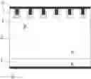
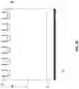
FIG. 1 is a cross-sectional view of a SiC mixed trench junction barrier Schottky diode in the present invention.
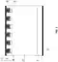
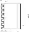
FIGS. 2A-2B illustrates a cross-sectional view of a plurality of trenches on the surface of the epitaxial layer of the SiC mixed trench junction barrier Schottky diode in the present invention.
FIG. 2C illustrates a cross-sectional view of implantation at the bottom portion of each trench of the SiC mixed trench junction barrier Schottky diode in the present invention.
FIG. 2D illustrates a cross-sectional view of implantation at the sidewalls of each trench of the SiC mixed trench junction barrier Schottky diode in the present invention.
FIG. 2E illustrates a cross-sectional view of the trenches after implantation of the SiC mixed trench junction barrier Schottky diode in the present invention.
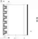
FIGS. 2F-2J illustrate a process flow of forming a Schottky contact metal in the trenches and on the top surface of the SiC mixed trench junction barrier Schottky diode in the present invention.
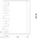
FIG. 3 illustrates a method for manufacturing a SiC mixed trench Schottky diode in the present invention.
FIG. 4 is a prior art.
DETAILED DESCRIPTION OF THE INVENTION
The detailed description set forth below is intended as a description of the presently exemplary device provided in accordance with aspects of the present invention and is not intended to represent the only forms in which the present invention may be prepared or utilized. It is to be understood, rather, that the same or equivalent functions and components may be accomplished by different embodiments that are also intended to be encompassed within the spirit and scope of the invention.
Unless defined otherwise, all technical and scientific terms used herein have the same meaning as commonly understood to one of ordinary skill in the art to which this invention belongs. Although any methods, devices and materials similar or equivalent to those described can be used in the practice or testing of the invention, the exemplary methods, devices and materials are now described.
All publications mentioned are incorporated by reference for the purpose of describing and disclosing, for example, the designs and methodologies that are described in the publications that might be used in connection with the presently described invention. The publications listed or discussed above, below and throughout the text are provided solely for their disclosure prior to the filing date of the present application. Nothing herein is to be construed as an admission that the inventors are not entitled to antedate such disclosure by virtue of prior invention.
As used in the description herein and throughout the claims that follow, the meaning of “a”, “an”, and “the” includes reference to the plural unless the context clearly dictates otherwise. Also, as used in the description herein and throughout the claims that follow, the terms “comprise or comprising”, “include or including”, “have or having”, “contain or containing” and the like are to be understood to be open-ended, i.e., to mean including but not limited to. As used in the description herein and throughout the claims that follow, the meaning of “in” includes “in” and “on” unless the context clearly dictates otherwise.
It will be understood that, although the terms first, second, etc. may be used herein to describe various elements, these elements should not be limited by these terms. These terms are only used to distinguish one element from another. For example, a first element could be termed a second element, and, similarly, a second element could be termed a first element, without departing from the scope of the embodiments. As used herein, the term “and/or” includes any and all combinations of one or more of the associated listed items.
In one aspect, referring to FIGS. 1 and 2A to 2J for a cross sectional view of a SiC mixed trench junction barrier Schottky diode, which may include a substrate 1, an epitaxial layer 2, a plurality of trenches 3, a P-type implant 4, a first Schottky contact metal 5, an ohmic contact metal 6, an N-type implant 8, and a second Schottky contact metal 9.
In one embodiment, the ohmic contact metal 6 can be nickel, silver or platinum. The substrate 1 produced from N+ type SiC is disposed on the top of the ohmic contact metal 6, and the epitaxial layer 2 produced from N− type SiC can be disposed on top of the substrate 1. The trench 3 can be produced by etching the epitaxial layer 2. In one embodiment, the etching can be done by either dry etching or wet etching. The depth of the trench 3 is about 1 to 50000 angstrom.
The P-type implant 4 is produced by ion implantation into a bottom portion of the trench 3 with P-type materials such as boron or aluminum. In one embodiment, the thickness of the implant 4 is about 1 to 10000 angstrom. The N-type implant 8 is produced by ion implantation into the trench sidewall from N-type material such as nitrogen or phosphorus. In one embodiment, the thickness of the implant 8 is also about 1 to 10000 angstrom.
The first Schottky contact metal 5 is located on top of the epitaxial layer 2 and a Schottky junction can be formed between the first Schottky contact metal 5 and the epitaxial layer 2. The second Schottky contact metal 9 is filled into the trench 3. A Schottky junction can be formed between the trench 3 and the epitaxial layer 2.
In another aspect, as shown in FIG. 3, a method for manufacturing a SiC mixed trench Schottky diode may include steps of providing a substrate and an epitaxial layer on top of the substrate 310; forming a plurality of trenches on a surface of the epitaxial layer 320; conducting ion implantation at a bottom portion of each trench 330; conducting ion implantation at sidewalls of each trench 340; forming an ohmic contact metal at a bottom portion of the Schottky diode 350; forming a Schottky contact metal on top of the epitaxial layer and in the trenches 360.
In one embodiment, the substrate is an N+ type SiC and the epitaxial layer is an N− type SiC. In another embodiment, the step of forming a plurality of trenches on a surface of the epitaxial layer may include the step of etching the surface of the epitaxial layer by either dry etching or wet etching. The depth of the trench 3 is about 1 to 50000 angstrom.
In a further embodiment, the step of conducting ion implantation at a bottom portion of each trench may include a step of implanting P-type materials such as boron or aluminum into the bottom portion of the trench. The thickness of the P-type implant is about 1 to 10000 angstrom In still a further embodiment, the step of conducting ion implantation at sidewalls of each trench may include a step of implanting N-type materials such as nitrogen or phosphorus into at the sidewalls of the trench. The thickness of the N-type implant is about 1 to 10000 angstrom. In still a further embodiment, the ohmic contact metal in step 350 can be nickel, silver or platinum.
Having described the invention by the description and illustrations above, it should be understood that these are exemplary of the invention and are not to be considered as limiting. Accordingly, the invention is not to be considered as limited by the foregoing description, but includes any equivalent.
Claims
What is claimed is:1. A method for manufacturing a SiC mixed trench Schottky diode comprising:
providing a substrate and an epitaxial layer on top of the substrate;
forming a plurality of trenches on a surface of the epitaxial layer;
conducting ion implantation at a bottom portion of each trench;
conducting ion implantation at sidewalls of each trench;
forming an ohmic contact metal at a bottom portion of the Schottky diode;
forming a Schottky contact metal on top of the epitaxial layer and in the trenches.
2. The method for manufacturing a SiC mixed trench Schottky diode of claim 1, wherein the substrate is an N+ type SiC.
3. The method for manufacturing a SiC mixed trench Schottky diode of claim 1, wherein the epitaxial layer is an N− type SiC.
4. The method for manufacturing a SiC mixed trench Schottky diode of claim 1, wherein the step of forming a plurality of trenches on a surface of the epitaxial layer may include a step of etching the surface of the epitaxial layer by either dry etching or wet etching.
5. The method for manufacturing a SiC mixed trench Schottky diode of claim 4, wherein a depth of each trench is about 1 to 50000 angstrom.
6. The method for manufacturing a SiC mixed trench Schottky diode of claim 1, wherein the step of conducting ion implantation at a bottom portion of each trench may include a step of implanting P-type materials such as boron or aluminum into the bottom portion of the trench.
7. The method for manufacturing a SiC mixed trench Schottky diode of claim 6, wherein a thickness of the P-type implant is about 1 to 10000 angstrom
8. The method for manufacturing a SiC mixed trench Schottky diode of claim 1, wherein the step of conducting ion implantation at sidewalls of each trench may include a step of implanting N-type materials such as nitrogen or phosphorus into at the sidewalls of the trench.
9. The method for manufacturing a SiC mixed trench Schottky diode of claim 8, wherein a thickness of the N-type implant is about 1 to 10000 angstrom.
10. The method for manufacturing a SiC mixed trench Schottky diode of claim 1, wherein the ohmic contact metal includes nickel, silver and platinum.
11. A SiC mixed trench Schottky diode comprising an ohmic contact metal, a substrate made from N+ SiC located on the top of said ohmic contact metal, an epitaxial layer produced from N− type SiC located on the top of said substrate, a trench produced by etching said epitaxial layer, a P-type implant formed in the bottom of said trench, an N-type implant formed in the side wall of said trench, a Schottky contact metal produced from a metal located on the top of said epitaxial layer, a Schottky junction being produced between said Schottky contact metal and said epitaxial layer, a second Schottky contact metal produced by a second metal filled into said trench, for the purpose of introduce an additional low barrier Schottky junction between said trench layer and said epitaxial layer and a voltage reducing layer made from N-type impurity located in the side wall of said trench.
12. The SiC mixed trench Schottky diode of claim 1, wherein the depth of said trench is about 1 to 50000 angstrom.
13. The SiC mixed trench Schottky diode of claim 1, wherein the material of said P-type implant contains boron.
14. The SiC mixed trench Schottky diode of claim 1, wherein the material of said P-type implant contains aluminum.
15. The SiC mixed trench Schottky diode of claim 1, wherein the material of said N-type implant contains nitrogen.
16. The SiC mixed trench Schottky diode of claim 1, wherein the material of said N-type implant contains phosphorus.
17. The SiC mixed trench Schottky diode of claim 1, wherein the thickness of said N-type implant is about 1 to 10000 angstrom.
Images & Drawings included:


Sources:
- United States Patent and Trademark Office - verify current appl. status at the USPTO↗
Recent applications in this class:
- » 20230299173 2023-09-21
FORMING AN ELECTRONIC DEVICE, SUCH AS A JBS OR MPS DIODE, BASED ON 3C-SIC, AND 3C-SIC ELECTRONIC DEVICE - » 20230087112 2023-03-23
CONTEXTUAL FORMATION OF A JUNCTION BARRIER DIODE AND A SCHOTTKY DIODE IN A MPS DEVICE BASED ON SILICON CARBIDE, AND MPS DEVICE - » 20210226031 2021-07-22
Method of manufacturing silicon carbide semiconductor device - » 20190237558 2019-08-01
SIC SEMICONDUCTOR DEVICE HAVING PN JUNCTION INTERFACE AND METHOD FOR MANUFACTURING THE SIC SEMICONDUCTOR DEVICE - » 20160336423 2016-11-17
METHOD OF MANUFACTURING SILICON CARBIDE SEMICONDUCTOR DEVICE - » 20160247894 2016-08-25
SiC semiconductor device having pn junction interface and method for manufacturing the SiC semiconductor device - » 20160056260 2016-02-25
Method for manufacturing silicon carbide (SiC) semiconductor device by introducing nitrogen concentration of 5X1019 cm-3 or more at a boundary surface between thermal oxide film and the SiC substrate and then removing the thermal oxide film - » 20110248285 2011-10-13
Semiconductor devices including schottky diodes having overlapping doped regions and methods of fabricating same - » 20110117753 2011-05-19
Heat treatment apparatus and semiconductor device manufacturing method - » 20080206924 2008-08-28
METHOD FOR FABTRICATING SEMICONDUCTOR DEVICE
Recent applications for this Assignee:
- » 20230411534 2023-12-21
Merged PiN Schottky (MPS) diode with plasma spreading layer and manufacturing method thereof - » 20220181443 2022-06-09
Power MOSFET With Enhanced Cell Design - » 20210328078 2021-10-21
Merged PiN Schottky (MPS) Diode With Plasma Spreading Layer And Manufacturing Method Thereof - » 20210328077 2021-10-21
Merged PiN Schottky (MPS) Diode With Multiple Cell Designs And Manufacturing Method Thereof - » 20210328076 2021-10-21
Merged PiN Schottky (MPS) diode with plasma spreading layer and manufacturing method thereof - » 20210218348 2021-07-15
THREE-PHASE FULL SiC INVERTER WITH ZERO-VOLTAGE SWITCHING CAPABILITY - » 20210218346 2021-07-15
INVERTER SYSTEM WITH MINIMUM OUTPUT FILTER - » 20210218344 2021-07-15
BOOST INVERTER SYSTEM WITH ENHANCED TOLERANCE FOR LOW VOLTAGE INPUT BUS - » 20210218341 2021-07-15
MULTILEVEL STEP-UP INVERTER BASED ON DISTRIBUTED PASSIVE COMPONENTS - » 20210098579 2021-04-01
SCHOTTKY DIODE WITH HIGH BREAKDOWN VOLTAGE AND SURGE CURRENT CAPABILITY USING DOUBLE P-TYPE EPITAXIAL LAYERS