Crossbar, Inc.
Santa Clara, California
United States
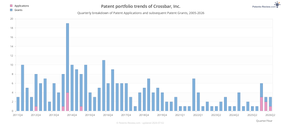
255
2026-06-30
248
2026-06-30
Top Inventors for applications by Crossbar, Inc.
These are the the leading inventors for applications assigned to Crossbar, Inc.:
- Sung Hyun JO 110 Sunnyvale, CA United States
- Hagop Nazarian 85 San Jose, CA United States
- Scott Brad Herner 35 San Jose, CA United States
- Mehdi Asnaashari 33 Danville, CA United States
- Tanmay KUMAR 21 Pleasanton, CA United States
- Sundar NARAYANAN 20 Cupertino, CA United States
- Sang NGUYEN 18 Union City, CA United States
- Wei Lu 14 Ann Arbor, MI United States
- Natividad VASQUEZ, JR. 14 San Francisco, CA United States
- Steven Patrick MAXWELL 13 Sunnyvale, CA United States
- Kuk-Hwan KIM 11 San Jose, CA United States
- Zhi Li 11 Santa Clara, CA United States
- Mark Harold CLARK 11 Santa Clara, CA United States
- Natividad Vasquez 9 San Francisco, CA United States
- Harry Yue GEE 9 Santa Clara, CA United States
- Harry Yue Gee 7 Milpitas, CA United States
- Lin-Shih LIU 7 Fremont, CA United States
- Crossbar, Inc. 7 Santa Clara, CA United States
- Sang Thanh Nguyen 6 Union City, CA United States
- Zhen Gu 6 Cupertino, CA United States
- Crossbar, Inc. 6 , United States
- Joanna BETTINGER 6 Oakland, CA United States
- Xianliang LIU 6 Emeryville, CA United States
- Tianhong Yan 5 Saratoga, CA United States
- FNU Atiquzzaman 5 Berkeley, CA United States
- Steve Maxwell 5 Sunnyvale, CA United States
- Cliff ZITLAW 4 San Jose, CA United States
- Tanmay KUMAR 4 Santa Clara, CA United States
- Jeremy Guy 4 San Jose, CA United States
- Ruchirkumar Shah 4 San Jose, CA United States
- Harry KUO 4 Cupertino, CA United States
- Harry GEE 4 Sunnyvale, CA United States
- Steven Maxwell 3 Sunnyvale, CA United States
- Zeying Ren 3 Albany, CA United States
- Wee-chen Gan 3 Cupertino, CA United States
- Sylvain Dubois 3 San Francisco, CA United States
- Frank EDELHAEUSER 3 Dresden, Germany
- Cung Vu 3 San Jose, CA United States
- Christophe Sucur 3 San Jose, CA United States
- Xu Zhao 3 Richmond, CA United States
- Liang Zhao 3 Santa Clara, CA United States
- George MINASSIAN 3 Santa Clara, CA United States
- Ruchirkumar D. Shah 2 San Jose, CA United States
- Fengchiao Joyce Lin 2 San Jose, CA United States
- Robin Sarno 2 Pleasanton, CA United States
- Chen-Chun CHEN 2 Fremont, CA United States
- Wei Ti Lee 2 San Jose, CA United States
- Layne Armijo 2 Los Gatos, CA United States
- Yunyu Wang 2 San Jose, CA United States
- Ping LU 2 Sunnyvale, CA United States
- Kuk-Hwan KIM 1 Santa Clara, CA United States
- Harry Kuo 1 Palo Alto, CA United States
- Hagop Nazarian 1 Danville, CA United States
- Sang Nguyen 1 Sunnyvale, CA United States
- Ming-Huei SHIEH 1 Cupertino, CA United States
- San Thanh Nguyen 1 Union City, CA United States
- Hagop NAZARIAN 1 San Jose, US United States
- Scott Brad Herner 1 Santa Clara, CA United States
- Derek Lau 1 Santa Clara, CA United States
- Scott Brad Harold 1 San Jose, CA United States
- Dzung Huu Nguyen 1 Fremont, CA United States
- Amit PRAKASH 1 Santa Clara, CA United States
- John Nguyen 1 Milpitas, CA United States
- Sung-Hyun Jo 1 Santa Clara, CA United States
- Jordan Frick 1 San Jose, CA United States
- Xin SUN 1 Albany, CA United States
- Sundar NARAYANAN 1 Santa Clara, CA United States
- Majid Milani 1 San Jose, CA United States
- Tanmay Kumar 1 Pleasaton, CA United States
- Liang Xiao 1 Santa Clara, CA United States
- Harry KUO 1 Cupertino, US United States
Recent patent applications by Crossbar, Inc.
Crossbar, Inc. based in Santa Clara, US has been assigned the rights to these inventions. The list includes both Pending Applications and Patent Grants:
US18676046
ElectricityResistive switching memory having confined filament formation and methods thereof
#2 | 2026-05-12 ✅ Patent 12,626,759 granted on 2026-05-12US18412022
PhysicsError correction for identifier data generated from unclonable characteristics of resistive memory
#3 | 2026-02-10 ✅ Patent 12,549,388 granted on 2026-02-10US18200318
ElectricityUtilizing two-terminal resistive switching memory to store validation data of an integrated circuit device
#4 | 2025-12-16 ✅ Patent 12,499,244 granted on 2025-12-16US18218955
PhysicsParameterized key size for CSP address table mapping in secure microcontroller with unified RRAM
#5 | 2025-12-16 ✅ Patent 12,499,260 granted on 2025-12-16US18218950
PhysicsLink table for characterizing multi-mode CSP parameters in a secure microcontroller with unified RRAM
#6 | 2025-12-02 ✅ Patent 12,488,836 granted on 2025-12-02US18109029
PhysicsMonotonic counter implemented in non-volatile resistive switching memory
#7 | 2025-07-10 ✅ Patent 12,423,681 granted on 2025-09-23US20250225507A1
PhysicsCRYPTOCURRENCY HARDWARE WALLET ON MONOLITHIC CHIP WITH COMMON PHYSICAL COUNTERMEASURES AND SECURE MEMORY
#8 | 2025-04-08 ✅ Patent 12,272,399 granted on 2025-04-08US18587443
PhysicsDifferential programming of two-terminal resistive switching memory with program soaking and adjacent path disablement
#9 | 2025-03-18 ✅ Patent 12,254,124 granted on 2025-03-18US18529596
PhysicsSecure circuit integrated with memory layer
#10 | 2025-01-28 ✅ Patent 12,211,549 granted on 2025-01-28US18596150
PhysicsCell cycling to minimize resistive memory random number correlation
#11 | 2024-11-07 ✅ Patent 12,368,455 granted on 2025-07-22US20240372564A1
ElectricityFLEXIBLE AND CONFIGURABLE BIT ERROR RATE REDUCTION FOR NON-VOLATILE MEMORY
#12 | 2024-09-24 ✅ Patent 12,100,449 granted on 2024-09-24US17710809
PhysicsDifferential programming of two-terminal resistive switching memory with intrinsic error suppression
#13 | 2024-09-12 ✅ Patent 12,437,811 granted on 2025-10-07US20240304243A1
PhysicsERASE ALGORITHM WITH A WEAK PROGRAM PULSE FOR NON-VOLATILE MEMORY
#14 | 2024-09-10 ✅ Patent 12,087,397 granted on 2024-09-10US17708491
PhysicsDynamic host allocation of physical unclonable feature operation for resistive switching memory
#15 | 2024-09-03 ✅ Patent 12,080,347 granted on 2024-09-03US17710835
PhysicsDifferential programming of two-terminal resistive switching memory with program soaking and adjacent path disablement
#16 | 2024-04-04 ✅ Patent 12,166,482 granted on 2024-12-10US20240113715A1
ElectricityGenerating physical unclonable function data from a transistor of a semiconductor device
#17 | 2024-02-29 ✅ Patent 12,198,760 granted on 2025-01-14US20240071490A1
PhysicsDifferential programming of two-terminal memory with intrinsic error suppression and wordline coupling
#18 | 2023-10-05 ✅ Patent 12,154,624 granted on 2024-11-26US20230317162A1
PhysicsDifferential programming of two-terminal memory with program detection and multi-path disablement
#19 | 2023-10-05 ✅ Patent 11,901,003 granted on 2024-02-13US20230317158A1
PhysicsError correction for identifier data generated from unclonable characteristics of resistive memory
#20 | 2023-10-05 ✅ Patent 12,020,748 granted on 2024-06-25US20230317157A1
PhysicsReverse programmed resistive random access memory (RAM) for one time programmable (OTP) applications
#21 | 2023-09-28 ✅ Patent 11,923,005 granted on 2024-03-05US20230307044A1
PhysicsCell cycling to minimize resistive memory random number correlation
#22 | 2023-09-21 ✅ Patent 11,973,500 granted on 2024-04-30US20230299772A1
ElectricityConfiguration bit using RRAM
#23 | 2023-05-18 ✅ Patent 12,245,527 granted on 2025-03-04US20230157186A1
ElectricityNon-stoichiometric resistive switching memory device and fabrication methods
#24 | 2023-01-05 ✅ Patent 11,967,376 granted on 2024-04-23US20230005538A1
PhysicsDistinct chip identifier sequence utilizing unclonable characteristics of resistive memory on a chip
#25 | 2022-10-06 ✅ Patent 11,997,932 granted on 2024-05-28US20220320432A1
ElectricityResistive switching memory having confined filament formation and methods thereof
#26 | 2022-10-06 ✅ Patent 12,075,712 granted on 2024-08-27US20220320429A1
ElectricityResistive switching memory devices and method(s) for forming the resistive switching memory devices
#27 | 2022-07-12 ✅ Patent 11,387,409 granted on 2022-07-12US16688640
ElectricityFormation of structurally robust nanoscale Ag-based conductive structure
#28 | 2022-02-17 ✅ Patent 11,727,986 granted on 2023-08-15US20220051718A1
PhysicsPhysically unclonable function (PUF) generation involving programming of marginal bits
#29 | 2022-02-03 ✅ Patent 11,823,739 granted on 2023-11-21US20220036949A1
PhysicsPhysically unclonable function (PUF) generation involving high side programming of bits
#30 | 2022-01-11 ✅ Patent 11,222,696 granted on 2022-01-11US16917261
PhysicsComputing memory architecture
#31 | 2022-01-06 ✅ Patent 11,393,529 granted on 2022-07-19US20220005527A1
PhysicsCapacitance measurement and apparatus for resistive switching memory devices
#32 | 2021-11-04 ✅ Patent 11,836,277 granted on 2023-12-05US20210342488A1
PhysicsSecure circuit integrated with memory layer
#33 | 2021-10-07 ✅ Patent 11,450,384 granted on 2022-09-20US20210314177A1
ElectricityDistinct chip identifier sequence utilizing unclonable characteristics of resistive memory on a chip
#34 | 2021-10-07 ✅ Patent 11,790,999 granted on 2023-10-17US20210312995A1
PhysicsResistive random access memory erase techniques and apparatus
#35 | 2021-10-07 ✅ Patent 11,437,100 granted on 2022-09-06US20210312986A1
PhysicsDistinct chip identifier sequence utilizing unclonable characteristics of resistive memory on a chip
#36 | 2021-10-07 ✅ Patent 11,430,517 granted on 2022-08-30US20210312985A1
PhysicsDistinct chip identifier sequence utilizing unclonable characteristics of resistive memory on a chip
#37 | 2021-10-07 ✅ Patent 11,430,516 granted on 2022-08-30US20210312984A1
PhysicsDistinct chip identifier sequence utilizing unclonable characteristics of resistive memory on a chip
#38 | 2021-10-07 ✅ Patent 11,423,984 granted on 2022-08-23US20210312983A1
PhysicsDistinct chip identifier sequence utilizing unclonable characteristics of resistive memory on a chip
#39 | 2021-09-09 ✅ Patent 11,776,626 granted on 2023-10-03US20210280246A1
PhysicsSelector device for two-terminal memory
#40 | 2021-05-20 ✅ Patent 11,944,020 granted on 2024-03-26US20210151671A1
ElectricityUsing aluminum as etch stop layer
#41 | 2021-02-04 ✅ Patent 11,227,654 granted on 2022-01-18US20210035636A1
PhysicsResistive random-access memory and architecture with select and control transistors
#42 | 2020-12-03 ✅ Patent 11,270,767 granted on 2022-03-08US20200381047A1
PhysicsNon-volatile memory bank with embedded inline computing logic
#43 | 2020-11-24 ✅ Patent 10,847,579 granted on 2020-11-24US16518234
ElectricityMethod for fabricating an array of 4F2 resistive non-volatile memory in a NAND architecture
#44 | 2020-10-06 ✅ Patent 10,796,751 granted on 2020-10-06US16261696
PhysicsState change detection for two-terminal memory
#45 | 2020-08-18 ✅ Patent 10,749,110 granted on 2020-08-18US15486529
ElectricityMemory stack liner comprising dielectric block layer material
#46 | 2020-08-13 ✅ Patent 11,793,093 granted on 2023-10-17US20200259081A1
ElectricityResistive random access memory and fabrication techniques
#47 | 2020-03-17 ✅ Patent 10,592,429 granted on 2020-03-17US15615253
PhysicsCache management for memory module comprising two-terminal resistive memory
#48 | 2020-02-13 ✅ Patent 10,658,033 granted on 2020-05-19US20200051630A1
PhysicsNon-volatile memory cell utilizing volatile switching two terminal device and a MOS transistor
#49 | 2019-11-26 ✅ Patent 10,489,700 granted on 2019-11-26US14793156
PhysicsNeuromorphic logic for an array of high on/off ratio non-volatile memory cells
#50 | 2019-11-19 ✅ Patent 10,483,462 granted on 2019-11-19US15185256
ElectricityFormation of structurally robust nanoscale Ag-based conductive structure
#51 | 2019-11-12 ✅ Patent 10,475,511 granted on 2019-11-12US16193592
PhysicsRead operation with data latch and signal termination for 1TNR memory array
#52 | 2019-10-22 ✅ Patent 10,453,896 granted on 2019-10-22US15799261
Electricity4F2 resistive non-volatile memory formed in a NAND architecture
#53 | 2019-09-10 ✅ Patent 10,409,714 granted on 2019-09-10US15428721
PhysicsLogical to physical translation for two-terminal memory
#54 | 2019-09-05 ✅ Patent 10,998,064 granted on 2021-05-04US20190272882A1
PhysicsResistive random access memory program and erase techniques and apparatus
#55 | 2019-08-22 ✅ Patent 11,270,769 granted on 2022-03-08US20190259452A1
PhysicsNetwork router device with hardware-implemented lookups including two-terminal non-volatile memory
#56 | 2019-08-20 ✅ Patent 10,388,374 granted on 2019-08-20US15591925
PhysicsProgrammable logic applications for an array of high on/off ratio and high speed non-volatile memory cells
#57 | 2019-08-01 ✅ Patent 10,749,529 granted on 2020-08-18US20190238136A1
ElectricityMemory device including integrated deterministic pattern recognition circuitry
#58 | 2019-04-25 ✅ Patent 10,964,388 granted on 2021-03-30US20190122732A1
PhysicsSelector device for two-terminal memory
#59 | 2019-04-04 ✅ Patent 10,699,785 granted on 2020-06-30US20190103162A1
PhysicsComputing memory architecture
#60 | 2019-04-04 ✅ Patent 11,127,460 granted on 2021-09-21US20190102358A1
PhysicsResistive random access memory matrix multiplication structures and methods
#61 | 2019-04-02 ✅ Patent 10,248,333 granted on 2019-04-02US15426298
PhysicsWrite distribution techniques for two-terminal memory wear leveling
#62 | 2019-03-05 ✅ Patent 10,222,989 granted on 2019-03-05US14749947
PhysicsMultiple-bank memory device with status feedback for subsets of memory banks
#63 | 2019-02-19 ✅ Patent 10,210,929 granted on 2019-02-19US15256007
PhysicsNon-volatile memory cell utilizing volatile switching two terminal device and a MOS transistor
#64 | 2019-02-19 ✅ Patent 10,211,397 granted on 2019-02-19US14793392
ElectricityThreshold voltage tuning for a volatile selection device
#65 | 2019-02-05 ✅ Patent 10,199,093 granted on 2019-02-05US15590245
PhysicsState change detection for two-terminal memory utilizing current mirroring circuitry
#66 | 2019-01-29 ✅ Patent 10,192,927 granted on 2019-01-29US15206056
ElectricitySemiconductor device for a non-volatile (NV) resistive memory and array structure for an array of NV resistive memory
#67 | 2019-01-24 ✅ Patent 10,541,025 granted on 2020-01-21US20190027219A1
PhysicsSwitching block configuration bit comprising a non-volatile memory cell
#68 | 2019-01-01 ✅ Patent 10,169,128 granted on 2019-01-01US15613922
PhysicsReduced write status error polling for non-volatile resistive memory device
#69 | 2018-11-27 ✅ Patent 10,141,034 granted on 2018-11-27US14750740
PhysicsMemory apparatus with non-volatile two-terminal memory and expanded, high-speed bus
#70 | 2018-11-20 ✅ Patent 10,134,469 granted on 2018-11-20US15637990
PhysicsRead operation with data latch and signal termination for 1TNR memory array
#71 | 2018-11-20 ✅ Patent 10,134,984 granted on 2018-11-20US14587644
ElectricityTwo-terminal memory electrode comprising a non-continuous contact surface
#72 | 2018-11-06 ✅ Patent 10,121,540 granted on 2018-11-06US15797447
PhysicsSelector device for two-terminal memory
#73 | 2018-10-09 ✅ Patent 10,096,362 granted on 2018-10-09US15469179
PhysicsSwitching block configuration bit comprising a non-volatile memory cell
#74 | 2018-08-28 ✅ Patent 10,062,845 granted on 2018-08-28US15592982
ElectricityFlatness of memory cell surfaces
#75 | 2018-08-21 ✅ Patent 10,056,907 granted on 2018-08-21US15593371
ElectricityField programmable gate array utilizing two-terminal non-volatile memory
#76 | 2018-08-14 ✅ Patent 10,050,629 granted on 2018-08-14US15610829
ElectricityMulti-buffered shift register input matrix to FPGA
#77 | 2018-07-26 ✅ Patent 10,347,335 granted on 2019-07-09US20180211704A1
PhysicsNode retainer circuit incorporating RRAM
#78 | 2018-05-15 ✅ Patent 9,971,545 granted on 2018-05-15US15078487
PhysicsNon-volatile write and read cache for storage media
#79 | 2018-03-20 ✅ Patent 9,921,763 granted on 2018-03-20US14750293
PhysicsMulti-bank non-volatile memory apparatus with high-speed bus
#80 | 2018-03-13 ✅ Patent 9,916,105 granted on 2018-03-13US14933032
PhysicsPage management for data operations utilizing a memory device
#81 | 2018-03-01 ✅ Patent 10,608,180 granted on 2020-03-31US20180062075A1
ElectricityResistive memory cell with intrinsic current control
#82 | 2017-12-21 ✅ Patent 10,522,754 granted on 2019-12-31US20170365780A1
ElectricityLiner layer for dielectric block layer
#83 | 2017-12-19 ✅ Patent 9,847,130 granted on 2017-12-19US15195458
PhysicsSelector device for two-terminal memory
#84 | 2017-11-16 ✅ Patent 10,199,105 granted on 2019-02-05US20170330622A1
PhysicsNon-volatile resistive memory configuration cell for field programmable gate array
#85 | 2017-10-31 ✅ Patent 9,805,794 granted on 2017-10-31US14716386
PhysicsEnhanced erasing of two-terminal memory
#86 | 2017-10-10 ✅ Patent 9,786,369 granted on 2017-10-10US14683292
PhysicsEnhanced MLC programming
#87 | 2017-10-05 ✅ Patent 10,873,023 granted on 2020-12-22US20170288139A1
ElectricityUsing aluminum as etch stop layer
#88 | 2017-09-12 ✅ Patent 9,761,635 granted on 2017-09-12US15195417
ElectricitySelector device for two-terminal memory
#89 | 2017-08-22 ✅ Patent 9,741,765 granted on 2017-08-22US14588136
ElectricityMonolithically integrated resistive memory using integrated-circuit foundry compatible processes
#90 | 2017-08-15 ✅ Patent 9,734,011 granted on 2017-08-15US14641878
PhysicsTwo-terminal memory set features type mechanisms enhancements
#91 | 2017-08-10 ✅ Patent 10,079,060 granted on 2018-09-18US20170229169A1
PhysicsSensing a non-volatile memory device utilizing selector device holding characteristics
#92 | 2017-08-08 ✅ Patent 9,727,258 granted on 2017-08-08US14642205
PhysicsTwo-terminal memory compatibility with NAND flash memory set features type mechanisms
#93 | 2017-07-04 ✅ Patent 9,697,874 granted on 2017-07-04US15178144
PhysicsMonolithic memory comprising 1T1R code memory and 1TnR storage class memory
#94 | 2017-06-22 ✅ Patent 10,224,370 granted on 2019-03-05US20170179195A1
ElectricityDevice switching using layered device structure
#95 | 2017-06-08 ✅ Patent 10,693,062 granted on 2020-06-23US20170162783A1
ElectricityRegulating interface layer formation for two-terminal memory
#96 | 2017-05-23 ✅ Patent 9,659,646 granted on 2017-05-23US14992718
PhysicsProgrammable logic applications for an array of high on/off ratio and high speed non-volatile memory cells
#97 | 2017-05-23 ✅ Patent 9,659,642 granted on 2017-05-23US14983649
PhysicsState change detection for two-terminal memory during application of a state-changing stimulus
#98 | 2017-04-04 ✅ Patent 9,613,694 granted on 2017-04-04US14821989
PhysicsEnhanced programming of two-terminal memory
#99 | 2017-04-04 ✅ Patent 9,612,958 granted on 2017-04-04US14743658
PhysicsWear leveling and improved efficiency for a non-volatile memory device
#100 | 2017-03-21 ✅ Patent 9,601,690 granted on 2017-03-21US14887050
ElectricitySub-oxide interface layer for two-terminal memory
Also check out CROSSBAR, INC.'s (Santa Clara, United States) applicant profile with 199 patent applications submitted.
1225 ⎘