NuFlare Technology, Inc.
Numazu-shi
Japan
213
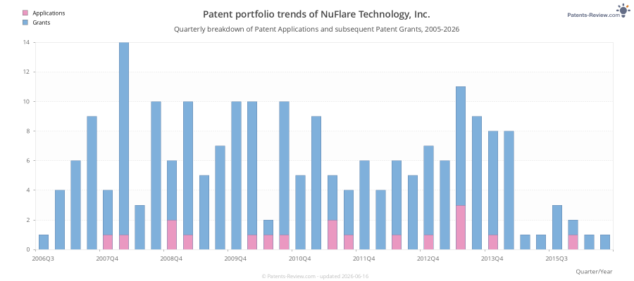
2017-03-09
195
2021-01-05
Top Inventors for applications by NuFlare Technology, Inc.
These are the the leading inventors for applications assigned to NuFlare Technology, Inc.:
- Takayuki Abe 32 Kanagawa, Japan
- Jun Yashima 22 Kanagawa, Japan
- Akihito Anpo 17 Tokyo, Japan
- Shuichi TAMAMUSHI 16 Kanagawa, Japan
- Hideo Tsuchiya 14 Tokyo, Japan
- NuFlare Technology, Inc. 11 Numazu-shi, Japan
- Hitoshi Higurashi 11 Kanagawa, Japan
- Shigehiro HARA 10 Kanagawa, Japan
- Tomohiro Iijima 9 Shizuoka, Japan
- Rieko NISHIMURA 9 Kanagawa, Japan
- Munehiro Ogasawara 8 Kanagawa, Japan
- Junichi Suzuki 8 Saitama, Japan
- Takanao TOUYA 8 Kanagawa, Japan
- Yasuo Kato 8 Kanagawa, Japan
- Hitoshi SUNAOSHI 7 Kanagawa, Japan
- Takashi KAMIKUBO 7 Tokyo, Japan
- Keiko EMI 7 Ibaraki, Japan
- Hiroshi MATSUMOTO 7 Shizuoka, Japan
- Noriaki NAKAYAMADA 7 Kanagawa, Japan
- Kiyoshi Hattori 6 Tokyo, Japan
- Seiji Wake 6 Shizuoka, Japan
- Riki OGAWA 6 Kanagawa, Japan
- Shusuke Yoshitake 6 Kanagawa, Japan
- Takafumi INOUE 6 Kanagawa, Japan
- Ryoichi Yoshikawa 5 Kanagawa, Japan
- Tomoyuki Horiuchi 5 Shizuoka, Japan
- Nobutaka Kikuiri 5 Tokyo, Japan
- Hideo Inoue 5 Kanagawa, Japan
- Makoto Hiramoto 4 Tokyo, Japan
- Yuusuke Sato 4 Tokyo, Japan
- Ikunao Isomura 4 Kanagawa, Japan
- Kunihiko Suzuki 4 Shizuoka, Japan
- Hirohito ANZE 4 Shizuoka, Japan
- Shinji SAKAMOTO 4 Kanagawa, Japan
- Hironobu MATSUMOTO 4 Kanagawa, Japan
- Jun Kasahara 4 Kanagawa, Japan
- Kenji OHTOSHI 4 Kanagawa, Japan
- Hidekazu Takekoshi 4 Kanagawa, Japan
- Junichi SUZUKI 4 Shizuoka, Japan
- Takashi Kamikubo 4 Kanagawa, Japan
- Takuya Matsukawa 3 Shizuoka, Japan
- NuFlare Technology, Inc. 3 , United States
- Yoshikuni GOSHIMA 3 Shizuoka, Japan
- Seiichi TSUCHIYA 3 Shizuoka, Japan
- Yujin HANDA 3 Shizuoka, Japan
- Tomoo Motosugi 3 Shizuoka, Japan
- Hayato Kimura 3 Shizuoka, Japan
- Osamu IIZUKA 3 Kanagawa, Japan
- Hiromu Inoue 3 Kanagawa, Japan
- Takeshi KUROHORI 3 Shizuoka, Japan
- Michihiro KAWAGUCHI 3 Shizuoka, Japan
- Hideki Ito 2 Shizuoka, Japan
- Hideyuki Tsurumaki 2 Kanagawa, Japan
- Kiminobu AKENO 2 Kanagawa, Japan
- Yoshiyuki MATSUNO 2 Shizuoka, Japan
- Yoshiro Yamanaka 2 Shizuoka, Japan
- Takayuki OHNISHI 2 Numazu-shi, Japan
- Susumu Oogi 2 Kanagawa, Japan
- Hironobu Hirata 2 Mishima, Japan
- Shuichi Tamamushi 2 Fujisawa-shi, Japan
- Kentaro OKUDA 2 Kanagawa, Japan
- Rieko Nishimura 2 Yokohama-shi, Japan
- Rieko Nishimura 2 Yokohama, Japan
- Shunji SHINKAWA 2 Shizuoka, Japan
- Hironobu HIRATA 2 Mishima-shi, Japan
- Kenji OHTOSHI 2 Kawasaki, Japan
- Takahito NAKAYAMA 2 Shizuoka, Japan
- Riki OGAWA 2 Kawasaki-shi, Japan
- Takehiko Katsumata 2 Shizuoka, Japan
- Hiroyuki Tanizaki 2 Mie, Japan
- Hideo INOUE 2 Mishima-shi, Japan
- Hiroshi Tsukada 2 Kanagawa, Japan
- Hiroyuki Ikeda 2 Kanagawa, Japan
- Eiji Matsumoto 2 Kanagawa, Japan
- Fumio Ozaki 2 Kanagawa, Japan
- Yuichi TACHIKAWA 2 Shizuoka, Japan
- Eiji Sawa 2 Kanagawa, Japan
- Hidenori SATO 2 Kanagawa, Japan
- Takeshi FUJIWARA 2 Kanagawa, Japan
- Kazuhiro SHIBA 2 Shizuoka, Japan
- Isaho KAMATA 2 Tokyo, Japan
- Takahito Nakayama 2 Kanagawa, Japan
- Keisuke YAMAGUCHI 2 Shizuoka, Japan
- Takumi Yamada 2 Shizuoka, Japan
- Takayuki OHNISHI 2 Shizuoka, Japan
- Shuichi Tamamushi 2 Fujisawa, Japan
- Yusuke Sakai 2 Kanagawa, Japan
- Masayoshi Yajima 2 Kanagawa-ken, Japan
- Masatoshi HIRONO 2 Yokohama-shi, Japan
- Kaoru TSURUTA 2 Kanagawa, Japan
- Takayuki Ohnishi 2 Numazu, Japan
- Kenji OHTOSHI 2 Kawasaki-shi, Japan
- Masanori Sugino 1 Kanagawa, Japan
- Hayato Kimura 1 Numazu, Japan
- Toshiro YAMAMOTO 1 Kanagawa, Japan
- Atsushi Hayamizu 1 Shizuoka, Japan
- Naohisa IKEYA 1 Kanagawa, Japan
- Tomohiro Iijima 1 Numazu-shi, Japan
- Tomohiro NAKAMURA 1 Tochigi, Japan
- Riki Ogawa 1 Kawasaki, Japan
Recent patent applications by NuFlare Technology, Inc.
NuFlare Technology, Inc. based in Numazu-shi, JP has been assigned the rights to these inventions. The list includes both Pending Applications and Patent Grants:
US20170068172A1
PhysicsMethod for fabricating semiconductor device, pattern writing apparatus, recording medium recording program, and pattern transfer apparatus
#2 | 2016-06-09 ✅ Patent 10,120,284 granted on 2018-11-06US20160161849A1
PhysicsMulti charged particle beam writing apparatus and multi charged particle beam writing method
#3 | 2015-12-31US20150377800A1
PhysicsPATTERN TEST APPARATUS
#4 | 2015-10-29 ✅ Patent 9,535,327 granted on 2017-01-03US20150309412A1
PhysicsMethod for fabricating semiconductor device, pattern writing apparatus, recording medium recording program, and pattern transfer apparatus
#5 | 2015-08-20 ✅ Patent 9,543,119 granted on 2017-01-10US20150235807A1
ElectricityMulti charged particle beam writing apparatus and method for correcting a current distribution of groups of charged particle beams
#6 | 2015-08-13 ✅ Patent 9,552,983 granted on 2017-01-24US20150228477A1
ElectricityManufacturing method for semiconductor device
#7 | 2015-07-09 ✅ Patent 9,406,117 granted on 2016-08-02US20150193918A1
PhysicsInspection system and method for inspecting line width and/or positional errors of a pattern
#8 | 2015-05-14 ✅ Patent 9,177,372 granted on 2015-11-03US20150131892A1
PhysicsDefect estimation device and method and inspection system and method
#9 | 2014-08-14 ✅ Patent 9,076,564 granted on 2015-07-07US20140225008A1
ElectricityMulti charged particle beam writing apparatus and multi charged particle beam writing method
#10 | 2014-03-20 ✅ Patent 9,018,602 granted on 2015-04-28US20140077103A1
ElectricityCharged particle beam writing apparatus and charged particle beam writing method
#11 | 2014-03-13 ✅ Patent 9,086,388 granted on 2015-07-21US20140072202A1
PhysicsPattern evaluation method and apparatus
#12 | 2014-03-06 ✅ Patent 9,343,266 granted on 2016-05-17US20140061499A1
ElectricityCharged particle beam pattern writing method and charged particle beam writing apparatus that corrects beam rotation utilizing a correlation table
#13 | 2014-02-27 ✅ Patent 9,157,870 granted on 2015-10-13US20140055780A1
PhysicsPattern test apparatus
#14 | 2014-02-27 ✅ Patent 9,194,817 granted on 2015-11-24US20140055774A1
PhysicsDefect detection method
#15 | 2014-02-27 ✅ Patent 8,803,108 granted on 2014-08-12US20140054469A1
ElectricityMethod for acquiring settling time
#16 | 2014-01-16 ✅ Patent 9,141,750 granted on 2015-09-22US20140017349A1
PhysicsCharged particle beam writing apparatus and irradiation time apportionment method of charged particle beams for multiple writing
#17 | 2014-01-02 ✅ Patent 8,742,376 granted on 2014-06-03US20140001380A1
ElectricityMethod and apparatus of mask drawing using a grounding body at lowest resistance value position of the mask
#18 | 2013-12-19 ✅ Patent 8,835,881 granted on 2014-09-16US20130334442A1
ElectricityDrift correction method and pattern writing data generation method
#19 | 2013-12-05 ✅ Patent 8,729,507 granted on 2014-05-20US20130320230A1
ElectricityMulti charged particle beam writing method and multi charged particle beam writing apparatus
#20 | 2013-11-28 ✅ Patent 9,268,234 granted on 2016-02-23US20130316288A1
PhysicsCharged particle beam lithography apparatus and charged particle beam pattern writing method
#21 | 2013-10-10 ✅ Patent 8,779,379 granted on 2014-07-15US20130264499A1
ElectricityAcquisition method of charged particle beam deflection shape error and charged particle beam writing method
#22 | 2013-10-10 ✅ Patent 9,164,044 granted on 2015-10-20US20130264478A1
PhysicsCharged particle beam lithography apparatus, inspection apparatus and inspection method of pattern writing data
#23 | 2013-10-03US20130256555A1
ElectricitySHAPING OFFSET ADJUSTMENT METHOD AND CHARGED PARTICLE BEAM DRAWING APPARATUS
#24 | 2013-10-03 ✅ Patent 8,872,141 granted on 2014-10-28US20130256519A1
ElectricityCharged particle beam writing apparatus and charged particle beam writing method
#25 | 2013-10-03 ✅ Patent 9,735,003 granted on 2017-08-15US20130255569A1
ElectricityFilm-forming apparatus and film-forming method
#26 | 2013-09-26 ✅ Patent 9,159,555 granted on 2015-10-13US20130253688A1
ElectricityMulti charged particle beam writing apparatus and multi charged particle beam writing method
#27 | 2013-09-26 ✅ Patent 9,082,588 granted on 2015-07-14US20130252172A1
ElectricityMulti charged particle beam writing apparatus and multi charged particle beam writing method
#28 | 2013-09-26 ✅ Patent 9,299,533 granted on 2016-03-29US20130252145A1
ElectricityMulti charged particle beam writing apparatus utilizing multiple staged mutually orthogonal beam blankers
#29 | 2013-09-26 ✅ Patent 9,235,883 granted on 2016-01-12US20130250095A1
PhysicsInspection system and method
#30 | 2013-09-19 ✅ Patent 8,927,941 granted on 2015-01-06US20130240750A1
ElectricityMulti charged particle beam writing apparatus and multi charged particle beam writing method with fixed voltage ratio einzel lens
#31 | 2013-08-22 ✅ Patent 9,373,424 granted on 2016-06-21US20130216953A1
PhysicsElectron beam writing apparatus and electron beam writing method
#32 | 2013-08-22 ✅ Patent 8,861,832 granted on 2014-10-14US20130216120A1
PhysicsInspection system and method
#33 | 2013-08-22 ✅ Patent 8,816,276 granted on 2014-08-26US20130214172A1
ElectricityElectron beam writing apparatus and electron beam writing method
#34 | 2013-07-11 ✅ Patent 8,767,200 granted on 2014-07-01US20130176559A1
PhysicsLuminous flux branching element and mask defect inspection apparatus
#35 | 2013-06-20 ✅ Patent 8,741,547 granted on 2014-06-03US20130157198A1
PhysicsMulti charged particle beam writing apparatus and multi charged particle beam writing method
#36 | 2013-06-20US20130156950A1
Chemistry; metallurgyFILM-FORMING APPARATUS AND FILM-FORMING METHOD
#37 | 2013-06-20US20130152853A1
Chemistry; metallurgyFILM-FORMING APPARATUS AND FILM-FORMING METHOD
#38 | 2013-05-30 ✅ Patent 8,759,799 granted on 2014-06-24US20130134329A1
ElectricityCharged particle beam writing apparatus and charged particle beam writing method
#39 | 2013-05-02US20130104800A1
Chemistry; metallurgyFILM-FORMING METHOD AND FILM-FORMING APPARATUS
#40 | 2013-04-25 ✅ Patent 8,552,405 granted on 2013-10-08US20130099139A1
ElectricityCharged particle beam writing apparatus and charged particle beam writing method
#41 | 2013-04-18 ✅ Patent 8,781,212 granted on 2014-07-15US20130094752A1
PhysicsDefect estimation device and method and inspection system and method
#42 | 2013-04-18 ✅ Patent 8,983,113 granted on 2015-03-17US20130093878A1
PhysicsDefect estimation device and method and inspection system and method
#43 | 2013-04-04 ✅ Patent 8,797,525 granted on 2014-08-05US20130083318A1
PhysicsPattern inspection apparatus and pattern inspection method
#44 | 2013-04-04 ✅ Patent 8,847,178 granted on 2014-09-30US20130082193A1
PhysicsCharged particle beam writing apparatus and charged particle beam writing method
#45 | 2013-04-04 ✅ Patent 8,492,732 granted on 2013-07-23US20130082187A1
ElectricityMulti charged particle beam writing apparatus and multi charged particle beam writing method
#46 | 2013-03-14 ✅ Patent 8,748,064 granted on 2014-06-10US20130065184A1
PhysicsCharged particle beam drawing method and charged particle beam drawing apparatus
#47 | 2013-03-07 ✅ Patent 8,710,467 granted on 2014-04-29US20130056647A1
ElectricityMulti charged particle beam writing apparatus and multi charged particle beam writing method
#48 | 2013-03-07 ✅ Patent 8,586,951 granted on 2013-11-19US20130056645A1
ElectricityMulti charged particle beam writing apparatus and multi charged particle beam writing method
#49 | 2013-02-21 ✅ Patent 9,542,586 granted on 2017-01-10US20130044205A1
PhysicsPattern inspection apparatus and pattern inspection method
#50 | 2013-02-14 ✅ Patent 8,748,843 granted on 2014-06-10US20130037724A1
ElectricityCharged particle beam drawing apparatus and charged particle beam drawing method
#51 | 2013-01-10 ✅ Patent 8,452,074 granted on 2013-05-28US20130010291A1
PhysicsApparatus and method for pattern inspection
#52 | 2012-12-27 ✅ Patent 9,273,412 granted on 2016-03-01US20120325138A1
Chemistry; metallurgyFilm-forming apparatus and film-forming method
#53 | 2012-12-06 ✅ Patent 10,578,560 granted on 2020-03-03US20120307043A1
PhysicsInspection apparatus and method for detecting false defects
#54 | 2012-11-22 ✅ Patent 8,563,952 granted on 2013-10-22US20120292537A1
ElectricityCharged particle beam writing apparatus
#55 | 2012-11-22 ✅ Patent 9,006,691 granted on 2015-04-14US20120292536A1
ElectricityCharged particle beam writing apparatus and charged particle beam writing method using a generated frame that surrounds a first data processing block
#56 | 2012-11-15US20120286174A1
ElectricityCHARGED PARTICLE BEAM WRITING APPARATUS AND CHARGED PARTICLE BEAM WRITING METHOD
#57 | 2012-10-04 ✅ Patent 9,122,176 granted on 2015-09-01US20120252215A1
PhysicsMethod for fabricating semiconductor device, pattern writing apparatus, recording medium recording program, and pattern transfer apparatus
#58 | 2012-10-04 ✅ Patent 8,779,394 granted on 2014-07-15US20120248340A1
ElectricityCharged particle beam writing apparatus and charged particle beam writing method
#59 | 2012-08-23 ✅ Patent 8,859,997 granted on 2014-10-14US20120211676A1
ElectricityCharged particle beam writing apparatus and charged particle beam writing method
#60 | 2012-08-23 ✅ Patent 9,063,440 granted on 2015-06-23US20120211674A1
ElectricityCharged particle beam writing apparatus and charged particle beam writing method
#61 | 2012-08-02 ✅ Patent 8,610,096 granted on 2013-12-17US20120193553A1
ElectricityCharged particle beam writing apparatus and method
#62 | 2012-07-26 ✅ Patent 8,755,040 granted on 2014-06-17US20120189032A1
PhysicsIlluminating apparatus, pattern inspection apparatus, and method of forming illuminating light
#63 | 2012-07-26 ✅ Patent 8,431,908 granted on 2013-04-30US20120187307A1
ElectricityCharged particle beam writing apparatus and charged particle beam writing method
#64 | 2012-06-07 ✅ Patent 9,057,711 granted on 2015-06-16US20120140060A1
PhysicsInspection apparatus and method
#65 | 2012-05-24 ✅ Patent 8,878,149 granted on 2014-11-04US20120126145A1
ElectricityCharged particle beam writing apparatus and charged particle beam writing method
#66 | 2012-05-03 ✅ Patent 8,352,889 granted on 2013-01-08US20120108063A1
ElectricityBeam dose computing method and writing method and record carrier body and writing apparatus
#67 | 2012-05-03 ✅ Patent 8,527,913 granted on 2013-09-03US20120104286A1
ElectricityMethod for resizing pattern to be written by lithography technique, and charged particle beam writing method
#68 | 2012-04-12 ✅ Patent 9,218,942 granted on 2015-12-22US20120085940A1
ElectricityCharged particle beam writing apparatus and charged particle beam writing method
#69 | 2012-04-05US20120081538A1
PhysicsPATTERN INSPECTION APPARATUS
#70 | 2012-03-22 ✅ Patent 8,563,953 granted on 2013-10-22US20120068089A1
ElectricityCharged particle beam writing apparatus and charged particle beam writing method
#71 | 2012-02-09 ✅ Patent 8,429,575 granted on 2013-04-23US20120036486A1
ElectricityMethod for resizing pattern to be written by lithography technique, and charged particle beam writing method
#72 | 2012-01-12 ✅ Patent 8,502,175 granted on 2013-08-06US20120007002A1
ElectricityCharged particle beam pattern forming apparatus and charged particle beam pattern forming method
#73 | 2012-01-05 ✅ Patent 8,466,440 granted on 2013-06-18US20120001097A1
ElectricityCharged particle beam drawing apparatus and control method thereof
#74 | 2011-12-01 ✅ Patent 9,188,853 granted on 2015-11-17US20110291029A1
PhysicsCharged particle beam drawing apparatus and control method thereof
#75 | 2011-11-24 ✅ Patent 8,301,291 granted on 2012-10-30US20110286319A1
ElectricityCharged particle beam writing apparatus, write data creation method and charged particle beam writing method
#76 | 2011-10-20 ✅ Patent 9,036,896 granted on 2015-05-19US20110255770A1
PhysicsInspection system and method for inspecting line width and/or positional errors of a pattern
#77 | 2011-10-20 ✅ Patent 8,427,919 granted on 2013-04-23US20110255388A1
ElectricityPattern writing system and method and abnormality diagnosing method
#78 | 2011-10-20 ✅ Patent 8,791,432 granted on 2014-07-29US20110253912A1
ElectricityCharged particle beam writing apparatus and charged particle beam writing method
#79 | 2011-10-20 ✅ Patent 8,610,091 granted on 2013-12-17US20110253911A1
PhysicsCharged particle beam writing apparatus and charged particle beam writing method
#80 | 2011-09-22 ✅ Patent 9,552,963 granted on 2017-01-24US20110231134A1
ElectricityCharged particle beam writing apparatus and method therefor
#81 | 2011-08-04 ✅ Patent 8,737,676 granted on 2014-05-27US20110188734A1
PhysicsDefect estimation device and method and inspection system and method
#82 | 2011-08-04US20110186744A1
ElectricityCHARGED PARTICLE BEAM APPARATUS AND METHOD
#83 | 2011-07-21 ✅ Patent 8,548,223 granted on 2013-10-01US20110176719A1
PhysicsInspection system and method
#84 | 2011-06-30 ✅ Patent 8,779,397 granted on 2014-07-15US20110155930A1
ElectricitySubstrate cover and charged particle beam writing method using same
#85 | 2011-05-26US20110121208A1
ElectricityCHARGED PARTICLE BEAM DRAWING APPARATUS AND ELECTRICAL CHARGING EFFECT CORRECTION METHOD THEREOF
#86 | 2011-05-19 ✅ Patent 8,653,488 granted on 2014-02-18US20110114853A1
PhysicsElectron beam apparatus
#87 | 2011-04-21 ✅ Patent 8,755,599 granted on 2014-06-17US20110091099A1
PhysicsReview apparatus and inspection system
#88 | 2011-04-21US20110089346A1
Performing operations; transportingMETHOD AND SYSTEM FOR PATTERN WRITING WITH CHARGED-PARTICLE BEAM
#89 | 2011-03-24 ✅ Patent 8,207,514 granted on 2012-06-26US20110068281A1
ElectricityCharged particle beam drawing apparatus and proximity effect correction method thereof
#90 | 2011-03-17 ✅ Patent 8,755,924 granted on 2014-06-17US20110066272A1
ElectricityCharged particle beam writing method and apparatus therefor
#91 | 2011-03-17 ✅ Patent 8,471,225 granted on 2013-06-25US20110066271A1
ElectricityCharged particle beam writing method and apparatus therefor
#92 | 2011-02-24 ✅ Patent 8,183,545 granted on 2012-05-22US20110046762A1
ElectricityCharged particle beam writing apparatus, charged particle beam writing method and apparatus of processing data for charged particle beam writing
#93 | 2011-02-24 ✅ Patent 8,903,158 granted on 2014-12-02US20110044529A1
PhysicsInspection system and inspection method
#94 | 2011-02-24 ✅ Patent 9,031,313 granted on 2015-05-12US20110044528A1
PhysicsInspection system
#95 | 2011-02-10 ✅ Patent 8,481,964 granted on 2013-07-09US20110033788A1
ElectricityCharged particle beam drawing apparatus and method
#96 | 2011-02-10 ✅ Patent 8,178,856 granted on 2012-05-15US20110031387A1
ElectricityCharged particle beam writing apparatus and method thereof
#97 | 2011-01-20 ✅ Patent 8,188,449 granted on 2012-05-29US20110012031A1
ElectricityCharged particle beam drawing method and apparatus
#98 | 2010-12-02 ✅ Patent 8,307,314 granted on 2012-11-06US20100306721A1
ElectricityWrite error verification method of writing apparatus and creation apparatus of write error verification data for writing apparatus
#99 | 2010-11-18 ✅ Patent 8,237,139 granted on 2012-08-07US20100290023A1
PhysicsMethod for detecting substrate position of charged particle beam photolithography apparatus and charged particle beam photolithography apparatus
#100 | 2010-11-18 ✅ Patent 8,247,783 granted on 2012-08-21US20100288939A1
ElectricityMethod of determining main deflection settling time for charged particle beam writing, method of writing with charged particle beam, and apparatus for writing with charged particle beam
Also check out NuFlare Technology, Inc.'s (Numazu-shi, Japan) applicant profile with 18 patent applications submitted.
3105 ⎘