Printed circuit boards having improved solder pads
US20050282415A1
2005-12-22
11/027,215
2004-12-29
✅ Patent granted
US 7,079,399 B2
2006-07-18
-
-
Javaid H. Nasri
2024-12-29
Abstract:
A printed circuit board having improved solder pads for preventing from short circuit of the printed circuit board caused by axial leads (30, 31) of components engaging the circuit surrounding the soldering pad comprises a pair of through holes (10, 11), a pair of first pads (20, 21) surrounding corresponding through holes and a pair of second pads (40, 41) adjacent corresponding first pads. When components are inserted into the through holes of the printed circuit board using placement machines, bent portions of the axial leads that are extended out of the first pads will fall into the second pads.
Assignee:
- HON HAI PRECISION INDUSTRY CO., LTD. 12,833 🇹🇼 Tu-Cheng, Taiwan
- HON HAI Precision Industry CO., LTD. 1,310 🇹🇼 Tu-Cheng City, Taiwan
Interested in similar patents?
Get notified when new applications in this technology area are published.
Classification:
H05K3/3447 » CPC main
Apparatus or processes for manufacturing printed circuits; Assembling printed circuits with electric components, e.g. with resistor electrically connecting electric components or wires to printed circuits by soldering Lead-in-hole components
H05K3/3447 » CPC main
Apparatus or processes for manufacturing printed circuits; Assembling printed circuits with electric components, e.g. with resistor electrically connecting electric components or wires to printed circuits by soldering Lead-in-hole components
H05K1/116 » CPC further
Printed circuits; Details; Printed elements for providing electric connections to or between printed circuits; Via connections; Lands around holes or via connections Lands, clearance holes or other lay-out details concerning the surrounding of a via
H05K1/116 » CPC further
Printed circuits; Details; Printed elements for providing electric connections to or between printed circuits; Via connections; Lands around holes or via connections Lands, clearance holes or other lay-out details concerning the surrounding of a via
H05K2201/0949 » CPC further
Indexing scheme relating to printed circuits covered by; Shape and layout; Shape and layout details of conductors; Pads and lands Pad close to a hole, not surrounding the hole
H05K2201/0949 » CPC further
Indexing scheme relating to printed circuits covered by; Shape and layout; Shape and layout details of conductors; Pads and lands Pad close to a hole, not surrounding the hole
H05K2201/09781 » CPC further
Indexing scheme relating to printed circuits covered by; Shape and layout; Shape and layout details of conductors covering at least two types of conductors provided for in - Dummy conductors, i.e. not used for normal transport of current; Dummy electrodes of components
H05K2201/09781 » CPC further
Indexing scheme relating to printed circuits covered by; Shape and layout; Shape and layout details of conductors covering at least two types of conductors provided for in - Dummy conductors, i.e. not used for normal transport of current; Dummy electrodes of components
H05K2201/10651 » CPC further
Indexing scheme relating to printed circuits covered by; Details of components or other objects attached to or integrated in a printed circuit board; Details of electrical connections of non-printed components, e.g. special leads; Components characterised by their electrical contacts Component having two leads, e.g. resistor, capacitor
H05K2203/1446 » CPC further
Indexing scheme relating to apparatus or processes for manufacturing printed circuits covered by; Related to the order of processing steps Treatment after insertion of lead into hole, e.g. bending, cutting, caulking or curing of adhesive but excluding soldering
H05K2203/1446 » CPC further
Indexing scheme relating to apparatus or processes for manufacturing printed circuits covered by; Related to the order of processing steps Treatment after insertion of lead into hole, e.g. bending, cutting, caulking or curing of adhesive but excluding soldering
H05K7/06 IPC
Constructional details common to different types of electric apparatus; Arrangements of circuit components or wiring on supporting structure on insulating boards, e.g. wiring harnesses
H05K7/06 IPC
Constructional details common to different types of electric apparatus; Arrangements of circuit components or wiring on supporting structure on insulating boards, e.g. wiring harnesses
Description
BACKGROUND OF THE INVENTION1. Field of the Invention
The present invention relates to a printed circuit board, and particularly to a printed circuit board which has improved solder pads layout.
2. Description of Related Art
Conventional printed circuit boards each define a plurality of through holes. The through holes are provided for extension of leads of components. The components are connected with the printed circuit board with the leads soldered thereto. A solder pad area is provided around each through hole when layout. Circuit is not laid in the pad areas and the pad areas are commonly covered with solder. The components are attached to the printed circuit board by wave soldering or reflow soldering. The pad areas are for preventing short circuit between the components and the circuit around the components on the printed circuit board.
Bigger components with axial leads are typically inserted into the printed circuit board manually. This insertion process is unduly laborious and time-consuming and has a low efficiency. An improved method of inserting components to corresponding through holes of the printed circuit board by placement machines is provided. This operation can greatly increase the efficiency.
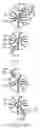
The axial leads of the components should be perpendicular to the printed circuit board. But the axial leads are often bent when the components are inserted into the through holes by machine. The bent angles are different according to different placement machine. FIGS. 5 to 8 show four kinds of commonly bent angles respectively. Through holes 10′ and 11′ of the printed circuit board provide a component (not shown) with two axial leads to extend therethrough. The through holes 10′ and 11′ are surrounded by solder pads 20′ and 21′, respectively. Numbers 30′ and 31′ indicate two axial leads of the components. Letters a1, a2, b1 and b2 respectively indicate the angles of that the axial lead 30′ and the axial lead 21′ away from the through hole 10′ and through hole 11′. The placement machine determines the values of a1, a2, b1 and b2. Usually, a1=a2=45 degrees, b1=b2=45 degrees. Commonly, only one of these bent angles will happen when one kind of placement machine is used to insert the components. When the axial lead of the component is out of the area of the soldering pad, it is prone to touch the circuit that surrounds the soldering pad. Thus a short circuit in the printed circuit board occurs and this causes damage to the printed circuit board.
An improved printed circuit board that overcomes the above-mentioned problems is desired.
SUMMARY OF THE INVENTIONAn object of the present invention is to provide a printed circuit board that has improved solder pad layout for preventing short circuit of the printed circuit board.
In order to achieve the above object, a printed circuit board having improved solder pads in accordance with a preferred embodiment of the present invention for preventing from short circuit of the printed circuit board caused by axial leads of components engaging the circuit surrounding the soldering pad comprises a pair of through holes, a pair of first pads surrounding corresponding through holes and a pair of second pads adjacent corresponding first pads. When components are inserted into the through holes of the printed circuit board using placement machines, bent portions of the axial leads that are extended out of the first pads will fall into the second pads.
Other objects, advantages and novel features of the present invention will become more apparent from the following detailed description when taken in conjunction with the accompanying drawings, in which:
BRIEF DESCRIPTION OF THE DRAWINGSFIGS. 1 to 4 are schematic views of four kinds of solder pads in accordance with a preferred embodiment of the present invention; and
FIGS. 5 to 8 are schematic views of four kinds of bending cases when using conventional solder pads.
DESCRIPTION OF THE INVENTIONFIGS. 1 to 4 illustrate a pair of solder pads in accordance with the present invention. A pair of plated through holes 10, 12 which may be arranged in a row is provided to receive conventional components such as a resistor which has axial leads 30, 31 formed therefrom to project through holes 10, 12. The components are electrically and physically connected to the printed circuit board by passing the entire printed circuit board through a wave soldering operation. A pair of first pads 20, 21 are located on a same surface of the printed circuit board and respectively around the through holes 10, 11. The first pads 20, 21 are covered with solder. A pair of second pads 40, 41 are circular and covered with the same solder of the first pads 20, 21. A plurality solder pads such as the first pads 20, 21 and the second pads 40, 41 are disposed on the printed circuit board. The solder pads have no circuits disposed thereon and are for preventing from short circuit between neighboring circuits. The second pad 40 and the first pad 20 are two tangent circles. The second pad 41 and the first pad 21 are two tangent circles.
The improvement point of this invention is to add the second pads 40, 41 around the first pads 20, 21. When the components are inserted into the printed circuit board using a placement machine, the bent portions of the axial leads 30, 31 that are extended out of the areas of the first pads 20, 21 can fall into the area of the second pads 40, 41. Therefore, the axial leads 30, 31 are prevented from engaging the circuit around the first pads 20, 21 thereby avoiding short circuit of the printed circuit board.
Commonly, only one kind of bent angle will happen when one kind of placement machine is used to insert the components. FIGS. 1 to 4 show four kinds of layouts of second pads 40, 41 according to the four kinds of commonly bent angles of the axial leads 30, 31. Referring to FIGS. 1 and 2, the axial leads 30, 31 are bent away from area of the first pads 20, 21. Bent angles c1, c2 or d1, d2 are formed between the axial leads 30, 31 and a connecting line between centers of the two through holes 10, 11. The bent angles c1, c2 or d1, d2 have certain values according to a same kind of placement machine. Usually, c1=c2=45 degrees, d1=d2=45 degrees. Referring to FIGS. 3 and 4, the axial leads 30, 31 are bent away or towards the area of the first pads 20, 21 along the connecting line between centers of the two through holes 10, 11. So when layout, a connecting line between a center of the second pad 40 and the center of the through hole 10 and a connecting line between a center of the disk 41 and the center of the through hole 11 should be in alignment with the bending directions of the axial leads 30, 31, respectively. A length of a diameter of the second pads 40, 41 can be counted according to the following formula:
d≧e−r
Wherein d is the diameter of the second 40 or 41, e is equal to a length of the axial leads 30, 31 minus a thickness of the printed circuit board, and r is a radius of the pad 20 or 21.
While a preferred embodiment in accordance with the present invention have been shown and described, equivalent modifications and changes known to persons skilled in the art according to the spirit of the present invention are considered within the scope of the present invention as defined in the appended claims.
Claims
1. A printed circuit board having improved solder pads for preventing from short circuit of the printed circuit board caused by axial leads of components engaging the circuit surrounding the soldering pad, comprising:
a pair of though holes for inserting of components;
a pair of first circular pads surrounding corresponding through holes; and
a pair of second circular pads, the first circular pads and the second circular pads are tangent to each other.
2. The printed circuit board as described in claim 1, wherein the first circular pads and the second circular pads are both not laid circuit thereon.
3. The printed circuit board as described in claim 1, wherein an angle between a line connecting a center of one of the first circular pads and a center of the corresponding second circular pad and a line connecting centers of the first circular pads is same to the bent angle of the axial leads of the components.
4. The printed circuit board as described in claim 3, wherein the diameter of the second circular pads is equal to a length of the axial leads minus a thickness of the printed circuit board and a radius of the pad.
5. The printed circuit board as described in claim 1, wherein the printed circuit board is a single-layer board.
6. The printed circuit board as described in claim 1, wherein the printed circuit board is a multi-layer board.
7. A printed circuit board having improved solder pads for preventing from short circuit of the printed circuit board caused by axial leads of components engaging the circuit surrounding the soldering pad, comprising:
a pair of though holes;
a pair of first pads surrounding corresponding through holes; and
a pair of second pads located adjacent corresponding first pads;
wherein when components are inserted into the through holes of the printed circuit board, bent portions of the axial leads that are extended out of the first pads will fall into areas of the second pads.
8. The printed circuit board as described in claim 7, wherein the first pads and the second pads are both not laid circuit thereon.
9. The printed circuit board as described in claim 7, wherein the first pads are circular.
10. The printed circuit board as described in claim 9, wherein the second pads are circular.
11. The printed circuit board as described in claim 10, wherein the first pads and the second pads are tangent to each other.
12. The printed circuit board as described in claim 11, wherein an angle between a line connecting a center of one of the first pads and a center of the corresponding second pad and a line connecting centers of the first pads is same to the bent angle of the axial leads of the components.
13. The printed circuit board as described in claim 12, wherein the diameter of the second pads is equal to a length of the axial leads minus a thickness of the printed circuit board and a radius of the pad.
14. The printed circuit board as described in claim 7, wherein the printed circuit board is a single-layer board.
15. The printed circuit board as described in claim 7, wherein the printed circuit board is a multi-layer board.
16. A method for solderable attachment of an electrically conductive lead of a component to a circuit board, comprising the steps of:
placing said lead on said circuit board;
providing a solderable first pad on said circuit board corresponding to said lead along an extending direction of said lead; and
forming a solderable second pad on said circuit board independent from said first pad to allow placement and soldering of said lead on said circuit board via said first and second pads exclusively.
17. The method as described in claim 16, wherein said first and second pads are formed tangent to each other.
18. The method as described in claim 16, further comprising the step of placing said lead in a through hole formed in said circuit board and extending from a center of said first pad.
Images & Drawings included:


Sources:
- United States Patent and Trademark Office - verify current appl. status at the USPTO↗
Similar patent applications:
Recent applications in this class:
- » 20220377909 2022-11-24
Electronic-component carrier board and a wiring method for the same - » 20210410293 2021-12-30
Method for producing a connection contact - » 20210329791 2021-10-21
Printed circuit board and manufacturing method thereof, and electronic device - » 20210315106 2021-10-07
MICROSWITCH BASED POSITION SENSOR WITH HARNESS RELIEF FOR MOTORIZED VALVE - » 20210307179 2021-09-30
Multi-core cable assembling method and multi-core cable assembly producing method - » 20190254174 2019-08-15
Component mounting method, component mounting system, and manufacturing method of component mounting board - » 20190116675 2019-04-18
MOUNTING DEVICE ON A CIRCUIT BOARD AND METHOD FOR MOUNTING AN OBJECT ON A CIRCUIT BOARD - » 20180343748 2018-11-29
Substrate on which electronic component is soldered, electronic device, method for soldering electronic component - » 20180192523 2018-07-05
Back-drilled through-hole printed circuit board (PCB) systems - » 20170142845 2017-05-18
Increasing solder hole-fill in a printed circuit board assembly
Recent applications for this Assignee:
- » 20140363586 2014-12-11
Laser-based method for growing an array of carbon nanotubes - » 20140299819 2014-10-09
Method for making a carbon nanotube film - » 20140233961 2014-08-21
Optical communication module including optical-electrical signal converters and optical signal generators - » 20140199855 2014-07-17
Method for making a carbon nanotube film - » 20140083669 2014-03-27
HEAT SINK - » 20140063746 2014-03-06
Electronic device with heat dissipation assembly - » 20140061224 2014-03-06
AUTOMATIC VENDING MACHINE - » 20140060914 2014-03-06
Enclosure with shield apparatus - » 20140058727 2014-02-27
MULTIMEDIA RECORDING SYSTEM AND METHOD - » 20140055955 2014-02-27
Fastener