Substrate design to improve chip package reliability
US20060103006A1
2006-05-18
10/988,100
2004-11-12
✅ Patent granted
US 7,105,920 B2
2006-09-12
-
-
Andy Huynh
2024-11-12
Abstract:
A substrate design to improve chip package reliability is provided. The chip package includes a substrate having a ceramic layer formed in a recess. A die is attached to the substrate on the ceramic layer. The substrate may be attached to a printed circuit board. The substrate may be fabricated by forming a recess in a substrate, such as a multi-layer substrate formed of organic dielectric materials. A ceramic layer is then affixed to the substrate in the recess. A die may be attached to the ceramic layer and the substrate may be attached to a printed circuit board.
Inventors:
- Pei-Haw Tsao 63 🇹🇼 Tai-Chung, Taiwan
- Chuen-Jye Lin 11 🇹🇼 Taichung, Taiwan
- Chao-Yuan Su 7 🇹🇼 Koahsiung City, Taiwan
- Chao-Yuan Su 12 🇹🇼 Koahsiung, Taiwan
- Chen-Der Huang 2 🇹🇼 Hsin-Chu, Taiwan
- Chuen-Jye Lin 1 🇹🇼 Taichung City, Taiwan
Assignee:
- TAIWAN SEMICONDUCTOR MANUFACTURING COMPANY, LTD. 8,890 🇹🇼 Hsin-Chu, Taiwan
Interested in similar patents?
Get notified when new applications in this technology area are published.
Classification:
H05K1/0271 » CPC main
Printed circuits; Details Arrangements for reducing stress or warp in rigid printed circuit boards, e.g. caused by loads, vibrations or differences in thermal expansion
H05K1/0271 » CPC main
Printed circuits; Details Arrangements for reducing stress or warp in rigid printed circuit boards, e.g. caused by loads, vibrations or differences in thermal expansion
H01L23/13 » CPC further
Details of semiconductor or other solid state devices; Mountings, e.g. non-detachable insulating substrates characterised by the shape
H01L23/49833 » CPC further
Details of semiconductor or other solid state devices; Arrangements for conducting electric current to or from the solid state body in operation, e.g. leads, terminal arrangements ; Selection of materials therefor consisting of soldered constructions; Leads, on insulating substrates, the chip support structure consisting of a plurality of insulating substrates
H01L23/145 » CPC further
Details of semiconductor or other solid state devices; Mountings, e.g. non-detachable insulating substrates characterised by the material or its electrical properties Organic substrates, e.g. plastic
H01L23/15 » CPC further
Details of semiconductor or other solid state devices; Mountings, e.g. non-detachable insulating substrates characterised by the material or its electrical properties Ceramic or glass substrates
H01L2224/16 » CPC further
Indexing scheme for arrangements for connecting or disconnecting semiconductor or solid-state bodies and methods related thereto as covered by; Means for bonding being attached to, or being formed on, the surface to be connected, e.g. chip-to-package, die-attach, "first-level" interconnects; Manufacturing methods related thereto; Bump connectors; Manufacturing methods related thereto; Structure, shape, material or disposition of the bump connectors after the connecting process of an individual bump connector
H01L2924/01322 » CPC further
Indexing scheme for arrangements or methods for connecting or disconnecting semiconductor or solid-state bodies as covered by; Alloys; Binary Alloys Eutectic Alloys, i.e. obtained by a liquid transforming into two solid phases
H01L2924/15311 » CPC further
Indexing scheme for arrangements or methods for connecting or disconnecting semiconductor or solid-state bodies as covered by; Details of package parts other than the semiconductor or other solid state devices to be connected; Die mounting substrate; Connection portion the connection portion being formed only on the surface of the substrate opposite to the die mounting surface being a ball array, e.g. BGA
H05K2201/0187 » CPC further
Indexing scheme relating to printed circuits covered by; Dielectrics; Dielectric layers with regions of different dielectrics in the same layer, e.g. in a printed capacitor for locally changing the dielectric properties
H05K2201/0187 » CPC further
Indexing scheme relating to printed circuits covered by; Dielectrics; Dielectric layers with regions of different dielectrics in the same layer, e.g. in a printed capacitor for locally changing the dielectric properties
H05K2201/068 » CPC further
Indexing scheme relating to printed circuits covered by; Thermal details wherein the coefficient of thermal expansion is important
H05K2201/068 » CPC further
Indexing scheme relating to printed circuits covered by; Thermal details wherein the coefficient of thermal expansion is important
H05K2201/10674 » CPC further
Indexing scheme relating to printed circuits covered by; Details of components or other objects attached to or integrated in a printed circuit board; Details of electrical connections of non-printed components, e.g. special leads; Components characterised by their electrical contacts Flip chip
H01L2924/10253 » CPC further
Indexing scheme for arrangements or methods for connecting or disconnecting semiconductor or solid-state bodies as covered by; Details of semiconductor or other solid state devices to be connected; Material of the semiconductor or solid state bodies; Semiconducting materials; Elemental semiconductors, i.e. Group IV Silicon [Si]
H01L2924/00 » CPC further
Indexing scheme for arrangements or methods for connecting or disconnecting semiconductor or solid-state bodies as covered by
H01L2924/00014 » CPC further
Indexing scheme for arrangements or methods for connecting or disconnecting semiconductor or solid-state bodies as covered by; Technical content checked by a classifier the subject-matter covered by the group, the symbol of which is combined with the symbol of this group, being disclosed without further technical details
H01L2924/00011 » CPC further
Indexing scheme for arrangements or methods for connecting or disconnecting semiconductor or solid-state bodies as covered by; Technical content checked by a classifier Not relevant to the scope of the group, the symbol of which is combined with the symbol of this group
H01L2224/0401 » CPC further
Indexing scheme for arrangements for connecting or disconnecting semiconductor or solid-state bodies and methods related thereto as covered by; Means for bonding being attached to, or being formed on, the surface to be connected, e.g. chip-to-package, die-attach, "first-level" interconnects; Manufacturing methods related thereto; Bonding areas; Manufacturing methods related thereto; Structure, shape, material or disposition of the bonding areas prior to the connecting process Bonding areas specifically adapted for bump connectors, e.g. under bump metallisation [UBM]
H01L23/06 IPC
Details of semiconductor or other solid state devices; Containers; Seals characterised by the material of the container or its electrical properties
H01L23/12 IPC
Details of semiconductor or other solid state devices Mountings, e.g. non-detachable insulating substrates
Description
TECHNICAL FIELDThe present invention relates generally to semiconductor chip design and, more specifically, to flip chip packages.
BACKGROUNDGenerally, semiconductor chips used in electronic devices comprise a semiconductor die mounted on a carrier or a substrate. The semiconductor die is manufactured using standard semiconductor fabrication processes and has a series of bond pads that are used to make electrical contact to the integrated circuit formed therein. The die is placed on a carrier or substrate that has electrical leads formed therein to correspond to the bond pads of the die. Solder balls are typically used to attached the die to the substrate. The die and the carrier may be enclosed to protect the die from the environment.
The die and the substrate to which the die is mounted, however, frequently exhibit different coefficients of thermal expansion. For example, dies are commonly fabricated from silicon, which has a coefficient of thermal expansion between about 2.8 and 3.0. On the other hand, the substrates, typically made of organic dielectric materials and metal lines, have a coefficient of thermal expansion between 17.0 and 20.0. Thus, as the die and substrate are heated and cooled through normal use, the substrate expands and contracts at a much greater rate than the die. This difference in the expansion and contraction may induce serious sheer stress at the joint between the substrate and the die during temperature cycling, thereby causing the bump joints to crack. This is particularly true for high lead bumps.
One attempt at mitigating this effect involved eliminating the use of solder bumps. Rather, the substrate layers are built directly upon the die. These attempts, however, may adversely affect the yield of the die. In particular the yield of the die is tied to the yield of the substrate. Thus, if the substrate fails for any reason, the die must also be discarded.
Thus, what is needed is a method of attaching a die to a substrate to achieve a connection point that is less susceptible to the stress resulting from differing coefficients of thermal expansion.
SUMMARY OF THE INVENTIONThese and other problems are generally solved or circumvented, and technical advantages are generally achieved, by embodiments of the present invention, which provides a chip package that reduces shear stress between a substrate and a die.
In an embodiment of the present invention, a chip package is provided. The chip package comprises a substrate having a ceramic die mount attached thereto. A die is then attached to the ceramic die mount.
In another embodiment of the present invention, a method of forming a chip package is provided. Specifically, a built-up substrate including a die-mount area is provided. An ceramic layer is attached to the substrate within the die-mount area. A die is mounted onto the exposed ceramic layer.
The foregoing has outlined rather broadly the features and technical advantages of the present invention in order that the detailed description of the invention that follows may be better understood. Additional features and advantages of the invention will be described hereinafter which form the subject of the claims of the invention. It should be appreciated by those skilled in the art that the conception and specific embodiment disclosed may be readily utilized as a basis for modifying or designing other structures or processes for carrying out the same purposes of the present invention. It should also be realized by those skilled in the art that such equivalent constructions do not depart from the spirit and scope of the invention as set forth in the appended claims.
BRIEF DESCRIPTION OF THE DRAWINGSFor a more complete understanding of the present invention, and the advantages thereof, reference is now made to the following descriptions taken in conjunction with the accompanying drawing, in which:
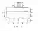
FIG. 1 schematically illustrates an embodiment of the present invention.
DETAILED DESCRIPTION OF ILLUSTRATIVE EMBODIMENTSThe making and using of the presently preferred embodiments are discussed in detail below. It should be appreciated, however, that the present invention provides many applicable inventive concepts that can be embodied in a wide variety of specific contexts. The specific embodiments discussed are merely illustrative of specific ways to make and use the invention, and do not limit the scope of the invention.
Generally, embodiments of the present invention involve embedding a ceramic layer into a substrate, wherein a die is subsequently mounted to the ceramic layer. The ceramic layer serves to minimize the coefficient of thermal expansion mismatch between the die and the substrate.
Referring now to FIG. 1, a portion of a packaged die is shown. The packaged die includes a substrate 22 mounted to a printed circuit board (PCB) 32 via solder bumps 34, the substrate having a die 18 mounted thereto via solder bumps 20. In an embodiment, the substrate 22 may be a multi-layer substrate, commonly referred to as a built-up substrate, comprising multiple organic dielectric layers and metal lines/vias formed therein.
For example, in an embodiment the substrate 22 includes a core layer 10 positioned between a lower sub-substrate 12 and an upper sub-substrate 14. The core layer 10 is preferably not a halogen free layer having a glass transition point (Tg) of about 185° C. as measured by a dynamic mechanical analysis (DMA) and having a Young's modulus of about 26 GPa. The core layer 10 may have a water absorption of about 0.1%. In this embodiment, the lower sub-substrate 12 and the upper sub-substrate 14 may comprise a halogen free film having a glass transition point (Tg) of about 183° C. as measured by a DMA and having a Young's modulus of about 2.4 GPa. The lower sub-substrate 12 and the upper sub-substrate 14 may exhibit a tensile strength of about 89 MPa and an elongation of about 14%. The lower sub-substrate 12 and the upper sub-substrate 14 may have a water absorption of about 1.4%.
It should be noted that the substrate discussed above is only an example of a substrate that may be used with an embodiment of the present invention. Other substrates may be used.
It should also be noted that each of the layers described above may comprise multiple layers. Furthermore, metallization lines (not shown) may be formed therein to route electrical contacts of the die 18 to specific metal contacts on the bottom of the substrate 22 (located at the solder bumps 34).
As shown in FIG. 1, a ceramic layer 16 is mounted to the substrate 22 where the die 18 is to be attached to the substrate 22. In a preferred embodiment, the ceramic layer 16 is laminated to a recessed portion of the substrate 22, preferably such that a surface of the ceramic layer 16 and the substrate 22 are coplanar. By embedding/laminating ceramic layer 16 in the substrate 22, the difference between the coefficient of thermal expansion between adjacent materials is reduced. Reducing the coefficient of thermal expansion between adjacent materials has been found to eliminate or reduce the cracking of the solder bumps due to the shear strain caused by the difference in the coefficient of thermal expansion.
For example, a die 18 may have a coefficient of thermal expansion between about 2.8 and about 3.0, and the ceramic layer 16 may have a coefficient of thermal expansion between about 3.0 to 4.0. Thus, the difference between the coefficient of thermal expansion of the die 18 and the ceramic material is less than the difference between the coefficient of thermal expansion of the substrate 22, which typically has a coefficient of thermal expansion between 17.0 to 20.0.
Solder bumps 20 and 34 are preferably comprised of eutectic lead as it has a lower melting temperature than high-lead.
Thus, advantages of embodiments of the present invention include the coefficient of thermal expansion mismatch between the build up layer and the silicon die is minimized while the coefficient of thermal expansion match is maintained with the PCB board.
The scope of the present application is not intended to be limited to the particular embodiments of the process, machine, manufacture, composition of matter, means, methods and steps described in the specification. As one of ordinary skill in the art will readily appreciate from the disclosure of the present invention, processes, machines, manufacture, compositions of matter, means, methods, or steps, presently existing or later to be developed, that perform substantially the same function or achieve substantially the same result as the corresponding embodiments described herein may be utilized according to the present invention. Accordingly, the appended claims are intended to include within their scope such processes, machines, manufacture, compositions of matter, means, methods, or steps.
Claims
What is claimed is:1. A method of forming a chip package, comprising the steps of:
providing a substrate having a recess;
positioning a ceramic layer in the recess; and
mounting a die onto the ceramic layer.
2. The method of claim 1, wherein the positioning the ceramic layer includes laminating the ceramic layer in the recess.
3. The method of claim 1, wherein the substrate comprises a built-up substrate having a core positioned between a lower built-up sub-substrate and an upper built-up sub-substrate.
4. The method of claim 1, wherein a surface of the ceramic layer and a surface of the substrate are substantially coplanar.
5. The method of claim 1, wherein the mounting a die is performed by using solder bumps positioned between the die and the ceramic layer.
6. The method of claim 5, wherein the solder bumps comprise eutectic lead bumps.
7. The method of claim 1, wherein the die has a coefficient of thermal expansion from about 2.8 to about 3.0 and the ceramic layer has a coefficient of thermal expansion from about 3.0 to about 4.0.
8. The method of claim 1, further including mounting the substrate to a printed-circuit board, the substrate being mounted to the printed-circuit board on a side opposite of the die.
9. The method of claim 8, wherein the mounting the substrate to a printed circuit-board is performed by using a series of solder bumps positioned between the substrate and the printed circuit board.
10. The method of claim 9, wherein the solder bumps comprise eutectic lead bumps.
11. A chip package comprising:
a substrate having a recess;
a ceramic layer mounted in the recess; and
a die mounted onto the ceramic layer.
12. The chip package of claim 11, wherein the ceramic layer is laminated to the substrate in the recess.
13. The chip package of claim 11, wherein the substrate includes a core positioned between a lower built-up sub-substrate and an upper built-up sub-substrate.
14. The chip package of claim 11, wherein a surface of the ceramic layer and a surface of the substrate are substantially coplanar.
15. The chip package of claim 11, wherein the die is mounted to the ceramic layer by solder bumps positioned between the die and the ceramic layer.
16. The chip package of claim 15, wherein the solder bumps comprise eutectic lead bumps.
17. The chip package of claim 11, wherein the die has a coefficient of thermal expansion from about 2.8 to about 3.0 and the ceramic layer has a coefficient of thermal expansion from about 3.0 to about 4.0.
18. The chip package of claim 11, further comprising a printed circuit board mounted to the substrate, the substrate being mounted to the printed-circuit board on a side opposite the die.
19. The chip package of claim 18, wherein the printed circuit board is mounted to the substrate by a series of solder bumps positioned between the substrate and the printed circuit board.
20. The chip package of claim 19, wherein the solder bumps comprise eutectic lead bumps.
Images & Drawings included:

Sources:
- United States Patent and Trademark Office - verify current appl. status at the USPTO↗
Recent applications in this class:
- » 20250254790 2025-08-07
GLASS CIRCUIT BOARD AND MANUFACTURING METHOD THEREOF AND IMAGING DEVICE - » 20250240877 2025-07-24
WIRING CIRCUIT BOARD - » 20250240876 2025-07-24
WIRING BOARD - » 20250240875 2025-07-24
LENS MODULE AND TERMINAL DEVICE - » 20250227838 2025-07-10
CAMERA MODULE AND VEHICLE CAMERA - » 20250212321 2025-06-26
SUBSTRATE AND MANUFACTURING METHOD THEREOF - » 20250212320 2025-06-26
METHOD FOR ACCOMMODATING SUBSTRATE WARPAGE IN PRINTED CIRCUIT BOARD ASSEMBLIES - » 20250203761 2025-06-19
CIRCUIT BOARD AND SEMICONDUCTOR PACKAGE COMPRISING SAME - » 20250194001 2025-06-12
PRINTED CIRCUIT BOARD - » 20250185158 2025-06-05
COPPER-CERAMIC BONDED SUBSTRATE AND METHOD FOR MANUFACTURING THE SAME
Recent applications for this Assignee:
- » 20240266341 2024-08-08
HYBRID BONDING WITH UNIFORM PATTERN DENSITY - » 20240224489 2024-07-04
SEMICONDUCTOR DEVICE - » 20240170063 2024-05-23
CONTENT ADDRESSABLE MEMORY ARRAY DEVICE STRUCTURE - » 20240161819 2024-05-16
MEMORY DEVICE AND MANUFACTURING THEREOF - » 20240153896 2024-05-09
SEMICONDUCTOR PACKAGE SYSTEM AND METHOD - » 20240120409 2024-04-11
Method for non-resist nanolithography - » 20240113080 2024-04-04
Semiconductor Device with Discrete Blocks - » 20240105632 2024-03-28
Method for forming a semiconductor device including forming a first interconnect structure on one side of a substrate having first metal feature closer the substrate than second metal feature and forming first and second tsv on other side of substrate connecting to the metal features - » 20240096816 2024-03-21
Method of manufacture overlay mark using laser marking process for semiconductor device - » 20240096383 2024-03-21
MEMORY DEVICE