Stacked memory card and method for manufacturing the same
US20060289980A1
2006-12-28
11/165,114
2005-06-22
Abstract:
A structure of stacked memory card, the structure includes a substrate, a lower chip, wires, adhered element, upper chip, and compound resin. The substrate has an upper surface formed with a plurality of first electrodes, and a lower surface. The B-stage glue is coated on the upper surface of the substrate. The lower chip is arranged on the upper surface of the substrate, and is located on the B-stage glue. The plurality of wires are electrically connected the lower chip to the first electrode of the substrate. The adhesive element includes adhesive agent and filling elements is coated on the lower chip. The upper chip is adhered on the lower chip by adhesive element, and is spaced with the lower chip through the filling element, then is electrically connected to the first electrode of the substrate by wires. The compound resin is encapsulated on the upper chip, lower chip, and wires.
Inventors:
- Hong Tsu Chang 4 🇹🇼 Hsinchu Hsien, Taiwan
- Dennis Pai 5 🇹🇼 Hsinchu Hsien, Taiwan
- Frank Lung 3 🇹🇼 Hsinchu Hsien, Taiwan
- Jay Lin 5 🇹🇼 Hsinchu Hsien, Taiwan
- Men San Lung 3 🇹🇼 Hsinchu Hsien, Taiwan
- Wilson Huang 1 🇹🇼 Hsinchu Hsien, Taiwan
Interested in similar patents?
Get notified when new applications in this technology area are published.
Classification:
H01L24/83 » CPC main
Arrangements for connecting or disconnecting semiconductor or solid-state bodies; Methods or apparatus related thereto; Methods for connecting semiconductor or other solid state bodies using means for bonding being attached to, or being formed on, the surface to be connected using a layer connector
H01L23/3121 » CPC further
Details of semiconductor or other solid state devices; Encapsulations, e.g. encapsulating layers, coatings, e.g. for protection characterised by the arrangement or shape the device being completely enclosed a substrate forming part of the encapsulation
H01L24/27 » CPC further
Arrangements for connecting or disconnecting semiconductor or solid-state bodies; Methods or apparatus related thereto; Means for bonding being attached to, or being formed on, the surface to be connected, e.g. chip-to-package, die-attach, "first-level" interconnects; Manufacturing methods related thereto; Layer connectors, e.g. plate connectors, solder or adhesive layers; Manufacturing methods related thereto Manufacturing methods
H01L24/29 » CPC further
Arrangements for connecting or disconnecting semiconductor or solid-state bodies; Methods or apparatus related thereto; Means for bonding being attached to, or being formed on, the surface to be connected, e.g. chip-to-package, die-attach, "first-level" interconnects; Manufacturing methods related thereto; Layer connectors, e.g. plate connectors, solder or adhesive layers; Manufacturing methods related thereto; Structure, shape, material or disposition of the layer connectors prior to the connecting process of an individual layer connector
H01L24/32 » CPC further
Arrangements for connecting or disconnecting semiconductor or solid-state bodies; Methods or apparatus related thereto; Means for bonding being attached to, or being formed on, the surface to be connected, e.g. chip-to-package, die-attach, "first-level" interconnects; Manufacturing methods related thereto; Layer connectors, e.g. plate connectors, solder or adhesive layers; Manufacturing methods related thereto; Structure, shape, material or disposition of the layer connectors after the connecting process of an individual layer connector
H01L25/0657 » CPC further
Assemblies consisting of a plurality of individual semiconductor or other solid state devices ; Multistep manufacturing processes thereof all the devices being of a type provided for in the same subgroup of groups - , e.g. assemblies of rectifier diodes the devices not having separate containers the devices being of a type provided for in group Stacked arrangements of devices
H01L23/5388 » CPC further
Details of semiconductor or other solid state devices; Arrangements for conducting electric current within the device in operation from one component to another, i.e. interconnections, e.g. wires, lead frames the interconnection structure between a plurality of semiconductor chips being formed on, or in, insulating substrates for flat cards, e.g. credit cards
H01L24/48 » CPC further
Arrangements for connecting or disconnecting semiconductor or solid-state bodies; Methods or apparatus related thereto; Means for bonding being attached to, or being formed on, the surface to be connected, e.g. chip-to-package, die-attach, "first-level" interconnects; Manufacturing methods related thereto; Wire connectors; Manufacturing methods related thereto; Structure, shape, material or disposition of the wire connectors after the connecting process of an individual wire connector
H01L24/73 » CPC further
Arrangements for connecting or disconnecting semiconductor or solid-state bodies; Methods or apparatus related thereto Means for bonding being of different types provided for in two or more of groups , , , , , , ,
H01L24/85 » CPC further
Arrangements for connecting or disconnecting semiconductor or solid-state bodies; Methods or apparatus related thereto; Methods for connecting semiconductor or other solid state bodies using means for bonding being attached to, or being formed on, the surface to be connected using a wire connector
H01L2224/83136 » CPC further
Indexing scheme for arrangements for connecting or disconnecting semiconductor or solid-state bodies and methods related thereto as covered by; Methods for connecting semiconductor or other solid state bodies using means for bonding being attached to, or being formed on, the surface to be connected using a layer connector; Aligning involving guiding structures, e.g. spacers or supporting members
H01L2224/83856 » CPC further
Indexing scheme for arrangements for connecting or disconnecting semiconductor or solid-state bodies and methods related thereto as covered by; Methods for connecting semiconductor or other solid state bodies using means for bonding being attached to, or being formed on, the surface to be connected using a layer connector; Bonding techniques using a polymer adhesive, e.g. an adhesive based on silicone, epoxy, polyimide, polyester; Hardening the adhesive by curing, i.e. thermosetting Pre-cured adhesive, i.e. B-stage adhesive
H01L2224/85 » CPC further
Indexing scheme for arrangements for connecting or disconnecting semiconductor or solid-state bodies and methods related thereto as covered by; Methods for connecting semiconductor or other solid state bodies using means for bonding being attached to, or being formed on, the surface to be connected using a wire connector
H01L2225/0651 » CPC further
Details relating to assemblies covered by the group but not provided for in its subgroups; All the devices being of a type provided for in the same subgroup of groups - the devices not having separate containers the devices being of a type provided for in group; Stacked arrangements of devices Wire or wire-like electrical connections from device to substrate
H01L2225/06575 » CPC further
Details relating to assemblies covered by the group but not provided for in its subgroups; All the devices being of a type provided for in the same subgroup of groups - the devices not having separate containers the devices being of a type provided for in group; Stacked arrangements of devices Auxiliary carrier between devices, the carrier having no electrical connection structure
H01L2924/01005 » CPC further
Indexing scheme for arrangements or methods for connecting or disconnecting semiconductor or solid-state bodies as covered by; Chemical elements Boron [B]
H01L2924/07802 » CPC further
Indexing scheme for arrangements or methods for connecting or disconnecting semiconductor or solid-state bodies as covered by; Polymers; Adhesive characteristics other than chemical not being an ohmic electrical conductor
H01L2224/83192 » CPC further
Indexing scheme for arrangements for connecting or disconnecting semiconductor or solid-state bodies and methods related thereto as covered by; Methods for connecting semiconductor or other solid state bodies using means for bonding being attached to, or being formed on, the surface to be connected using a layer connector; Arrangement of the layer connectors prior to mounting wherein the layer connectors are disposed only on another item or body to be connected to the semiconductor or solid-state body
H01L2924/181 » CPC further
Indexing scheme for arrangements or methods for connecting or disconnecting semiconductor or solid-state bodies as covered by; Details of package parts other than the semiconductor or other solid state devices to be connected Encapsulation
H01L2924/00012 » CPC further
Indexing scheme for arrangements or methods for connecting or disconnecting semiconductor or solid-state bodies as covered by; Technical content checked by a classifier Relevant to the scope of the group, the symbol of which is combined with the symbol of this group
H01L2224/45099 » CPC further
Indexing scheme for arrangements for connecting or disconnecting semiconductor or solid-state bodies and methods related thereto as covered by; Means for bonding being attached to, or being formed on, the surface to be connected, e.g. chip-to-package, die-attach, "first-level" interconnects; Manufacturing methods related thereto; Wire connectors; Manufacturing methods related thereto; Structure, shape, material or disposition of the wire connectors prior to the connecting process of an individual wire connector; Core members of the connector Material
H01L2924/00 » CPC further
Indexing scheme for arrangements or methods for connecting or disconnecting semiconductor or solid-state bodies as covered by
H01L2924/00014 » CPC further
Indexing scheme for arrangements or methods for connecting or disconnecting semiconductor or solid-state bodies as covered by; Technical content checked by a classifier the subject-matter covered by the group, the symbol of which is combined with the symbol of this group, being disclosed without further technical details
H01L2224/73265 » CPC further
Indexing scheme for arrangements for connecting or disconnecting semiconductor or solid-state bodies and methods related thereto as covered by; Means for bonding being of different types provided for in two or more of groups; Location after the connecting process on different surfaces Layer and wire connectors
H01L2924/207 » CPC further
Indexing scheme for arrangements or methods for connecting or disconnecting semiconductor or solid-state bodies as covered by; Parameters Diameter ranges
H01L23/02 IPC
Details of semiconductor or other solid state devices Containers; Seals
H01L21/00 IPC
Processes or apparatus adapted for the manufacture or treatment of semiconductor or solid state devices or of parts thereof
Description
BACKGROUND OF THE INVENTION1. Field of the Invention
The invention relates to a stacked memory card and method for manufacturing the same, and particular to memory card with B-stage glue for forming a stacked memory card, the reliability of the stacked memory card may be promoted.
2. Description of the Related Art
A conventional stacked memory card includes upper chip and lower chip, the upper chip is adhered on the lower chip by way of non-conductive glue, and the lower chip is adhered on the substrate by the non-conductor glue, while the quality of the non-conductor glue is property, the lower chip is bumpy, so that the stacked memory card is bumpy.
SUMMARY OF THE INVENTIONAn objective of the invention is to provide a stacked memory card and a method for manufacturing the same capable of increasing the reliability of the stacked memory card.
To achieve the above-mentioned object, the invention includes a substrate, B-stage glue, lower chip, wires, an adhesive element, an upper chip, and a compound resin. The substrate has an upper surface formed with a plurality of first electrodes, and a lower surface. The B-stage glue is coated on the upper surface of the substrate. The lower chip is arranged on the upper surface of the substrate, and is located on the B-stage glue. The wires are electrically connected the lower chip to the first electrode of the substrate. The adhesive element includes an adhesive agent and filling elements coated on the lower chip. The upper chip is adhered on the lower chip by adhesive element, and spaced with the lower chip through the filling element, then is electrically connected to the first electrode of the substrate by wires. The compound resin encapsulated on the upper chip, lower chip, and wires.
BRIEF DESCRIPTION OF THE DRAWINGSFIG. 1 is a cross-sectional view schematic illustration showing a stacked memory card of the present invention.
FIG. 2 is a first illustration showing a method for manufacturing a stacked memory card of the present invention.
FIG. 3 is a second illustration showing a method for manufacturing a stacked memory card of the present invention.
FIG. 4 is a third illustration showing a method for manufacturing a stacked memory card of the present.
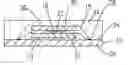
DETAILED DESCRIPTION OF THE INVENTIONPlease refer to FIG. 1 is a stacked memory card of the present invention includes a substrate 10, B-stage glue 12, lower chip 14, wires 16, an adhesive element 18, an upper chip 20, and a compound resin 22.
The substrate 10 has an upper surface 24 formed with a plurality of first electrodes 28, and a lower surface 26.
The B-stage glue 12 is coated on the upper surface 24 of the substrate 10 by printing matter.
The lower chip 14 is arranged on the upper surface 24 of the substrate 10, and is located on the B-stage glue 12.
The wires 16 are electrically connected the lower chip 14 to the first electrode 18 of the substrate 10.
The adhesive element 16 coated on the lower chip 14 includes an adhesive agent 30 and filling elements 32, in the embodiment, the filling elements 32 are ball sharp.
The upper chip 20 is adhered on the lower chip 14 by adhesive element 16, and is spaced with the lower chip 14 through the filling element 32, then is electrically connected to the first electrode 28 of the substrate 10 by wires 16.
The compound resin 22 is encapsulated on the upper chip 20, lower chip 14, and wires 16.
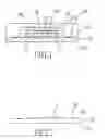
Please refer to FIG. 2 is a first illustration showing a method for manufacturing a stacked memory card of the present invention. Firstly, providing a substrate 10 having an upper surface 24 formed with a plurality of first electrodes 28, and a lower surface 26.
Providing B-stage glue 12 coated on the upper surface 24 of the substrate 10 by printing matter. Then, first curing the B-stage 12 coated on the substrate
Please refer to FIG. 3 is a second illustration showing a method for manufacturing a stacked memory card of the present invention. Providing a lower chip 14 arranged on the upper surface 24 of the substrate 10, and located on the B-stage glue 12, curing the B-stage 12 coated on the substrate 10, thus, the lower chip 14 is mounted on the substrate 10.
Providing wires 16 electrically connected the lower chip 14 to the first electrode 18 of the substrate 10.
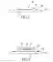
Please refer to FIG. 4 is a second illustration showing a method for manufacturing a stacked memory card of the present invention. Providing adhesive element 16 coated on the lower chip 14 has an adhesive agent 30 and filling elements 32, in the embodiment, the filling elements 32 are ball sharp.
Providing an upper chip 20 adhered on the lower chip 14 by adhesive element 16, and spaced with the lower chip 14 through the filling element 32, then is electrically connected to the first electrode 28 of the substrate 10 by wires 16.
Finally, providing a compound resin 22 encapsulated on the upper chip 20, lower chip 14, and wires 16.
While the invention has been described by the way of an example and in terms of a preferred embodiment, it is to be understood that the invention is not limited to the disclosed embodiment. On the contrary, it is intended to cover various modifications. Therefore, the scope of the appended claims should be accorded the broadest interpretation so as to encompass all such modifications.
Claims
1. A structure of stacked memory card, comprising;
a substrate having an upper surface formed with a plurality of first electrodes, and a lower surface;
a B-stage glue coated on the upper surface of the substrate;
a lower chip arranged on the upper surface of the substrate, and located on the B-stage glue;
a plurality of wires electrically connected the lower chip to the first electrode of the substrate;
a adhesive element including adhesive agent and filling elements coated on the lower chip;
an upper chip adhered on the lower chip by adhesive element, and spaced with the lower chip through the filling element, then electrically connected to the first electrode of the substrate by wires; and
a compound resin encapsulated on the upper chip, lower chip, and wires.
2. (canceled)
3. (canceled)
4. A method for manufacturing a substrate of memory card, the method comprising the step of;
Providing a substrate having an upper surface formed with a plurality of first electrodes, and a lower surface;
Providing a B-stage glue coated on the upper surface of the substrate, and first curing the B-stage glue;
Providing a lower chip arranged on the upper surface of the substrate, and located on the B-stage glue, and second curing the B-stage glue, so as to the lower chip fixed on the substrate;
Providing a plurality of wires electrically connected the lower chip to the first electrode of the substrate;
Providing a adhesive element including adhesive agent and filling elements coated on the lower chip;
Providing an upper chip adhered on the lower chip by adhesive element, and spaced with the lower chip through the filling element, then electrically connected to the first electrode of the substrate by wires; and
Providing a compound resin encapsulated on the upper chip, lower chip, and wires.
5. The structure of stacked memory card according to claim 1, wherein the B-stage glue is coated on the lower chip by printing way.
6. The structure of stacked memory card according to claim 1, wherein the filling elements are balls.
Images & Drawings included:
Sources:
- United States Patent and Trademark Office - verify current appl. status at the USPTO↗
Similar patent applications:
Recent applications in this class:
- » 20250167170 2025-05-22
LASER TRANSFER OF MICROELECTRONIC DEVICE AND ASSOCIATED CONDUCTIVE PAD - » 20250140738 2025-05-01
SEMICONDUCTOR MANUFACTURING APPARATUS, METHOD OF MANUFACTURING SEMICONDUCTOR APPARATUS, AND SEMICONDUCTOR APPARATUS - » 20250132288 2025-04-24
PROCESS FOR FLIP CHIP PACKAGING - » 20250125304 2025-04-17
METHOD OF MANUFACTURING A CHIP STRUCTURE AND CHIP STRUCTURE - » 20250087628 2025-03-13
METHOD OF SURFACE MODIFICATION FOR WAFER BONDING - » 20250079395 2025-03-06
METHOD OF MANUFACTURING SEMICONDUCTOR PACKAGE - » 20250070080 2025-02-27
METHOD OF BONDING CHIPS AND A SYSTEM FOR PERFORMING THE METHOD - » 20250062276 2025-02-20
METHOD FOR DIPPING ADHESIVE MATERIAL - » 20250046751 2025-02-06
CONTROLLING ADHESIVE REFLOW FOR TRANSFER PRINTING - » 20250022842 2025-01-16
SEMICONDUCTOR PACKAGE