Method for manufacturing substrate with cavity
US20070066045A1
2007-03-22
11/524,404
2006-09-21
✅ Patent granted
US 7,498,205 B2
2009-03-03
-
-
Alexander G Ghyka | Seahvosh J Nikmanesh
2027-05-15
Abstract:
A method for manufacturing a substrate having a cavity is disclosed. The method comprises: (a) forming a barrier around a predetermined area where the cavity is to be formed on a copper foil laminated master, an internal circuit formed in the copper foil laminated master; (b) coating a thermosetting material in the area where the cavity is to be formed; (c) laminating a dielectric layer and a copper foil layer on the copper foil laminated master, on which the thermosetting material is coated; (d) pressing the laminated dielectric layer and copper foil layer using a press plate, on which a protruded part is formed in an area corresponding to the area where the cavity is to be formed; (e) forming an external circuit pattern in the upper part of the laminated dielectric layer; and (f) dissolving the coated thermosetting material using a solvent and forming the cavity. The method in accordance with the present invention can mount a plurality of integrated circuits by reducing the thickness of a substrate on a package on package.
Inventors:
- Jung-Hyun Park 29 🇰🇷 Daejeon, South Korea
- Myung-Sam Kang 37 🇰🇷 Daejeon, South Korea
- Hoe-Ku Jung 20 🇰🇷 Daejeon, South Korea
Assignee:
- SAMSUNG ELECTRO-MECHANICS CO., LTD. 3,010 🇰🇷 Suwon, South Korea
- SAMSUNG ELECTRO-MECHANICS CO., LTD. 5,757 🇰🇷 Suwon-si, South Korea
Interested in similar patents?
Get notified when new applications in this technology area are published.
Classification:
H01L21/00 IPC
Processes or apparatus adapted for the manufacture or treatment of semiconductor or solid state devices or of parts thereof
H01L2224/73265 » CPC further
Indexing scheme for arrangements for connecting or disconnecting semiconductor or solid-state bodies and methods related thereto as covered by; Means for bonding being of different types provided for in two or more of groups; Location after the connecting process on different surfaces Layer and wire connectors
H05K3/4652 » CPC main
Apparatus or processes for manufacturing printed circuits; Manufacturing multilayer circuits by building the multilayer layer by layer, i.e. build-up multilayer circuits Adding a circuit layer by laminating a metal foil or a preformed metal foil pattern
H05K3/4652 » CPC main
Apparatus or processes for manufacturing printed circuits; Manufacturing multilayer circuits by building the multilayer layer by layer, i.e. build-up multilayer circuits Adding a circuit layer by laminating a metal foil or a preformed metal foil pattern
H01L21/481 » CPC further
Processes or apparatus adapted for the manufacture or treatment of semiconductor or solid state devices or of parts thereof; Manufacture or treatment of semiconductor devices or of parts thereof the devices having at least one potential-jump barrier or surface barrier, e.g. PN junction, depletion layer or carrier concentration layer; Manufacture or treatment of parts, e.g. containers, prior to assembly of the devices, using processes not provided for in a single one of the subgroups -; Insulating or insulated parts, e.g. mountings, containers, diamond heatsinks Insulating layers on insulating parts, with or without metallisation
H05K3/4697 » CPC further
Apparatus or processes for manufacturing printed circuits; Manufacturing multilayer circuits having cavities, e.g. for mounting components
H05K3/4697 » CPC further
Apparatus or processes for manufacturing printed circuits; Manufacturing multilayer circuits having cavities, e.g. for mounting components
H01L23/13 » CPC further
Details of semiconductor or other solid state devices; Mountings, e.g. non-detachable insulating substrates characterised by the shape
H01L23/49805 » CPC further
Details of semiconductor or other solid state devices; Arrangements for conducting electric current to or from the solid state body in operation, e.g. leads, terminal arrangements ; Selection of materials therefor consisting of soldered constructions; Leads, on insulating substrates, the leads being also applied on the sidewalls or the bottom of the substrate, e.g. leadless packages for surface mounting
H01L24/73 » CPC further
Arrangements for connecting or disconnecting semiconductor or solid-state bodies; Methods or apparatus related thereto Means for bonding being of different types provided for in two or more of groups , , , , , , ,
H01L25/0657 » CPC further
Assemblies consisting of a plurality of individual semiconductor or other solid state devices ; Multistep manufacturing processes thereof all the devices being of a type provided for in the same subgroup of groups - , e.g. assemblies of rectifier diodes the devices not having separate containers the devices being of a type provided for in group Stacked arrangements of devices
H01L25/105 » CPC further
Assemblies consisting of a plurality of individual semiconductor or other solid state devices ; Multistep manufacturing processes thereof all the devices being of a type provided for in the same subgroup of groups - , e.g. assemblies of rectifier diodes the devices having separate containers the devices being of a type provided for in group
H01L2225/0651 » CPC further
Details relating to assemblies covered by the group but not provided for in its subgroups; All the devices being of a type provided for in the same subgroup of groups - the devices not having separate containers the devices being of a type provided for in group; Stacked arrangements of devices Wire or wire-like electrical connections from device to substrate
H01L2225/06568 » CPC further
Details relating to assemblies covered by the group but not provided for in its subgroups; All the devices being of a type provided for in the same subgroup of groups - the devices not having separate containers the devices being of a type provided for in group; Stacked arrangements of devices; Geometry of the stack, e.g. form of the devices, geometry to facilitate stacking the devices decreasing in size, e.g. pyramidical stack
H01L2924/01078 » CPC further
Indexing scheme for arrangements or methods for connecting or disconnecting semiconductor or solid-state bodies as covered by; Chemical elements Platinum [Pt]
H01L2924/01079 » CPC further
Indexing scheme for arrangements or methods for connecting or disconnecting semiconductor or solid-state bodies as covered by; Chemical elements Gold [Au]
H01L2924/15153 » CPC further
Indexing scheme for arrangements or methods for connecting or disconnecting semiconductor or solid-state bodies as covered by; Details of package parts other than the semiconductor or other solid state devices to be connected; Die mounting substrate; Shape the die mounting substrate comprising a recess for hosting the device
H01L2924/1517 » CPC further
Indexing scheme for arrangements or methods for connecting or disconnecting semiconductor or solid-state bodies as covered by; Details of package parts other than the semiconductor or other solid state devices to be connected; Die mounting substrate Multilayer substrate
H01L2924/15331 » CPC further
Indexing scheme for arrangements or methods for connecting or disconnecting semiconductor or solid-state bodies as covered by; Details of package parts other than the semiconductor or other solid state devices to be connected; Die mounting substrate; Connection portion the connection portion being formed on the die mounting surface of the substrate the connection portion being formed both on the die mounting surface of the substrate and outside the die mounting surface of the substrate being a ball array, e.g. BGA
H05K1/183 » CPC further
Printed circuits; Printed circuits structurally associated with non-printed electric components associated with components mounted in the printed circuit board, e.g. insert mounted components [IMC] Components mounted in and supported by recessed areas of the printed circuit board
H05K2203/0769 » CPC further
Indexing scheme relating to apparatus or processes for manufacturing printed circuits covered by; Treatments involving liquids, e.g. plating, rinsing; Uses of liquids, e.g. rinsing, coating, dissolving Dissolving insulating materials, e.g. coatings, not used for developing resist after exposure
H05K2203/308 » CPC further
Indexing scheme relating to apparatus or processes for manufacturing printed circuits covered by; Details of processes not otherwise provided for in - Sacrificial means, e.g. for temporarily filling a space for making a via or a cavity or for making rigid-flexible PCBs
H05K2203/308 » CPC further
Indexing scheme relating to apparatus or processes for manufacturing printed circuits covered by; Details of processes not otherwise provided for in - Sacrificial means, e.g. for temporarily filling a space for making a via or a cavity or for making rigid-flexible PCBs
H01L2924/00014 » CPC further
Indexing scheme for arrangements or methods for connecting or disconnecting semiconductor or solid-state bodies as covered by; Technical content checked by a classifier the subject-matter covered by the group, the symbol of which is combined with the symbol of this group, being disclosed without further technical details
H01L2924/15311 » CPC further
Indexing scheme for arrangements or methods for connecting or disconnecting semiconductor or solid-state bodies as covered by; Details of package parts other than the semiconductor or other solid state devices to be connected; Die mounting substrate; Connection portion the connection portion being formed only on the surface of the substrate opposite to the die mounting surface being a ball array, e.g. BGA
H01L2924/00012 » CPC further
Indexing scheme for arrangements or methods for connecting or disconnecting semiconductor or solid-state bodies as covered by; Technical content checked by a classifier Relevant to the scope of the group, the symbol of which is combined with the symbol of this group
H01L2924/14 » CPC further
Indexing scheme for arrangements or methods for connecting or disconnecting semiconductor or solid-state bodies as covered by; Details of semiconductor or other solid state devices to be connected; Device type Integrated circuits
H01L2924/00 » CPC further
Indexing scheme for arrangements or methods for connecting or disconnecting semiconductor or solid-state bodies as covered by
H01L21/44 IPC
Processes or apparatus adapted for the manufacture or treatment of semiconductor or solid state devices or of parts thereof; Manufacture or treatment of semiconductor devices or of parts thereof the devices having at least one potential-jump barrier or surface barrier, e.g. PN junction, depletion layer or carrier concentration layer the devices having semiconductor bodies not provided for in groups, , , and with or without impurities, e.g. doping materials Manufacture of electrodes on semiconductor bodies using processes or apparatus not provided for in groups -
Description
BACKGROUND OF THE INVENTION1. Field of the Invention
The present invention relates to a stacked-type semiconductor package module, more specifically to a method for manufacturing a substrate, on which a cavity is formed.
2. Description of the Related Art
With the development of the electronics industry, there has been increasing demands for electronic parts that perform better and are smaller. To accommodate these demands, the semiconductor packing technologies have been evolving from packing one integrated circuit on one substrate to packing several integrated circuits on one substrate. Moreover, to address the need for realizing high-performance, high-density packages, and to meet the demand for these packages, the “package on package (POP)” technology has been introduced. However, minimizing the thickness of the package has been a challenge to overcome for successful implementation of the POP technology.
FIG. 1 is a sectional view of a package on package in accordance with the prior art. FIG. 1 shows a lower package 110, an upper package 120, an upper solder ball 103, and a lower solder ball 140.
The conventional ball grid array (BGA) semiconductor package has a substrate body, in which a plurality of patterned conductive wires are installed. On top of the substrate body are a plurality of chip pads, to which semiconductor chips are wire-bonded. In addition, some area of the top of the substrate body is molded with an epoxy compound and forms a molding part, such that the semiconductor chip and metal wire are enveloped. Adhered to the bottom of the substrate are a plurality of solder balls such that the other ends of the conductive wires installed in the substrate can be connected. This structure of a conventional ball grip array semiconductor package is too thick to be stacked as a highly integrated memory module within a limited area.
The lower package 110 of the conventional package on package has a dual-level structure, and an integrated circuit is mounted on the surface of this substrate. The substrate of the lower package 100 is manufactured in the same method as manufacturing a general printed circuit board. The increasing density in the semiconductor package module necessitates the mounting of a plurality of integrated circuits. With the conventional method, it is difficult to increase the mounting in the lower package 110 while maintaining the overall height of the package on package. The die-thinning method, which reduces the thickness of a semiconductor chip, can be one way of reducing the height, but this raises the issue of function-error with a prolonged operation. Therefore, improvement in mounting capacity of the package on package is attempted by reducing the thickness of the substrate.
Since there are limitations to how thin the substrate can be made, the number of integrated circuits that can be mounted in the lower semiconductor package is also limited. Besides, embedding a semiconductor package in the substrate requires a drilling process, which is complicated and costly.
SUMMARY OF CERTAIN INVENTIVE ASPECTSThe present invention features a method for manufacturing a substrate with a cavity that manufactures a package on package substrate, on which a plurality of integrated circuits can be mounted by reducing the thickness of the substrate.
The present invention also provides a method for manufacturing a substrate with a cavity that can reduce the overall thickness of the semiconductor package by mounting the integrated circuits in the cavity.
The present invention also provides a method for manufacturing a substrate with a cavity that can simplify the process by mounting the integrated circuits in the cavity formed on the substrate, without using a separate drilling process.
Moreover, the present invention provides a method for manufacturing a substrate with a cavity that can make the package relatively thinner than other packages, on which the same number of integrated circuits are mounted, by incorporating the integrated circuits in the cavity formed on the substrate.
Furthermore, the present invention provides a method for manufacturing a substrate with a cavity that has a better finishing process than the conventional cavity-forming process by forming the cavity without using a separate drilling process.
The present invention also provides a method for manufacturing a substrate with a cavity that can mount multiple tiers of a plurality of integrated circuits in a lower package of a package on package.
Moreover, the present invention provides a method for manufacturing a substrate with a cavity that can reduce the thickness of a package on package substrate having at least 3 tiers.
In addition, the present invention provides a method for manufacturing a substrate with a cavity that can reduce the manufacturing cost by eliminating the need for an additional cavity-forming process.
An aspect of the present invention features a method for manufacturing a substrate, on which a cavity is formed. The method can comprise (a) forming a barrier around a predetermined area where the cavity is to be formed on a copper foil laminated master, an internal circuit formed in the copper foil laminated master; (b) coating a thermosetting material in the area where the cavity is to be formed; (c) laminating a dielectric layer and a copper foil layer on the copper foil laminated master, on which the thermosetting material is coated; (d) pressing the laminated dielectric layer and copper foil layer using a press plate, on which a protruded part is formed in an area corresponding to the area where the cavity is to be formed; (e) forming an external circuit pattern in the upper part of the laminated dielectric layer; and (f) dissolving the coated thermosetting material using a solvent and forming the cavity.
The dielectric layer and copper foil layer can be a resin coated copper foil, or the dielectric layer can be a prepreg.
The barrier can be printed by use of a screen method or by exposing a thermosetting film.
The glass transition temperature (Tg) of the thermosetting material can be higher than the glass transition temperature (Tg) of the dielectric layer.
The thermosetting material can be a material that does not mix with the dielectric layer.
The method can further comprise (g) depositing in the formed cavity a bonding pad for electrically connecting an element and the substrate, by use of electrolytic plating or electroless plating.
BRIEF DESCRIPTION OF THE DRAWINGSThese and other features, aspects, and advantages of the present invention will become better understood with regard to the following description, appended claims, and accompanying drawings where:
FIG. 1 shows a sectional view of a package on package in accordance with the prior art;
FIG. 2 shows a general illustration of a sectional view of a package on package in accordance with a preferred embodiment of the present invention;
FIG. 3 shows a sectional view of a package on package in accordance with a preferred embodiment of the present invention; and
FIGS. 4-11 illustrate the method for manufacturing a substrate, on which a cavity is formed, used for a package on package in accordance with a preferred embodiment of the present invention.
DETAILED DESCRIPTION OF CERTAIN INVENTIVE EMBODIMENTSHereinafter, preferred embodiments of the method for manufacturing a substrate with a cavity will be described in detail with reference to the accompanying drawings. In referencing the accompanying drawings, identical elements are given the same reference numerals, regardless of their figure numbers, and any redundant description thereof will be omitted. In addition, prior to describing preferred embodiments of the present invention, the method for manufacturing a general substrate will be described first. Although the method for manufacturing a multi-layer substrate is described, the present invention is by no means restricted to the method for manufacturing a multi-layer substrate.
First, an internal circuit pattern is formed on the outside of a core layer. An inner-layer base material that meets the product specification is cut, and a predetermined internal circuit pattern is formed using a dry film and a working film. Here, the inner layer can be scrubbed, and an inner layer dry film can be laminated, and the inner layer can be exposed/developed.
Then, prior to bonding the inner layer, on which the circuit pattern is formed, to the outer layer, a brown (black) oxide process is carried out in order to strengthen the adhesion. That is, the surface of a copper foil is chemically oxidized to enhance the surface roughness such that the lamination results in better adhesion. Then, by laminating the inner-layer substrate and a prepreg, prelamination and lamination processes are carried out.
Then, the laminated inner layer substrate and the prepreg are vacuum pressed. It is possible that the laminated inner layer substrate and the prepreg are hot pressed or cool pressed, instead of being vacuum pressed.
The resin and copper foil are trimmed from the corners of the panel, and an X-ray target drilling process, in which a hole is made at a target guide mark on the inner layer circuit, is carried out in preparation of a drilling process.
Then, the drilling process is carried out for electric conduction between the layers of the substrate. Here, a computer numerical control (CNC) method can be used for the drilling process.
Then, the outer layer is coated with the dry film and the working film in order to form a circuit pattern, exposed to a light of a predetermined intensity for a predetermined duration, and the unirradiated areas are developed in an etching process. After examining the outer layer and measuring the scale, a solder resist exposure film is designed and manufactured. Then, a preprocess, such as brush polishing, in which the surface of copper foil is made rough such that the solder resist ink is better adhered to the substrate, is carried out. The solder resist is then coated; the solder resist is exposed using the solder resist exposure film, designed adaptively in the preceding process; the solder resist is removed in a development process; and a variety of postprocesses, including electric/final tests, are carried out.
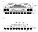
FIG. 2 is a general illustration of the cut section of a semiconductor package, constituting a package on package, in accordance with a preferred embodiment of the present invention. Referring to FIG. 2, the semiconductor package in accordance with the present invention comprises a core layer 210, a conductive circuit 220, a metal pad 230, an integrated circuit 240, a metal wire 250, a molding part 260, and a solder ball 270.
According to the present invention, at least one integrated circuit 240 is seated and located in a cavity, which is formed on a substrate, in order to reduce the thickness of the semiconductor package. That is, the cavity is formed in the upper part of the core layer 210 of a package on package, using a dielectric layer, and the integrated circuit 240 is inserted in the formed cavity. Then, the integrated circuit 240 is electrically coupled to the conductive circuit 220 and the metal pad 230, using the metal wire 250. Using a protective material, such as epoxy resin, the molding part is formed around and on top of the integrated circuit 240.
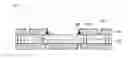
FIG. 3 is a sectional view of a package on package in accordance with a preferred embodiment of the present invention. Referring to FIG. 3, the substrate in accordance with the present invention can comprise a core layer 310, an internal circuit 320, a dielectric layer 330, an interstitial via hole (IVH) 335, an external circuit 340, a solder resist 350, a blind via hole (BVH) 355, a barrier 360, and a bonding pad 370.
The core layer 310 can be a copper foil laminated master, on which the internal circuit 320 is formed, and the dielectric layer 330 can be made of a dielectric material, such as a prepreg or a resin coated copper foil (RCC).
The internal circuit 320 and the external circuit 340 can be electrically connected to each other by the IVH 335 and the BVH 355. Here, the internal circuit 320 and the external circuit 340 can also be electrically connected to each other by a plated through hole (PTH, not shown).
The barrier 360 is for preventing the flow of a thermosetting material, which is prepared for forming the cavity. In case of a copper foil laminated master, in which an internal circuit is formed, the barrier can be a dielectric paste around an area, in which the cavity is to be formed.
The bonding pad 370 is seated in the cavity and connects a semiconductor chip and the substrate. The semiconductor chip and the substrate can be coupled to each other through flip-chip bonding or wire bonding.
FIGS. 4-11 illustrate the method for manufacturing the substrate, on which the cavity is formed, used for a package on package in accordance with a preferred embodiment of the present invention.
Referring to FIG. 4, the internal circuit 320 is formed on the copper foil laminated master 310. Here, processes such as exposure, developing, and etching are applied using an IVH, plating, and a dry film.
Referring to FIG. 5, the barrier 360 is formed around the area in which the cavity is to be formed. Here, the barrier 360 can be printed by using a screen method or exposing a thermosetting film. The barrier 360 blocks the flow between the thermosetting material, prepared for forming the cavity, and the dielectric layer 330. Hence, a high degree of precision is required for the barrier 360 since the boundary of the area in which the cavity is formed is defined by the barrier 360.
Referring to FIG. 6, the thermosetting material 610 is coated on the area in which the cavity is to be formed. The thermosetting material can be a liquid. An amount of the liquid thermosetting material that is sufficient to form the cavity is coated in the area surrounded by the barrier 360, and becomes solid in due time at room temperature. The thermosetting material can be a material that does not mix with the dielectric layer 330. If the thermosetting material does not mix with the dielectric layer 330, the thermosetting material becomes coated only in the area where the cavity is to be formed, resulting in a distinct cavity when the thermosetting material is etched.
Referring to FIG. 7, the upper and lower layers of the core layer (or the copper foil laminated master in which an internal circuit is printed) are laminated with a resin coated copper foil (RCC) 330 and 340 or a prepreg (PPG) 330 and a copper foil 340. Here, a prepreg or a bonding sheet can be used for laminating the dielectric layer on the core layer (or the copper foil laminated master in which an internal circuit is printed). The press plate (or a Sus plate) 710 and 720 has a protruded part, by which the cavity is formed when pressed. The shape of the protruded part, formed on the press plate 710, corresponds to the shape of the cavity to be formed. In other words, the protruded part formed on the press plate 710 fits the area surrounded by the barrier 360.
Referring to FIG. 8, the substrate is pressed by the press plate (or a Sus plate) 710 and 720 at a predetermined temperature. The material used for the substrate during the lamination has the following specifications: The liquid thermosetting material has a higher glass transition temperature (Tg) during the lamination than that of the dielectric material, and becomes a viscous liquid as the temperature rises. The dielectric material, which becomes more viscous than the liquid thermosetting material at a lower temperature, flows out of the protruded part during the lamination.
Referring to FIG. 9, the BVH 355 is formed using a laser drill after the lamination is completed, in order to couple the upper and lower layers electrically.
Referring to FIG. 10, the BVH 355 is plated, and a circuit pattern is formed on it. Here, the copper foil in the cavity is etched. Referring to FIG. 11, the thermosetting material, remaining in the cavity after forming the circuit, is dissolved by a solvent and removed, thereby forming the cavity. Then, a solder resist process is carried out, and the bonding pad 370 is formed through electroless plating or electrolytic plating to complete the substrate. The completed substrate with the cavity is the same substrate shown in FIG. 3.
As described above, the method in accordance with the present invention for manufacturing a substrate with a cavity can manufacture a package on package substrate, on which a plurality of integrated circuits can be mounted by reducing the thickness of the substrate.
The method for manufacturing a substrate with a cavity can reduce the overall thickness of the semiconductor package by mounting the integrated circuits in the cavity.
The method for manufacturing a substrate with a cavity can simplify the process by mounting the integrated circuits in the cavity formed on the substrate, without using a separate drilling process.
Moreover, the method for manufacturing a substrate with a cavity can make the package relatively thinner than other packages, on which the same number of integrated circuits are mounted, by incorporating the integrated circuits in the cavity formed on the substrate.
Furthermore, the present invention provides a method for manufacturing a substrate with a cavity that has a better finishing process than the conventional cavity-forming process by forming the cavity without using a separate drilling process.
The present invention also provides a method for manufacturing a substrate with a cavity that can mount multiple tiers of a plurality of integrated circuits in a lower package of a package on package.
Moreover, the present invention provides a method for manufacturing a substrate with a cavity that can reduce the thickness of a package on package substrate having at least 3 tiers.
In addition, the present invention provides a method for manufacturing a substrate with a cavity that can reduce the manufacturing cost by eliminating the need for an additional cavity-forming process.
Although a certain preferred embodiment of the present invention has been described, anyone of ordinary skill in the art to which the invention pertains should be able to understand that a large number of modifications and permutations are possible within the spirit and scope of the invention and its equivalents, which shall only be defined by the claims, appended below.
Claims
What is claimed is:1. A method for manufacturing a substrate, the substrate having a cavity, the method comprising:
(a) forming a barrier around a predetermined area where the cavity is to be formed on a copper foil laminated master, an internal circuit formed in the copper foil laminated master;
(b) coating a thermosetting material in the area where the cavity is to be formed;
(c) laminating a dielectric layer and a copper foil layer on the copper foil laminated master, on which the thermosetting material is coated;
(d) pressing the laminated dielectric layer and copper foil layer using a press plate, on which a protruded part is formed in an area corresponding to the area where the cavity is to be formed;
(e) forming an external circuit pattern in the upper part of the laminated dielectric layer; and
(f) dissolving the coated thermosetting material using a solvent and forming the cavity.
2. The method of claim 1, wherein the dielectric layer and copper foil layer are a resin coated copper foil or the dielectric layer is a prepreg.
3. The method of claim 1, wherein the barrier is printed by use of a screen method or by exposing a thermosetting film.
4. The method of claim 1, wherein the glass transition temperature (Tg) of the thermosetting material is higher than the glass transition temperature (Tg) of the dielectric layer.
5. The method of claim 1, wherein the thermosetting material does not mix with the dielectric layer.
6. The method of claim 1, further comprising (g) depositing in the formed cavity a bonding pad for electrically connecting an element and the substrate, by use of electrolytic plating or electroless plating.
Images & Drawings included:


Sources:
- United States Patent and Trademark Office - verify current appl. status at the USPTO↗
Similar patent applications:
- » 20190318994
Semiconductor package using cavity substrate and manufacturing methods - » 20100102458
Semiconductor package system with cavity substrate and manufacturing method therefor - » 20250105165
SEMICONDUCTOR PACKAGE USING CAVITY SUBSTRATE AND MANUFACTURING METHODS - » 20220375807
Semiconductor package using cavity substrate and manufacturing methods - » 20200303315
Semiconductor package using cavity substrate and manufacturing methods - » 20070065986
Method for manufacturing substrate with cavity - » 20160247753
Cavity substrate and method of manufacturing the same - » 20150010694
Method of manufacturing substrate having cavity - » 20070065988
Method for manufacturing substrate with cavity - » 20090179287
Functional device with functional structure of a microelectromechanical system disposed in a cavity of a substrate, and manufacturing method thereof
Recent applications in this class:
- » 20240260200 2024-08-01
METAL FOIL WITH CARRIER FOIL, LAMINATE FOR PRINTED WIRING BOARD USING SAME, AND MANUFACTURING METHOD FOR LAMINATE - » 20240172372 2024-05-23
Structures for Forming Printed Board Interconnects Using Solder - » 20240098908 2024-03-21
CIRCUIT BOARD CONNECTION STRUCTURE AND PREPARATION METHOD THEREFOR - » 20240064910 2024-02-22
LAMINATE COATED WITH ASYMMETRIC METAL FOILS, AND PRINTED CIRCUIT BOARD INCLUDING SAME - » 20240032209 2024-01-25
Maleimide resin composition, prepreg, resin film, laminated board, printed wiring board, and semiconductor package - » 20240008190 2024-01-04
CUSTOMIZED THERMAL PATHWAYS IN A PCB - » 20220377912 2022-11-24
Process for laminating graphene-coated printed circuit boards - » 20220279663 2022-09-01
Insulating layer for multilayer printed circuit board, multilayer printed circuit board comprising same, and method for producing same - » 20220022326 2022-01-20
Multilayer body - » 20210259115 2021-08-19
Catalyzed metal foil and uses thereof
Recent applications for this Assignee:
- » 20250291200 2025-09-18
CAMERA MODULE - » 20250291156 2025-09-18
OPTICAL IMAGING SYSTEM - » 20250291155 2025-09-18
OPTICAL IMAGING SYSTEM - » 20250287502 2025-09-11
CIRCUIT BOARD AND MANUFACTURING METHOD THEREOF - » 20250287498 2025-09-11
PRINTED CIRCUIT BOARD - » 20250285957 2025-09-11
INTERPOSER SUBSTRATE AND SEMICONDUCTOR PACKAGE INCLUDING THE SAME - » 20250285940 2025-09-11
PRINTED CIRCUIT BOARD - » 20250284099 2025-09-11
OPTICAL IMAGING SYSTEM - » 20250284098 2025-09-11
LENS MODULE - » 20250284094 2025-09-11
OPTICAL IMAGING SYSTEM