Semiconductor package with redistributed pads
US20070099343A1
2007-05-03
11/592,408
2006-11-03
✅ Patent granted
US 7,678,609 B2
2010-03-16
-
-
Phuc T Dang
2028-03-26
Abstract:
A method for fabricating a semiconductor package which includes coupling an electrode of a semiconductor device to a portion of a lead frame, overmolding at least a portion of the die, and then removing a portion of the die to obtain a desired thickness.
Assignee:
- INTERNATIONAL RECTIFIER CORPORATION 879 🇺🇸 EL SEGUNDO, CA, United States
Interested in similar patents?
Get notified when new applications in this technology area are published.
Classification:
H01L24/97 » CPC main
Arrangements for connecting or disconnecting semiconductor or solid-state bodies; Methods or apparatus related thereto; Batch processes at chip-level, i.e. with connecting carried out on a plurality of singulated devices, i.e. on diced chips the devices being connected to a common substrate, e.g. interposer, said common substrate being separable into individual assemblies after connecting
H01L2224/16 » CPC further
Indexing scheme for arrangements for connecting or disconnecting semiconductor or solid-state bodies and methods related thereto as covered by; Means for bonding being attached to, or being formed on, the surface to be connected, e.g. chip-to-package, die-attach, "first-level" interconnects; Manufacturing methods related thereto; Bump connectors; Manufacturing methods related thereto; Structure, shape, material or disposition of the bump connectors after the connecting process of an individual bump connector
H01L2924/01029 » CPC further
Indexing scheme for arrangements or methods for connecting or disconnecting semiconductor or solid-state bodies as covered by; Chemical elements Copper [Cu]
H01L2924/01033 » CPC further
Indexing scheme for arrangements or methods for connecting or disconnecting semiconductor or solid-state bodies as covered by; Chemical elements Arsenic [As]
H01L2224/73153 » CPC further
Indexing scheme for arrangements for connecting or disconnecting semiconductor or solid-state bodies and methods related thereto as covered by; Means for bonding being of different types provided for in two or more of groups; Location prior to the connecting process on different surfaces Bump and layer connectors
H01L2924/01047 » CPC further
Indexing scheme for arrangements or methods for connecting or disconnecting semiconductor or solid-state bodies as covered by; Chemical elements Silver [Ag]
H01L2924/01078 » CPC further
Indexing scheme for arrangements or methods for connecting or disconnecting semiconductor or solid-state bodies as covered by; Chemical elements Platinum [Pt]
H01L2924/01079 » CPC further
Indexing scheme for arrangements or methods for connecting or disconnecting semiconductor or solid-state bodies as covered by; Chemical elements Gold [Au]
H01L2924/01082 » CPC further
Indexing scheme for arrangements or methods for connecting or disconnecting semiconductor or solid-state bodies as covered by; Chemical elements Lead [Pb]
H01L2924/13055 » CPC further
Indexing scheme for arrangements or methods for connecting or disconnecting semiconductor or solid-state bodies as covered by; Details of semiconductor or other solid state devices to be connected; Device type; Discrete devices, e.g. 3 terminal devices; Transistor; Bipolar Junction Transistor [BJT] Insulated gate bipolar transistor [IGBT]
H01L2924/13091 » CPC further
Indexing scheme for arrangements or methods for connecting or disconnecting semiconductor or solid-state bodies as covered by; Details of semiconductor or other solid state devices to be connected; Device type; Discrete devices, e.g. 3 terminal devices; Transistor; Field-effect transistor [FET] Metal-Oxide-Semiconductor Field-Effect Transistor [MOSFET]
Y10T436/19 » CPC further
Chemistry: analytical and immunological testing Halogen containing
Y10T436/20 » CPC further
Chemistry: analytical and immunological testing Oxygen containing
H01L2224/81 » CPC further
Indexing scheme for arrangements for connecting or disconnecting semiconductor or solid-state bodies and methods related thereto as covered by; Methods for connecting semiconductor or other solid state bodies using means for bonding being attached to, or being formed on, the surface to be connected using a bump connector
H01L2224/97 » CPC further
Indexing scheme for arrangements for connecting or disconnecting semiconductor or solid-state bodies and methods related thereto as covered by; Batch processes at chip-level, i.e. with connecting carried out on a plurality of singulated devices, i.e. on diced chips the devices being connected to a common substrate, e.g. interposer, said common substrate being separable into individual assemblies after connecting
H01L2924/181 » CPC further
Indexing scheme for arrangements or methods for connecting or disconnecting semiconductor or solid-state bodies as covered by; Details of package parts other than the semiconductor or other solid state devices to be connected Encapsulation
H01L2924/00 » CPC further
Indexing scheme for arrangements or methods for connecting or disconnecting semiconductor or solid-state bodies as covered by
H01L21/00 IPC
Processes or apparatus adapted for the manufacture or treatment of semiconductor or solid state devices or of parts thereof
H01L21/44 IPC
Processes or apparatus adapted for the manufacture or treatment of semiconductor or solid state devices or of parts thereof; Manufacture or treatment of semiconductor devices or of parts thereof the devices having at least one potential-jump barrier or surface barrier, e.g. PN junction, depletion layer or carrier concentration layer the devices having semiconductor bodies not provided for in groups, , , and with or without impurities, e.g. doping materials Manufacture of electrodes on semiconductor bodies using processes or apparatus not provided for in groups -
H01L21/48 IPC
Processes or apparatus adapted for the manufacture or treatment of semiconductor or solid state devices or of parts thereof; Manufacture or treatment of semiconductor devices or of parts thereof the devices having at least one potential-jump barrier or surface barrier, e.g. PN junction, depletion layer or carrier concentration layer Manufacture or treatment of parts, e.g. containers, prior to assembly of the devices, using processes not provided for in a single one of the subgroups -
H01L21/50 IPC
Processes or apparatus adapted for the manufacture or treatment of semiconductor or solid state devices or of parts thereof; Manufacture or treatment of semiconductor devices or of parts thereof the devices having at least one potential-jump barrier or surface barrier, e.g. PN junction, depletion layer or carrier concentration layer Assembly of semiconductor devices using processes or apparatus not provided for in a single one of the subgroups - , e.g. sealing of a cap to a base of a container
Description
RELATED APPLICATIONThis application is based on and claims benefit of United States Provisional Application Ser. No. 60/733,282, filed on Nov. 3, 2005, entitled SURFACE MOUNT DUAL SIDED COOLED PACKAGE WITH REDISTRIBUTED PADS, to which a claim of priority is hereby made and the disclosure of which is incorporated by reference.
BACKGROUND AND SUMMARY OF THE INVENTIONThe present invention relates to semiconductor packages and more specifically relates to a process for the low cost manufacture of semiconductor packages.
Prior art power semiconductor packages typically include a housing which is frequently much larger than the semiconductor die it encapsulates. Further, in many known semiconductor device packages, heat is taken out only from one side of the die, usually the bottom surface.
Moreover, as the semiconductor die are reduced in size the size of the electrodes of the die are reduced which may increase the likelihood of failure due to solder joint degradation caused by electromigration and the like phenomenon.
In a method according to the present invention the electrodes of a semiconductor device are redistributed to larger pads, which are then used for external connection. As a result, failures resulting from the reduction in the size of electrodes can be reduced.
A method of fabricating a semiconductor package according to the present invention includes electrically and mechanically coupling one electrode on a front surface of a semiconductor die to one portion of a lead frame with a conductive adhesive body, providing overmolding for the semiconductor die, and removing at least a portion of the semiconductor die from the back surface thereof to a desired thickness.
In one embodiment of the present invention the lead frame includes a recess in which the semiconductor die is at least partially received, and the back surface of the die is plated to include a metallic body serving as a connection lead to the back surface of the die. The lead frame portion so coupled to the electrode of the semiconductor then serves a redistributed pad or lead for the die. The lead may have a connection surface coplanar with the plated metallic body, whereby all connection surfaces are disposed on the same plane for ease of mounting onto a circuit board or the like.
In another embodiment of the present invention the lead frame may be a flat metallic web such as a thick copper plate, which includes at least one portion defined by a passivation body for coupling to the electrode of the semiconductor die. The portion so defined is then patterned (isolated from the remaining body of the plate) to serve as the redistributed pad or lead for the semiconductor die. Similar to the first embodiment, the back of the die can be provided through plating or the like process with a metallic body.
Other features and advantages of the present invention will become apparent from the following description of the invention which refers to the accompanying drawings.
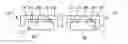
BRIEF DESCRIPTION OF THE DRAWINGSFIGS. 1A-1G illustrate a method according to the first embodiment of the present invention.
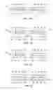
FIGS. 2A-2E illustrate a method according to the second embodiment of the present invention.
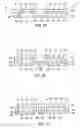
FIG. 3 illustrates an enhanced package that includes a package fabricated in a method according to the second embodiment.
FIG. 4 illustrates an alternative design to the enhanced package shown by FIG. 3.
DETAILED DESCRIPTION OF EMBODIMENTS OF THE INVENTIONReferring to FIG. 1A, in a method of fabrication of a semiconductor package according to the first embodiment of the present invention at least one electrode (not shown specifically), e.g., power electrode of a power semiconductor device such as a power MOSFET, or the emitter electrode of an IGBT, on a front surface 11 of a semiconductor die 10 is electrically and mechanically coupled with a conductive adhesive body 12 (e.g. solder or conductive epoxy) to one portion 14 of a lead frame 16 (formed preferably from copper or a copper alloy). In the preferred embodiment, another electrode (not shown specifically), e.g. control electrode of a power semiconductor device such as the gate electrode of a power MOSFET or IGBT, on a front surface 11 of die 10 is electrically and mechanically coupled to another portion 18 of lead frame 16 with another conductive adhesive body 12 (e.g. solder or conductive epoxy). Note that portion 14 and portion 18 of lead frame 16 are electrically isolated from one another by a gap 20. Further note that in a preferred method a plurality of lead frames 16 are linked together to form a lead frame matrix so that a plurality of semiconductor packages can be fabricated together. Referring next to FIG. 1B, mold compound 22 or a suitable encapsulant is provided to fill the recess in lead frame 16 and to overmold preferably all exposed surfaces of die 10, except for back surface 24 thereof. Next, die 10, mold compound 22 and lead frame 16 are reduced in thickness through, for example, grinding, resulting in the arrangement illustrated by FIG. 1C.
Referring next to FIG. 1D, a seed layer 26 of metallic material, e.g. copper, is formed by sputtering or the like on back surface 24 of die 10. Seed layer 26 preferably extends over portions of mold compound 22 and lead frame portion 14, 18 that are coplanar with back surface 24.
Referring next to FIG. 1E, through a masking and etching process selected portions of seed layer 26 are removed, leaving portions of seed layer 26 over back surface 24 and portions of lead frame 14, 18 that are coplanar with back surface 24 of die 10. Thereafter, through a plating process (e.g. electroless plating or electro plating) a thick metallic body 28 (e.g. copper) is grown over seed layer 26 to obtain a plurality of semiconductor packages as shown by FIG. 1F, and then the semiconductor packages are singulated from the lead frame matrix as illustrated by FIG. 1G to obtain individual semiconductor packages. Note that to render metallic body 28 solderable it can be coated with a solderable finish (e.g. electroless Ni/Au or electroless Ni/Ag) prior to the singulating step.
In a method according to the first embodiment of the present invention lead frame 16 includes a recess which at least partially receives die 10.
Referring next to FIG. 2A, in a method according to the second embodiment of the present invention, a flat copper web 30 (e.g. a thick copper plate) is provided with a passivation body 32 on one surface thereof which has been patterned to receive a plurality of semiconductor die 10. Specifically, an electrode of a die 10 can be electrically and mechanically coupled to web 30 with a conductive adhesive body 12 (e.g. solder or conductive epoxy) through a corresponding opening in passivation 32. Thus, for example, a power electrode of a power semiconductor device such as the source electrode of a power MOSFET, or the emitter electrode of an IGBT, can be coupled to web 30. Similarly, the control electrode of the power semiconductor device, e.g. the gate electrode of the power MOSFET or the IGBT, can be coupled to web 30 through a respective opening in passivation 32.
Referring next to FIG. 2B, mold compound 22 or a suitable encapsulant is applied over die 10, overmolding the exposed surfaces thereof. Next, a portion of die 10 is removed from the back surface 24 thereof through grinding or the like process. Note that naturally some of mold compound 22 will also be removed in the process resulting in the arrangement shown by FIG. 2C.
Thereafter, seed layer 26 (e.g. copper seed layer) is applied to the back surface 24 of die 10, and a metallic body 28 (e.g. copper body) is grown over seed layer 26 as illustrated by FIG. 2D. Next, through a masking and etching process web 30 is patterned whereby the portion thereof coupled to the power electrode is electrically isolated from the portion coupled to the control electrode of die 10. Web 30 is then singulated to obtain a plurality of semiconductor packages as shown by FIG. 2E.
To further enhance each package that is fabricated according to the second embodiment, a conductive clip can be electrically and mechanically coupled to metallic body 28 by a conductive adhesive body (e.g. solder or conductive epoxy).
For example, referring to FIG. 3, a clip 34 having a lead 33 extending outwardly (away from die 10) and a connection surface 36 that is generally coplanar with lead frame portions coupled to the power electrode and the control electrode of die 10 can be coupled to metallic body 28 of a package fabricated according to the present invention. Note that clip 34 may be cup-shaped as shown in U.S. Pat. No. 6,624,522, assigned to the assignee of the present invention.
Referring to FIG. 4, in an alternative design lead 33 may extend inwardly (toward die 10).
The present invention should not be understood to be limited to silicon-based semiconductor devices. Other semiconductor devices such as III-nitride based semiconductor devices can be used without deviating from the scope and spirit of the present invention.
In addition, the present invention is not limited to one semiconductor die per package. Rather, multiple die may be thermally and mechanically coupled to the lead frame in the manner described above before overmolding and other steps are carried out to obtain a package that includes more than one die.
Although the present invention has been described in relation to particular embodiments thereof, many other variations and modifications and other uses will become apparent to those skilled in the art. It is preferred, therefore, that the present invention be limited not by the specific disclosure herein, but only by the appended claims.
Claims
What is claimed is:1. A method of fabricating a semiconductor package, comprising:
electrically and mechanically coupling one electrode on a front surface of a semiconductor die to one portion of a lead frame with a conductive adhesive body;
providing overmolding for said semiconductor die; and
removing a portion of the semiconductor die from the back surface thereof to a desired thickness.
2. The method of claim 1, wherein said lead frame includes a recess in which said semiconductor die is at least partially received.
3. The method of claim 1, further comprising electrically and mechanically coupling another electrode of said semiconductor die to another portion of said lead frame with another conductive adhesive body, said another portion of said lead frame being electrically isolated from said one portion of said lead frame.
4. The method of claim 3, wherein said one electrode is a control electrode and said another electrode is a power electrode of a power semiconductor die.
5. The method of claim 4, wherein said power semiconductor die is one of a power MOSFET and an IGBT.
6. The method of claim 1, further comprising forming a metallic body on said back surface of said semiconductor die.
7. The method of claim 6, wherein said metallic body is formed by growing a seed layer on said back surface of said die following by a plating step.
8. The method of claim 7, wherein said metallic body is comprised of copper.
9. The method of claim 1, further comprising growing a metallic body on said back surface of said semiconductor die and a spaced and electrically isolated metallic body on a lead frame portion coplanar with said back surface of said die.
10. The method of claim 9, wherein said metallic body and said spaced and electrically isolated metallic body are formed by forming a seed layer on said back surface, coplanar portion of said overmolding, and said coplanar portion of said lead frame; etching away selected portion of said seed layer to provide isolation between said seed layer on said back surface and seed layer on said coplanar portion of said lead frame; and plating said seed layer.
11. The method of claim 1, wherein said lead frame is a flat web.
12. The method of claim 1, wherein said lead frame. is a flat web body having a passivation body disposed on one surface thereof; said passivation body including at least one opening therein to receive at least partially said conductive adhesive.
13. The method of claim 12, wherein said passivation body includes at least another opening therein, and further comprising electrically and mechanically coupling another electrode of said power semiconductor die to said lead frame with a conductive adhesive body received at least partially in said another opening.
14. The method of claim 1, further comprising forming a metallic body on said back surface of said semiconductor die.
15. The method of claim 6, wherein said metallic body is formed by growing a seed layer on said back surface of said die followed by a plating step.
16. The method of claim 7, wherein said metallic body is comprised of copper.
17. The method of claim 14, further comprising electrically and mechanically coupling said metallic body to a conductive clip with a conductive adhesive.
18. The method of claim 17, wherein said clip includes a lead portion having a connection surface that is coplanar with lead frame.
19. The method of claim 18, wherein said clip is cup-shaped.
20. The method of claim 18, wherein said lead portion is bent inwardly toward said die.
21. The method of claim 18, wherein said lead portion is ben outwardly away from said die.
22. The method of claim 1, further comprising rendering said metallic body solderable with a solderable finish.
23. The method of claim 22, wherein said solderable finish is comprised of Ni/Au.
24. The method of claim 22, wherein said solderable finish is comprised of Ni/Ag.
25. The method of claim 1, wherein said semiconductor die is a III-nitride semiconductor device.
26. The method of claim 1, further comprising electrically and mechanically coupling one electrode of another die to said one portion of said lead frame.
Images & Drawings included:
Sources:
- United States Patent and Trademark Office - verify current appl. status at the USPTO↗
Similar patent applications:
- » 20210202414
Package substrate including segment grooves arranged in a radial direction of a redistribution pad and semiconductor package including the same - » 20070108585
Semiconductor package including a semiconductor die having redistributed pads - » 20170148692
Semiconductor package including a semiconductor die having redistributed pads - » 20180366380
SEMICONDUCTOR PACKAGE INCLUDING A SEMICONDUCTOR DIE HAVING REDISTRIBUTED PADS - » 20250167153
METHOD OF FORMING REDISTRIBUTION PAD AND METHOD OF MANUFACTURING SEMICONDUCTOR PACKAGE - » 20220238469
Package substrate including a redistribution pad extending from a redistribution layer and including segmenting grooves along a redial direction thereof and semiconductor package including the same
Recent applications in this class:
- » 20250279393 2025-09-04
SEMICONDUCTOR DEVICE PRODUCTION METHOD AND STRUCTURE - » 20250273625 2025-08-28
LOGIC DRIVE BASED ON MULTICHIP PACKAGE USING INTERCONNECTION BRIDGE - » 20250266393 2025-08-21
METHOD FOR FABRICATING ELECTRONIC PACKAGE - » 20250253288 2025-08-07
Semiconductor Device and Method of Forming the Same - » 20250246579 2025-07-31
INTEGRATED CIRCUIT (IC) DEVICE PACKAGING SYSTEM AND METHOD - » 20250233108 2025-07-17
PLURALITY OF ADVANCED MULTILEVEL CIRCUIT ATTACHMENTS - » 20250210586 2025-06-26
SEMICONDUCTOR PACKAGE SUBSTRATE DICING AND EDGE PASSIVATION - » 20250167172 2025-05-22
MICRODEVICE TRANSFER SETUP AND INTEGRATION OF MICRO-DEVICES INTO SYSTEM SUBSTRATE - » 20250167171 2025-05-22
MICRODEVICE TRANSFER SETUP AND INTEGRATION OF MICRO-DEVICES INTO SYSTEM SUBSTRATE - » 20250054905 2025-02-13
SEMICONDUCTOR DEVICE, CHIP AND FABRICATION METHOD THEREOF, MEMORY SYSTEM
Recent applications for this Assignee:
- » 20150130036 2015-05-14
Semiconductor package with low profile switch node integrated heat spreader - » 20150037965 2015-02-05
Fabrication of III-nitride semiconductor device and related structures - » 20150008572 2015-01-08
Power semiconductor package with multiple dies - » 20150001599 2015-01-01
Power semiconductor package with non-contiguous, multi-section conductive carrier - » 20140353680 2014-12-04
Gallium nitride semiconductor structures with compositionally-graded transition layer - » 20140339686 2014-11-20
Group III-V device with a selectively modified impurity concentration - » 20140339651 2014-11-20
Semiconductor device with a field plate double trench having a thick bottom dielectric - » 20140332879 2014-11-13
Power semiconductor device with reduced on-resistance and increased breakdown voltage - » 20140327014 2014-11-06
III-nitride rectifier package - » 20140319665 2014-10-30
Power semiconductor package