Power semiconductor module
US20070102796A1
2007-05-10
11/595,082
2006-11-09
✅ Patent granted
US 7,638,872 B2
2009-12-29
-
-
Thao X Le | Thanh Y Tran
2027-05-16
Abstract:
A power semiconductor module is presented. The power semiconductor module has a substrate, a composite film, and a power semiconductor component between the substrate and the composite film. The composite film has a thin circuit-structured logic metal layer and a thick circuit-structured power metal layer and between them a thin electrically insulating plastic film. The composite film includes contact nubs, which provide bonding to the power semiconductor component. Feedthrough holes are provided between the logic metal layer and the power metal layer. The plastic film in the region of the respective through-plated hole includes a recess in a region that is free of the logic metal layer. A segment of a flexible thin wire extends through the free region of the logic metal layer and through the recess in the plastic film and is bonded to the logic metal layer and the power metal layer by means of bonding sites.
Inventors:
- Christian Goebl 3 🇩🇪 Nuernberg, Germany
- Karlheinz Augustin 2 🇩🇪 Fuerth, Germany
- Christian Goebl 2 🇩🇪 Nuremberg, Germany
Assignee:
- Semikron Elektronik GmbH & Co., KG 78 🇩🇪 Nürnberg, Germany
Interested in similar patents?
Get notified when new applications in this technology area are published.
Classification:
H01L23/48 IPC
Details of semiconductor or other solid state devices Arrangements for conducting electric current to or from the solid state body in operation, e.g. leads, terminal arrangements ; Selection of materials therefor
H05K3/4007 » CPC main
Apparatus or processes for manufacturing printed circuits; Forming printed elements for providing electric connections to or between printed circuits Surface contacts, e.g. bumps
H05K3/4007 » CPC main
Apparatus or processes for manufacturing printed circuits; Forming printed elements for providing electric connections to or between printed circuits Surface contacts, e.g. bumps
H01L23/4985 » CPC further
Details of semiconductor or other solid state devices; Arrangements for conducting electric current to or from the solid state body in operation, e.g. leads, terminal arrangements ; Selection of materials therefor consisting of soldered constructions; Leads, on insulating substrates, Flexible insulating substrates
H01L23/5389 » CPC further
Details of semiconductor or other solid state devices; Arrangements for conducting electric current within the device in operation from one component to another, i.e. interconnections, e.g. wires, lead frames the interconnection structure between a plurality of semiconductor chips being formed on, or in, insulating substrates the chips being integrally enclosed by the interconnect and support structures
H01L24/24 » CPC further
Arrangements for connecting or disconnecting semiconductor or solid-state bodies; Methods or apparatus related thereto; Means for bonding being attached to, or being formed on, the surface to be connected, e.g. chip-to-package, die-attach, "first-level" interconnects; Manufacturing methods related thereto; High density interconnect [HDI] connectors; Manufacturing methods related thereto; Structure, shape, material or disposition of the high density interconnect connectors after the connecting process of an individual high density interconnect connector
H01L24/48 » CPC further
Arrangements for connecting or disconnecting semiconductor or solid-state bodies; Methods or apparatus related thereto; Means for bonding being attached to, or being formed on, the surface to be connected, e.g. chip-to-package, die-attach, "first-level" interconnects; Manufacturing methods related thereto; Wire connectors; Manufacturing methods related thereto; Structure, shape, material or disposition of the wire connectors after the connecting process of an individual wire connector
H01L25/072 » CPC further
Assemblies consisting of a plurality of individual semiconductor or other solid state devices ; Multistep manufacturing processes thereof all the devices being of a type provided for in the same subgroup of groups - , e.g. assemblies of rectifier diodes the devices not having separate containers the devices being of a type provided for in group the devices being arranged next to each other
H05K1/0265 » CPC further
Printed circuits; Details; Electrical arrangements not otherwise provided for; High current adaptations, e.g. printed high current conductors or using auxiliary non-printed means; Fine and coarse circuit patterns on one circuit board characterized by the lay-out of or details of the printed conductors, e.g. reinforced conductors, redundant conductors, conductors having different cross-sections
H05K3/4046 » CPC further
Apparatus or processes for manufacturing printed circuits; Forming printed elements for providing electric connections to or between printed circuits; Through-connections; Vertical interconnect access [VIA] connections using auxiliary conductive elements, e.g. metallic spheres, eyelets, pieces of wire
H01L23/49833 » CPC further
Details of semiconductor or other solid state devices; Arrangements for conducting electric current to or from the solid state body in operation, e.g. leads, terminal arrangements ; Selection of materials therefor consisting of soldered constructions; Leads, on insulating substrates, the chip support structure consisting of a plurality of insulating substrates
H01L23/5385 » CPC further
Details of semiconductor or other solid state devices; Arrangements for conducting electric current within the device in operation from one component to another, i.e. interconnections, e.g. wires, lead frames the interconnection structure between a plurality of semiconductor chips being formed on, or in, insulating substrates Assembly of a plurality of insulating substrates
H01L23/5387 » CPC further
Details of semiconductor or other solid state devices; Arrangements for conducting electric current within the device in operation from one component to another, i.e. interconnections, e.g. wires, lead frames the interconnection structure between a plurality of semiconductor chips being formed on, or in, insulating substrates Flexible insulating substrates
H01L24/45 » CPC further
Arrangements for connecting or disconnecting semiconductor or solid-state bodies; Methods or apparatus related thereto; Means for bonding being attached to, or being formed on, the surface to be connected, e.g. chip-to-package, die-attach, "first-level" interconnects; Manufacturing methods related thereto; Wire connectors; Manufacturing methods related thereto; Structure, shape, material or disposition of the wire connectors prior to the connecting process of an individual wire connector
H01L24/50 » CPC further
Arrangements for connecting or disconnecting semiconductor or solid-state bodies; Methods or apparatus related thereto; Means for bonding being attached to, or being formed on, the surface to be connected, e.g. chip-to-package, die-attach, "first-level" interconnects; Manufacturing methods related thereto Tape automated bonding [TAB] connectors, i.e. film carriers; Manufacturing methods related thereto
H01L2224/2518 » CPC further
Indexing scheme for arrangements for connecting or disconnecting semiconductor or solid-state bodies and methods related thereto as covered by; Means for bonding being attached to, or being formed on, the surface to be connected, e.g. chip-to-package, die-attach, "first-level" interconnects; Manufacturing methods related thereto; High density interconnect [HDI] connectors; Manufacturing methods related thereto; Structure, shape, material or disposition of the high density interconnect connectors after the connecting process of a plurality of high density interconnect connectors; Disposition being disposed on at least two different sides of the body, e.g. dual array
H01L2924/01006 » CPC further
Indexing scheme for arrangements or methods for connecting or disconnecting semiconductor or solid-state bodies as covered by; Chemical elements Carbon [C]
H01L2924/01013 » CPC further
Indexing scheme for arrangements or methods for connecting or disconnecting semiconductor or solid-state bodies as covered by; Chemical elements Aluminum [Al]
H01L2924/01027 » CPC further
Indexing scheme for arrangements or methods for connecting or disconnecting semiconductor or solid-state bodies as covered by; Chemical elements Cobalt [Co]
H01L2924/01029 » CPC further
Indexing scheme for arrangements or methods for connecting or disconnecting semiconductor or solid-state bodies as covered by; Chemical elements Copper [Cu]
H01L2924/01033 » CPC further
Indexing scheme for arrangements or methods for connecting or disconnecting semiconductor or solid-state bodies as covered by; Chemical elements Arsenic [As]
H01L2924/01068 » CPC further
Indexing scheme for arrangements or methods for connecting or disconnecting semiconductor or solid-state bodies as covered by; Chemical elements Erbium [Er]
H01L2924/01082 » CPC further
Indexing scheme for arrangements or methods for connecting or disconnecting semiconductor or solid-state bodies as covered by; Chemical elements Lead [Pb]
H01L2924/19107 » CPC further
Indexing scheme for arrangements or methods for connecting or disconnecting semiconductor or solid-state bodies as covered by; Details of hybrid assemblies other than the semiconductor or other solid state devices to be connected; Disposition of discrete passive components off-chip wires
H05K1/0393 » CPC further
Printed circuits; Details; Use of materials for the substrate Flexible materials
H05K1/0393 » CPC further
Printed circuits; Details; Use of materials for the substrate Flexible materials
H05K1/09 » CPC further
Printed circuits; Details Use of materials for the conductive, e.g. metallic pattern
H05K1/09 » CPC further
Printed circuits; Details Use of materials for the conductive, e.g. metallic pattern
H05K2201/0352 » CPC further
Indexing scheme relating to printed circuits covered by; Conductive materials; Structure of the conductor; Layered conductors or foils Differences between the conductors of different layers of a multilayer
H05K2201/0352 » CPC further
Indexing scheme relating to printed circuits covered by; Conductive materials; Structure of the conductor; Layered conductors or foils Differences between the conductors of different layers of a multilayer
H05K2201/0367 » CPC further
Indexing scheme relating to printed circuits covered by; Conductive materials; Structure of the conductor; Conductor shape Metallic bump or raised conductor not used as solder bump
H05K2201/0367 » CPC further
Indexing scheme relating to printed circuits covered by; Conductive materials; Structure of the conductor; Conductor shape Metallic bump or raised conductor not used as solder bump
H05K2201/09736 » CPC further
Indexing scheme relating to printed circuits covered by; Shape and layout; Shape and layout details of conductors covering at least two types of conductors provided for in - Varying thickness of a single conductor; Conductors in the same plane having different thicknesses
H05K2201/10166 » CPC further
Indexing scheme relating to printed circuits covered by; Details of components or other objects attached to or integrated in a printed circuit board; Types of components Transistor
H05K2201/10166 » CPC further
Indexing scheme relating to printed circuits covered by; Details of components or other objects attached to or integrated in a printed circuit board; Types of components Transistor
H05K2203/049 » CPC further
Indexing scheme relating to apparatus or processes for manufacturing printed circuits covered by; Soldering or other types of metallurgic bonding Wire bonding
H05K2203/049 » CPC further
Indexing scheme relating to apparatus or processes for manufacturing printed circuits covered by; Soldering or other types of metallurgic bonding Wire bonding
H01L2924/00 » CPC further
Indexing scheme for arrangements or methods for connecting or disconnecting semiconductor or solid-state bodies as covered by
H01L2924/00014 » CPC further
Indexing scheme for arrangements or methods for connecting or disconnecting semiconductor or solid-state bodies as covered by; Technical content checked by a classifier the subject-matter covered by the group, the symbol of which is combined with the symbol of this group, being disclosed without further technical details
H01L2924/20757 » CPC further
Indexing scheme for arrangements or methods for connecting or disconnecting semiconductor or solid-state bodies as covered by; Parameters; Diameter ranges larger or equal to 70 microns less than 80 microns
H01L23/02 IPC
Details of semiconductor or other solid state devices Containers; Seals
H01L23/34 IPC
Details of semiconductor or other solid state devices Arrangements for cooling, heating, ventilating or temperature compensation ; Temperature sensing arrangements
Description
BACKGROUND OF THE INVENTION1. Field of the Invention
The invention relates to a power semiconductor module, having a substrate, a composite film, and at least one power semiconductor component between the substrate and the composite film, which power semiconductor component has a thin circuit-structured logic metal layer and compared to it a thick circuit-structured power metal layer and between them a thin electrically insulating plastic film, the composite film being embodied with contact nubs for bonding to the at least one power semiconductor component, and through-plated holes are provided between the logic metal layer and the power metal layer.
2. Description of the Related Art
One such power semiconductor module is known from German Patent Disclosure DE 103 55 925 A1 filed by the present Applicant. In this known power semiconductor module, the through-plated holes are produced for instance by laser drilling and ensuing laser-supported filling with a conductive material. Through-plated holes with a diameter of a few hundred micrometers are thus possible. The production of such through-plated holes involves not insignificant effort and expense. Moreover, in the process of filling with conductive material, care must be taken that the filling material be adapted in its material properties, such as its coefficient of thermal expansion, to the materials of the composite film.
SUMMARY OF THE INVENTIONGiven these known conditions, it is an object of the invention to create a power semiconductor module of the type defined at the outset, which can be produced simply and economically, and in which the through-plated holes can be produced simply and reliably.
The object is met by a power semiconductor module having a substrate, a composite film, and at least one power semiconductor component between the substrate and the composite film, the composite film having a thin circuit-structured logic metal layer, a comparatively thick circuit-structured power metal layer, and between them a thin electrically insulating plastic film, the composite film being embodied with contact nubs for bonding to the at least one power semiconductor component, and feedthrough holes or through-plated holes are provided between the logic metal layer and the power metal layer, wherein in a region of each through-plated hole, the plastic film is embodied with a recess in a region that is free of the logic metal layer and that a flexible segment of a thin wire extends through the region that is free of the logic metal layer and through the recess in the plastic film and is bonded to the logic metal layer and to the power metal layer by bonding.
In the power semiconductor module of the invention, it is preferred if the circuit structures of the logic metal layer and the circuit structures of the power metal layer are produced in a single operation, that is, simultaneously by etching. This etching operation is performed in a manner known per se. This expediently involves mask etching of the composite film, which can advantageously be done quasi-endlessly continuously.
The logic metal layer of the semiconductor module of the invention is preferably a copper layer, and its power metal layer is preferably an aluminum layer. The plastic film between the logic metal layer and the power metal layer preferably comprises polyimide.
In the composite film of the semiconductor module of the invention, the logic metal layer and the power metal layer are preferably two-dimensionally glued to the plastic film.
Each recess in the plastic film of the composite film of the power semiconductor module of the invention is preferably produced by lasing. For that purpose, a CO2 inscription laser may, for example, be employed.
The thin wire of each through-plated hole preferably comprises aluminum having, for example, a diameter of 25-100 μm. The bonded connection of the thin wire to the thin circuit-structured logic metal layer and to the thicker circuit-structured power metal layer is expediently done with a standard thin-wire bonder.
The power semiconductor module of the invention has the advantage that each through-plated hole is very flexible and reliable. The thin wire for connecting the logic metal layer and the power metal layer has a flexibility which takes the flexibility of the logic metal layer and the power metal layer into account.
After the bonding of the thin wire to the logic metal layer and the power metal layer, each through-plated hole can be stamped and covered with a suitable insulating material as needed.
Further details, characteristics, and advantages will become apparent from the ensuing description of an exemplary embodiment of the power semiconductor module of the invention, which is shown schematically in the drawing and not to scale.
Other objects and features of the present invention will become apparent from the following detailed description considered in conjunction with the accompanying drawings. It is to be understood, however, that the drawings are designed solely for purposes of illustration and not as a definition of the limits of the invention, for which reference should be made to the appended claims. It should be further understood that the drawings are not necessarily drawn to scale and that, unless otherwise indicated, they are merely intended to conceptually illustrate the structures and procedures described herein.
BRIEF DESCRIPTION OF THE DRAWINGSIn the drawings:
FIG. 1, in an enlarged sectional view, not to scale, showing portions of an embodiment of the power semiconductor module; and
FIG. 2 shows a further-enlarged sectional view of the detail marked 11 in FIG. 1.
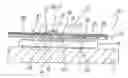
DETAILED DESCRIPTION OF THE PRESENTLY PREFERRED EMBODIMENTSFIG. 1 shows some portions in section of an embodiment of the power semiconductor module 10 having a substrate 12, a composite film 14, and a power semiconductor component 16 that is provided between the substrate 12 and the composite film 14. The power semiconductor component 16 has a collector 18, an emitter 20, and a gate 22.
The composite film has a thin electrically insulating plastic film 24 provided on a first main face with a thin circuit-structured logic metal layer 26 and on a second main face opposing the first main face with a circuit-structured power metal layer 28.
The composite film 14 is embodied with nubs 30, which serve the purpose of bonding to the power semiconductor component 16.
Between the thin circuit-structured logic metal layer 26 and the circuit-structured power metal layer 28, feedthrough holes or through-plated holes 32 are provided, of which in FIG. 1 only one through-plated hole 32 is shown. As can be seen clearly from FIG. 2, the electrically insulating plastic film 24 is embodied with a recess 34 in the region of each through-plated hole 32. The recess 34 is embodied in the region 36 that because of its structuring is free of the logic metal layer 26, or in other words under this region.
A flexible segment 38 of a thin wire 40 is firmly bonded by its end portion 42 to the circuit-structured logic metal layer 26. This is indicated by reference numeral 44. The second end portion 46, remote from it, of the thin wire 40 is firmly bonded to the circuit-structured power metal layer 28. This bonding site is identified by reference numeral 48.
In FIGS. 1 and 2, identical details are identified by the same reference numerals, so there is no need to describe all the details again in conjunction with FIGS. 1 and 2.
Thus, while there have shown and described and pointed out fundamental novel features of the invention as applied to a preferred embodiment thereof, it will be understood that various omissions and substitutions and changes in the form and details of the devices illustrated, and in their operation, may be made by those skilled in the art without departing from the spirit of the invention. For example, it is expressly intended that all combinations of those elements and/or method steps, which perform substantially the same function in substantially the same way to achieve the same results, are within the scope of the invention. Moreover, it should be recognized that structures and/or elements and/or method steps shown and/or described in connection with any disclosed form or embodiment of the invention may be incorporated in any other disclosed or described or suggested form or embodiment as a general matter of design choice. It is the intention, therefore, to be limited only as indicated by the scope of the claims appended hereto.
Claims
1. A power semiconductor module, comprising:
a substrate;
at least one power semiconductor component on the substrate; and
a composite film arranged on the at least one power semiconductor component such that the at least on one power semiconductor component is between the substrate and the composite film,
wherein the composite film has a thin circuit-structured logic metal layer, a comparatively thick circuit-structured power metal layer, and a thin electrically insulating film disposed between the circuit-structured logic metal layer and the circuit-structured power metal layer, the composite film having contact nubs for bonding to the at least one power semiconductor component,
wherein feedthrough holes are provided between the logic metal layer and the power metal layer, the plastic film defining a recess in the region of each feedthrough hole that is free of the logic metal layer, and
wherein a flexible segment of a thin wire extends through the region that is free of the logic metal layer and through the recess in the plastic film and is bonded to bonding sites at each of the logic metal layer and the power metal layer.
2. The power semiconductor module of claim 1, wherein the circuit structures of the logic metal layer and of the power metal layer are produced simultaneously by etching.
3. The power semiconductor module of claim 1, wherein the logic metal layer is a copper layer and the power metal layer is an aluminum layer.
4. The power semiconductor module of claim 1, wherein the plastic film comprises polyimide.
5. The power semiconductor module of claim 1, wherein the logic metal layer and the power metal layer are adhered two-dimensionally to the plastic film.
6. The power semiconductor module of claim 1, wherein each recess in the plastic film is produced by lasing.
7. The power semiconductor module of claim 1, wherein the thin wire comprises aluminum.
8. The power semiconductor module of claim 1, wherein the thin wire has a diameter of 25-100 μm.
9. The power semiconductor module according to claim 1, wherein the feedthrough hole is covered with an insulating material.
Images & Drawings included:
Sources:
- United States Patent and Trademark Office - verify current appl. status at the USPTO↗
Similar patent applications:
- » 20220139797
Semiconductor module, power semiconductor module, and power electronic equipment using the semiconductor module or the power semiconductor module - » 20100252922
Power semiconductor module, power semiconductor module assembly and method for fabricating a power semiconductor module assembly - » 20240260168
CIRCUIT BOARD FOR A POWER SEMICONDUCTOR MODULE, POWER SEMICONDUCTOR MODULE, AND METHOD FOR PRODUCING A CIRCUIT BOARD AND A POWER SEMICONDUCTOR MODULE - » 20230155479
Power semiconductor module, power electronic assembly including one or more power semiconductor modules, and power conversion control circuit for a power semiconductor module - » 20140225245
Power semiconductor module and power semiconductor module assembly with multiple power semiconductor modules - » 20250259909
A HEAT DISSIPATION SUBSTRATE FOR A POWER SEMICONDUCTOR MODULE, A POWER SEMICONDUCTOR MODULE INCLUDING THE SAME AND A POWER CONVERTER INCLUDING THE SAME, AND MANUFACTURING METHOD OF THE HEAT DISSIPATION SUBSTRATE FOR A POWER SEMICONDUCTOR MODULE - » 20250259908
HEAT DISSIPATION SUBSTRATE FOR A POWER SEMICONDUCTOR MODULE, A POWER SEMICONDUCTOR MODULE INCLUDING THE SAME AND A POWER CONVERTER INCLUDING THE SAME, AND MANUFACTURING METHOD OF THE HEAT DISSIPATION SUBSTRATE FOR A POWER SEMICONDUCTOR MODULE - » 20250118636
HEAT DISSIPATION SUBSTRATE FOR A POWER SEMICONDUCTOR MODULE, A POWER SEMICONDUCTOR MODULE INCLUDING THE HEAT DISSIPATION SUBSTRATE, AND A POWER CONVERTER INCLUDING THE POWER SEMICONDUCTOR MODULE - » 20250118680
HEAT DISSIPATION SUBSTRATE FOR A POWER SEMICONDUCTOR MODULE, A POWER SEMICONDUCTOR MODULE INCLUDING THE HEAT DISSIPATION SUBSTRATE, AND A POWER CONVERTER INCLUDING THE POWER SEMICONDUCTOR MODULE - » 20230170287
POWER SEMICONDUCTOR MODULE, METHOD FOR ASSEMBLING A POWER SEMICONDUCTOR MODULE AND HOUSING FOR A POWER SEMICONDUCTOR MODULE
Recent applications in this class:
- » 20250185180 2025-06-05
PRINTED CIRCUIT BOARD AND MANUFACTURING METHOD THEREOF - » 20250126722 2025-04-17
CIRCUIT COMPENSATION METHOD APPLIED TO PATTERN DISPLACEMENT AND CIRCUIT STRUCTURE - » 20250107008 2025-03-27
PRINTED CIRCUIT BOARD - » 20250098076 2025-03-20
BOARD AND ELECTRONIC DEVICE - » 20240188224 2024-06-06
Electrical devices with electrodes on softening polymers and methods of manufacturing thereof - » 20240164026 2024-05-16
PRINTED CIRCUIT BOARD - » 20240107683 2024-03-28
WIRING CIRCUIT BOARD - » 20230180396 2023-06-08
Electrical devices with electrodes on softening polymers and methods of manufacturing thereof - » 20230007787 2023-01-05
Flux dotting tool - » 20220377910 2022-11-24
PREPARATION METHOD FOR CONNECTOR ELECTRONIC DEVICE CONNECTOR AND APPLICATION THEREOF
Recent applications for this Assignee:
- » 20170186673 2017-06-29
Power semiconductor arrangement - » 20170176501 2017-06-22
Centering holding device for a Rogowski coil and a method for arranging a Rogowski coil - » 20170148710 2017-05-25
Power electronic switching device comprising a plurality of potential surfaces - » 20170144246 2017-05-25
Apparatus for the material-bonded connection of connection partners of a power-electronics component - » 20170062296 2017-03-02
Power electronic submodule comprising a bipartite housing - » 20170025806 2017-01-26
Arrangement having a power-electronic component and a DC-voltage busbar - » 20170005594 2017-01-05
Power semiconductor circuit having a field effect transistor with low energy losses - » 20160234926 2016-08-11
Arrangement with a power semiconductor module, having a DC-voltage busbar and a capacitor - » 20160120038 2016-04-28
Method for producing a switching device with a moisture-tight and electrically insulating cover and for producing an arrangement therewith - » 20150325494 2015-11-12
Power semiconductor module with switching device and assembly